Wide-field microwave magnetic field imaging with nitrogen-vacancy centers in diamond
Abstract
Non-invasive imaging of microwave (MW) magnetic fields with microscale lateral resolution is pivotal for various applications, such as MW technologies and integrated circuit failure analysis. Diamond nitrogen-vacancy (NV) center magnetometry has emerged as an ideal tool, offering m-scale resolution, millimeter-scale field of view, high sensitivity, and non-invasive imaging compatible with diverse samples. However, up until now, it has been predominantly used for imaging of static or low-frequency magnetic fields or, concerning MW field imaging, to directly characterize the same microwave device used to drive the NV spin transitions. In this work we leverage an NV center ensemble in diamond for wide-field imaging of MW magnetic fields generated by a test device employing a differential measurement protocol. The microscope is equipped with a MW loop to induce Rabi oscillations between NV spin states, and the MW field from the device-under-test is measured through local deviations in the Rabi frequency. This differential protocol yields magnetic field maps of a 2.57 GHz MW field with a sensitivity of 9 T Hz-1/2 for a total measurement duration of s, covering a m2 field of view with a m-scale spatial resolution and a DUT input power dynamic range of 30 dB. This work demonstrates a novel NV magnetometry protocol, based on differential Rabi frequency measurement, that extends NV wide-field imaging capabilities to imaging of weak MW magnetic fields that would be difficult to measure directly through standard NV Rabi magnetometry.
I Introduction
The detection and imaging of microwave (MW) magnetic fields is of significant importance for a variety of applications, from probing magnetic excitations such as spin waves[1] and spin liquids is frustrated magnets[2], to mapping the AC susceptibility of magnetic materials[3], as well as imaging of biological samples[4]. Of particular interest is the use of MW imaging for MW devices characterization[5, 6], as such devices represent the building blocks of many critical technologies[7, 8], including quantum information processing[9, 10, 11, 12]. For this reason, a reliable technique that gives insight on the device functioning with localized information on the device internal features - something that the usual external-port measurements cannot do[13] - by imaging the spatial distribution of MW fields with microscale resolution over a wide filed of view is critical for the development of the aforementioned MW technologies.
Nitrogen-vacancy (NV) centers in diamond have emerged as a promising tool for imaging magnetic fields [14] over a wide range of samples and for both static and dynamic fields [15] due to their magnetically-sensitive fluorescence emitted upon optical excitation[16, 17]. Indeed, magnetometry based on NV centers in diamond has already been employed to image static magnetic fields from current flow in 2D materials [18, 19], to observe ferromagnetic domains for magnetic memory [20] and hardware security [21] applications, for characterization of integrated circuits [22, 23], as well as to characterize biological samples [24, 25]. Imaging of MW fields has already been demonstrated, with both NV ensembles[26, 27] and single-NV scanning probes[28], by measuring Rabi oscillations induced by the MW field within NV spin sublevels. The main limitation in these previous works is that the microwave device under test also serves as the antenna driving the NV spin transitions, which restricts the range of devices and signal strengths that can be observed. To overcome this limitation, we develop a novel method that enables to measure weak MW signals that cannot be directly measured, using a differential Rabi measurement technique.
In this work, we demonstrate wide-field imaging of MW magnetic fields in the GHz range from a device-under-test (DUT) by detecting small deviations of the NV spin sublevels Rabi oscillations around a central Rabi frequency through a differential measurement protocol. In this experiment, Rabi oscillations are driven by a MW loop operating at high power (40 dBm), positioned near the NV layer, while the DUT is deliberately operated at much lower power (in the range -2 to 28 dBm) to generate weak MW fields. We observe that, although the MW field from the DUT is too weak to directly drive Rabi oscillations, it can still be measured using a differential Rabi measurements. By employing a three-stage pulse sequence, alternating between driving Rabi oscillations with the MW loop alone and with both the MW loop and DUT, we can observe how the Rabi oscillations driven by the MW loop are altered when the DUT is active. This differential technique allows to extend the detectable MW power range by an additional 40 dB of DUT MW input power. The NV photoluminescence (PL) is collected with a CMOS camera, offering spatially-resolved details on the local variations in the Rabi frequency across the field of view, thus giving information on the MW field generated by the DUT. As a proof-of-principle experiment, the DUT is a fabricated 100 m-wide 200 nm-thick Cu stripline. After describing the experimental setup and the measurement protocol, we demonstrate the MW imaging capability of magnetic fields oscillating at 2.57 GHz over a field of view of m2. Moreover, we demonstrate MW imaging capabilities over dynamic range of 30 dB in the DUT input power with a measured magnetic field sensitivity of 9 T Hz-1/2 over a single pixel with size of m2. In addition, to demonstrate the versatility of the Rabi differential method here developed, we image a different nontrivial DUT. This work establishes a novel procedure to use NV quantum sensing to perform wide-field imaging of high-frequency magnetic fields. The described protocol allows us to measure weak signals, thus expanding the range of samples that can be studied by NV magnetometry, with potential applications across diverse fields, from life sciences to MW device failure analysis.
II Experimental methods
II.1 Experimental setup
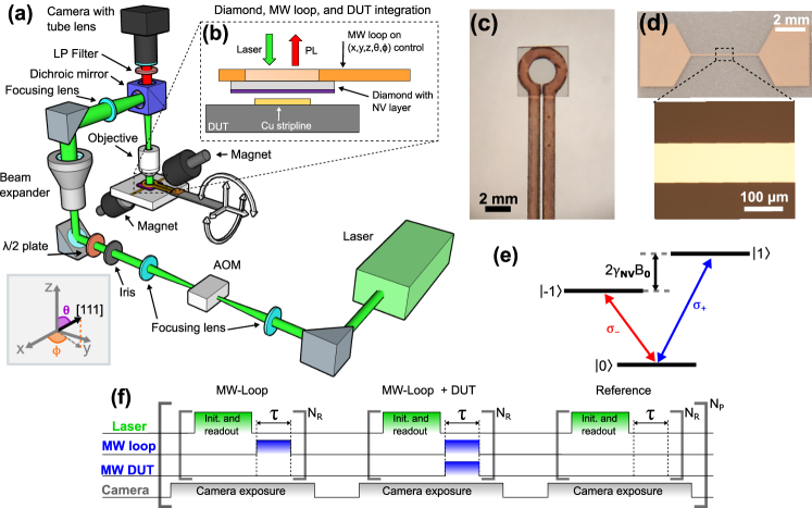
The schematics of the home-built fluorescence microscope we use to perform wide-field MW magnetic field imaging is shown in Fig. 1(a). A 532 nm laser is pulsed with an AOM before being appropriately focused on the back aperture of a 20 0.4 NA objective, to achieve a uniform illumination on a FOV of m2. The PL emitted by the NVs is then collected by a CMOS camera after being filtered with a 650 nm long-pass filter. Before analysis we apply 4x4 pixel binning, resulting in a m2 pixel size. However, the lateral resolution in this experiment is likely limited by the NV layer thickness and the diamond-DUT stand-off distance. Two permanent magnets mounted on motorized translation stages for angle and radial control are used to apply a bias magnetic field aligned to the [111] crystallographic NV axis; the orientation with respect to the laboratory reference frame (, ) is also shown in the inset of Fig. 1(a). The diamond sensor, consisting of a 4 m-thick NV layer overgrown on a 500 m-thick diamond plate, is glued on the MW loop (operated at a power of 40 dBm) that is used to drive the spin transitions. The diamond/MW loop system is in turn mounted on a 5 axis () translation stage, that we use to bring the diamond in proximity of the DUT, as shown in Fig. 1(b). An optical picture showing the MW loop with the diamond glued on it is reported in Fig. 1(c), whereas Fig. 1(d) shows an optical picture of the DUT, consisting of a 100 m wide, 200 nm thick Cu stripline deposited on a Al2O3 substrate. More details on the experimental setup are reported in the SI[29].
II.2 Detection mechanism
The negatively-charged NV electronic ground state is a spin system, with the sublevels separated from the doubly-degenerate sublevels by the zero-field splitting GHz. Through the Zeeman effect, the bias magnetic field removes the degeneracy of the states by a factor , where kHz T-1 is the NV gyromagnetic ratio. This allows us to use either or as an isolated two-level system, as shown in Fig. 1(e). Due to selection rules, the two separate transitions () are only excited by a circularly polarized MW fields[28]. Thus, the two transitions are only sensitive to a single polarization component , with and being respectively the left- and right-handed circularly polarized component of the MW field, with the polarization axis parallel to the NV axis. A MW field resonant with either transition will then result in population oscillations between the relevant spin sublevels, i.e. Rabi oscillations, at a frequency of . In the following, we only use for demonstration of MW magnetic field imaging. In particular we use a bias field mT leading to a resonant frequency GHz (measured with optically detected magnetic resonance spectrum). We emphasize that , the frequency of the MW field we are sensitive to, can be changed simply by adjusting . For simplicity in the notation, for the remaining of this manuscript we will suppress the “-” subscript as, unless otherwise stated, we are referring to only the transition.
II.3 Pulse sequence
We drive both the MW loop and the DUT with a MW current having same frequency GHz and measure the Rabi oscillations with the pulse sequence reported in Fig. 1(f), extended from Horsley et al [26]. The sequence is divided in three sections: the first “MW-loop” where a MW pulse is only supplied to the MW loop line; the second “MW-loop + DUT” where two MW pulses of same duration are sent in both MW loop and DUT; and the third “reference” where the bare fluorescence of the state is measured without applying any MW pulse. For each section, the sequence starts with a laser pulse (15 s duration) that both initializes the NVs into the state and reads out their spin state. The laser pulse is followed by the MW pulse (or pulses) of duration that drives the Rabi oscillation. This sequence is repeated times inside a single camera exposure time (6 ms) to accumulate PL counts. For each value of , a total of images are collected per each section and then averaged to further increase the signal to noise ratio. This whole sequence is repeated as we scan the MW pulse duration in the interval [0,1.2 s] to measure the Rabi oscillations. Keeping the camera open during several repetitions of the laser and MW pulse sequence leads to a decrease in the contrast, as the spin readout and the NV center repolarization to the state occur simultaneously [30]. However, this allows us to accumulate more experiment repetitions and to gate the camera at a timescale much longer than the characteristic Rabi oscillation time. At the end of the sequence we obtain three separate PL vs. time measurements for the three MW pulse combinations described above. The “reference” measurement is subtracted to the other two measurements to remove the background fluorescence and correct any possible non-uniformity in the background. We then obtain two sets of measurements that we refer to respectively and .
III Results and Discussion
III.1 MW magnetic field imaging
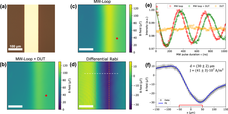
Using the pulse sequence from Fig. 1(f), we obtain a series of images where each pixel contains a Rabi oscillation that we fit with the equation:
| (1) |
with being the MW pulse length while the fitting parameters are fluorescence intensity , Rabi fluorescence contrast , Rabi decay lifetime , and Rabi frequency . We can then assign to each pixel the corresponding value of magnetic field through the relation . The results for the wide-field measurement obtained for a MW power in the DUT of 17.8 dBm are shown in Fig. 2(b) and (c) for and . Figure 2(e) shows a typical example of Rabi oscillations for (green curve) and (red curve) for a single pixel (red star in Fig. 2(b) and (c)). We notice that the MW field generated by the DUT is not strong enough to be detected directly. This can be observed from the yellow curve in Fig. 2(e), showing a single-pixel scan measured when the MW pulse is sent only in the DUT (not shown in Fig. 1(f)), where no Rabi oscillations can be observed. Measuring alone does not carry useful information, as it cannot be fit through Eq. 1. To isolate the contribution of the DUT from the total magnetic field we use the following equation
| (2) |
where we assumed that and the factor results from the root mean square (RMS) of the projection of on . More details on the derivation of Eq. 2 can be found on the SI [29]. We then take the pixel-wise difference reported in Eq. 2 of the two images for the and measurements to obtain as shown in Fig. 2(d). This result shows that our measurement protocol based on the differential measurement brings information on the MW fields generated by the DUT even if amplitude of the MW generated by the DUT alone does not drive Rabi oscillations, thus extending the range of MW power detectable through Rabi oscillations measurement.
To assess if the differential measurement for correctly described the MW field generated by the MW current in the DUT, we fit the MW field along a line-cut (white dashed line in Fig. 2(d)) with the analytical expression that can be found for assuming an infinitely thin and long stripline carrying a uniform current density flowing only parallel to the stripline[29]. This equation for has the stand-off distance and the DUT current density as fitting parameters. The result is shown in Fig. 2(f), where a good agreement with the experimental data and the model is obtained for m and A/m2. The error bar on magnetic field values of Fig. 2(f) are obtained starting from the standard deviation of the fit parameter from Eq. 1 for the two separate measurements then propagated for Eq. 2.
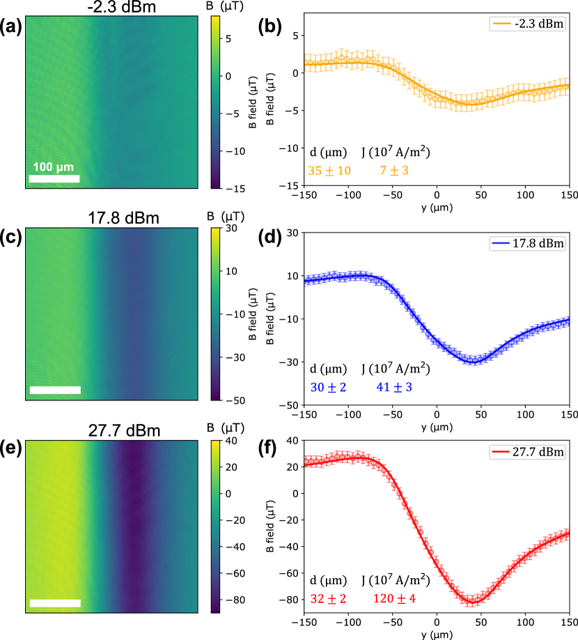
III.2 Dynamic range
To study the dynamic range accessible with the protocol developed here, we perform the same wide-field Rabi measurements for different MW power in the DUT, ranging from -2.3 dBm to 27.7 dB, with all the other same nominal experimental conditions. The results obtained through Eq. 2 are shown in Fig. 3(a), (c) and (e) for respectively -2.3, 17.8, and 27.7 dBm MW power in the DUT. Figures 3(b), (d) and (f) show the magnetic field data along a line-cut perpendicular to the strip-line fit with the theoretical model. From the fitting parameters we can notice that the resulting stand-off distance is consistent in all three separate measurements. Moreover, it can be observed that the ratios between the estimated current densities are consistent with the ratios of the input power, thus proving the good quality of the magnetic field measurement. We emphasize that in this experiment, the DUT is driven with significantly weaker MW power compared to the MW loop. At higher power levels, as shown in the SI[29], the DUT is capable of driving Rabi oscillations on its own. However, the primary aim of this work is to develop a differential Rabi imaging technique to detect weak MW signals and show how it allows to extend the MW power range that can be detected.
III.3 Magnetic field sensitivity
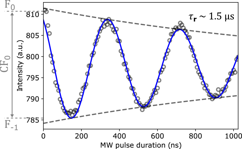
To estimate the magnetic field sensitivity we firstly calculate the shot-noise limited sensitivity through the following equation [31]:
| (3) |
with , , and being respectively the fluorescence of the bright state , the contrast and the decay time of the Rabi oscillation as shown in Fig. 4. For the typical values of these parameters we have in our experiment we obtain the value for the shot noise limited sensitivity of 670 nT Hz-1/2. We can also estimate the measured sensitivity through the full experimental Rabi oscillation defined as , where is the smallest measurable magnetic field while is the total measurement time. We estimate as the minimum measurable change in the Rabi frequency in , i.e. the standard deviation of the Rabi fit for . The value we extract from our data set is T that combined with the total measurement time of s lead to T Hz-1/2. As expected, this value is larger than the shot-noise limited sensitivity as it is evaluated from the measurement of a full Rabi oscillation. Eq. 3 instead results from fixing the MW pulse duration relative to the point of maximal slope in the Rabi oscillation, that leads to the maximal change in fluorescence following a magnetic field variation, thus resulting in optimal sensitivity[32]. A better comparison can be obtained by considering that the total measurement time , where is the number of points acquired during the measurement of a full Rabi oscillation, and is the measurement time of a single point, which is limited by the camera frame rate. After normalizing by the number of points we obtain a per-point magnetic field sensitivity 0.7 T Hz-1/2 which is comparable with the shot noise limited sensitivity.
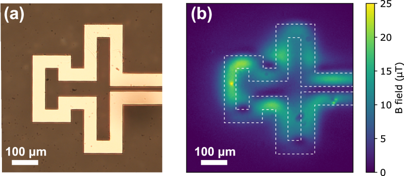
III.4 MW magnetic imaging of nontrivial DUT
In this section we demonstrate the MW imaging capabilities of the differential Rabi protocol developed in this work with another type of nontrivial DUT. The new DUT consists of a 50 m wide, 200 nm thick copper microstructure, deposited on a Al2O3 substrate in the shape shown in Fig. 5(a). The result for the MW magnetic field imaging obtained with the differential Rabi protocol when the DUT is operated at 17.8 dBm is shown in Fig. 5(b).
IV Conclusion
In conclusion, we have demonstrated the adaptability of NV centers in diamond for wide-field imaging of high-frequency ( GHz) MW magnetic fields. Compared to previous results, our work expands NV-based magnetic field imaging as it is not limited to static or low-frequency fields or to image MW devices directly used to drive the NV spins transitions. With our measurement protocol based on detection of Rabi oscillations, we have successfully mapped MW magnetic field with m-scale spatial resolution over a 340×340 m2 FOV, with a demonstrated per-pixel sensitivity of a few T Hz-1/2. This work establishes a novel procedure to use NV quantum sensing to perform wide-field imaging of high-frequency magnetic fields, and demonstrates that the here developed differential Rabi imaging technique allows to gain additional range of detectable MW power. In particular, the MW field generated by the DUT can be directly measured without the aid of the differential measurement - i.e. without using the MW loop to drive the Rabi oscillations - when it is operated at a power of 40 dBm, as reported in the SI[29]. The differential Rabi technique instead allows to measure the MW field generated by the DUT for input MW power down to dBm. This experiment proves that the differential Rabi imaging technique expands the range of detectable MW power by 40 dB. The ability we developed to image a DUT which MW field is not directly driving the NV Rabi oscillation widens the range of applicable samples and devices for MW magnetic field imaging. These results could pave the way for groundbreaking applications in NV wide-field MW fields imaging of quantum devices and materials. Future work that will further improve the impact of this technique may include for instance vector magnetometry[33], and a more elaborate engineering of the MW loop to achieve a uniform MW field direction and amplitude in the FOV. The latter will open the possibility of more advanced pulse sequences, such as double quantum protocols[34, 35].
Acknowledgements
We thank George Burns, Michael Titze, Shei Sia Su, and Edward Bielejec (Ion Beam Laboratory, Sandia National Laboratories) for help with diamond preparation. This material is based upon work supported by the U.S. Department of Energy, Office of Science, National Quantum Information Science Research Centers, Quantum Systems Accelerator. Sandia National Laboratories is a multi-mission laboratory managed and operated by National Technology and Engineering Solutions of Sandia, LLC, a wholly owned subsidiary of Honeywell International, Inc., for the DOE’s National Nuclear Security Administration under contract DE-NA0003525. This work was funded, in part, by the Laboratory Directed Research and Development Program and performed, in part, at the Center for Integrated Nanotechnologies, an Office of Science User Facility operated for the U.S. Department of Energy (DOE) Office of Science. This paper describes objective technical results and analysis. Any subjective views or opinions that might be expressed in the paper do not necessarily represent the views of the U.S. Department of Energy or the United States Government.Additionally, this research was developed with funding from the Defense Advanced Research Projects Agency (DARPA). The views, opinions and/or findings expressed are those of the author and should not be interpreted as representing the official views or policies of the Department of Defense or the U.S. Government. Distribution Statement “A” (Approved for Public Release, Distribution Unlimited).
References
References
- Van der Sar et al. [2015] T. Van der Sar, F. Casola, R. Walsworth, and A. Yacoby, “Nanometre-scale probing of spin waves using single electron spins,” Nature communications 6, 7886 (2015).
- Balents [2010] L. Balents, “Spin liquids in frustrated magnets,” nature 464, 199–208 (2010).
- Dasika, Parashar, and Saha [2023] S. Dasika, M. Parashar, and K. Saha, “Mapping ac susceptibility with quantum diamond microscope,” Rev. Sci. Instrum. 94 (2023).
- Hall, Simpson, and Hollenberg [2013] L. Hall, D. Simpson, and L. Hollenberg, “Nanoscale sensing and imaging in biology using the nitrogen-vacancy center in diamond,” Mrs Bulletin 38, 162–167 (2013).
- Sayil, Kerns, and Kerns [2005] S. Sayil, D. V. Kerns, and S. E. Kerns, “Comparison of contactless measurement and testing techniques to a all-silicon optical test and characterization method,” IEEE Transactions on Instrumentation and Measurement 54, 2082–2089 (2005).
- Rosner and Van Der Weide [2002] B. T. Rosner and D. W. Van Der Weide, “High-frequency near-field microscopy,” Review of Scientific Instruments 73, 2505–2525 (2002).
- Robertson and Lucyszyn [2001] I. D. Robertson and S. Lucyszyn, RFIC and MMIC Design and Technology, 13 (Iet, 2001).
- DiCarlo et al. [2009] L. DiCarlo, J. M. Chow, J. M. Gambetta, L. S. Bishop, B. R. Johnson, D. Schuster, J. Majer, A. Blais, L. Frunzio, S. Girvin, et al., “Demonstration of two-qubit algorithms with a superconducting quantum processor,” Nature 460, 240–244 (2009).
- Wallraff et al. [2004] A. Wallraff, D. I. Schuster, A. Blais, L. Frunzio, R.-S. Huang, J. Majer, S. Kumar, S. M. Girvin, and R. J. Schoelkopf, “Strong coupling of a single photon to a superconducting qubit using circuit quantum electrodynamics,” Nature 431, 162–167 (2004).
- Raimond, Brune, and Haroche [2001] J.-M. Raimond, M. Brune, and S. Haroche, “Manipulating quantum entanglement with atoms and photons in a cavity,” Reviews of Modern Physics 73, 565 (2001).
- You and Nori [2011] J.-Q. You and F. Nori, “Atomic physics and quantum optics using superconducting circuits,” Nature 474, 589–597 (2011).
- Aude Craik et al. [2017] D. Aude Craik, N. Linke, M. Sepiol, T. Harty, J. Goodwin, C. Ballance, D. Stacey, A. Steane, D. Lucas, and D. Allcock, “High-fidelity spatial and polarization addressing of ca+ 43 qubits using near-field microwave control,” Phys. Rev. A 95, 022337 (2017).
- Böhi et al. [2010] P. Böhi, M. F. Riedel, T. W. Hänsch, and P. Treutlein, “Imaging of microwave fields using ultracold atoms,” Applied Physics Letters 97 (2010).
- Schirhagl et al. [2014] R. Schirhagl, K. Chang, M. Loretz, and C. L. Degen, “Nitrogen-vacancy centers in diamond: Nanoscale sensors for physics and biology,” Annual Review of Physical Chemistry 65, 83–105 (2014).
- Levine et al. [2019] E. V. Levine, M. J. Turner, P. Kehayias, C. A. Hart, N. Langellier, R. Trubko, D. R. Glenn, R. R. Fu, and R. L. Walsworth, “Principles and techniques of the quantum diamond microscope,” Nanophotonics 8, 1945–1973 (2019).
- Doherty et al. [2012] M. W. Doherty, F. Dolde, H. Fedder, F. Jelezko, J. Wrachtrup, N. B. Manson, and L. C. L. Hollenberg, “Theory of the ground-state spin of the nv- center in diamond,” Phys. Rev. B 85, 205203 (2012).
- Hong et al. [2013] S. Hong, M. S. Grinolds, L. M. Pham, D. Le Sage, L. Luan, R. L. Walsworth, and A. Yacoby, “Nanoscale magnetometry with nv centers in diamond,” MRS bulletin 38, 155–161 (2013).
- Ku et al. [2020] M. J. Ku, T. X. Zhou, Q. Li, Y. J. Shin, J. K. Shi, C. Burch, L. E. Anderson, A. T. Pierce, Y. Xie, A. Hamo, et al., “Imaging viscous flow of the dirac fluid in graphene,” Nature 583, 537–541 (2020).
- Basso et al. [2022] L. Basso, P. Kehayias, J. Henshaw, M. S. Ziabari, H. Byeon, M. P. Lilly, E. Bussmann, D. M. Campbell, S. Misra, and A. M. Mounce, “Electric current paths in a si: P delta-doped device imaged by nitrogen-vacancy diamond magnetic microscopy,” Nanotechnology 34, 015001 (2022).
- Simpson et al. [2016] D. A. Simpson, J.-P. Tetienne, J. M. McCoey, K. Ganesan, L. T. Hall, S. Petrou, R. E. Scholten, and L. C. Hollenberg, “Magneto-optical imaging of thin magnetic films using spins in diamond,” Scientific reports 6, 22797 (2016).
- Kehayias et al. [2020] P. Kehayias, E. Bussmann, T. M. Lu, and A. M. Mounce, “A physically unclonable function using nv diamond magnetometry and micromagnet arrays,” J. Appl. Phys. 127, 203904 (2020).
- Kehayias et al. [2023] P. Kehayias, J. Walraven, A. Rodarte, and A. Mounce, “High-resolution short-circuit fault localization in a multilayer integrated circuit using a quantum diamond microscope,” Physical Review Applied 20, 014036 (2023).
- Kehayias et al. [2022] P. Kehayias, E. V. Levine, L. Basso, J. Henshaw, M. Saleh Ziabari, M. Titze, R. Haltli, J. Okoro, D. R. Tibbetts, D. M. Udoni, E. Bielejec, M. P. Lilly, T.-M. Lu, P. D. D. Schwindt, and A. M. Mounce, “Measurement and simulation of the magnetic fields from a 555 timer integrated circuit using a quantum diamond microscope and finite-element analysis,” Phys. Rev. Applied 17, 014021 (2022).
- Arai et al. [2022] K. Arai, A. Kuwahata, D. Nishitani, I. Fujisaki, R. Matsuki, Y. Nishio, Z. Xin, X. Cao, Y. Hatano, S. Onoda, et al., “Millimetre-scale magnetocardiography of living rats with thoracotomy,” Communications Physics 5, 200 (2022).
- Fescenko et al. [2019] I. Fescenko, A. Laraoui, J. Smits, N. Mosavian, P. Kehayias, J. Seto, L. Bougas, A. Jarmola, and V. M. Acosta, “Diamond magnetic microscopy of malarial hemozoin nanocrystals,” Physical review applied 11, 034029 (2019).
- Horsley et al. [2018] A. Horsley, P. Appel, J. Wolters, J. Achard, A. Tallaire, P. Maletinsky, and P. Treutlein, “Microwave device characterization using a widefield diamond microscope,” Phys. Rev. Appl. 10, 044039 (2018).
- Wang et al. [2015] P. Wang, Z. Yuan, P. Huang, X. Rong, M. Wang, X. Xu, C. Duan, C. Ju, F. Shi, and J. Du, “High-resolution vector microwave magnetometry based on solid-state spins in diamond,” Nature communications 6, 6631 (2015).
- Appel et al. [2015] P. Appel, M. Ganzhorn, E. Neu, and P. Maletinsky, “Nanoscale microwave imaging with a single electron spin in diamond,” New J. Phys. 17, 112001 (2015).
- [29] Additional details are included in the supplemental material.
- Magaletti et al. [2024] S. Magaletti, L. Mayer, J.-F. Roch, and T. Debuisschert, “Modelling rabi oscillations for widefield radiofrequency imaging in nitrogen-vacancy centers in diamond,” New J. Phys. 26, 023020 (2024).
- Taylor et al. [2008] J. M. Taylor, P. Cappellaro, L. Childress, L. Jiang, D. Budker, P. R. Hemmer, A. Yacoby, R. Walsworth, and M. D. Lukin, “High-sensitivity diamond magnetometer with nanoscale resolution,” Nat. Phys. 4, 810–816 (2008).
- Rondin et al. [2014] L. Rondin, J.-P. Tetienne, T. Hingan, J.-F. Roch, P. Maletinsky, and V. Jacques, “Magnetometry with nitrogen-vacancy defects in diamond,” Rep. Prog. Phys. 77, 056503 (2014).
- Chen et al. [2020] B. Chen, X. Hou, F. Ge, X. Zhang, Y. Ji, H. Li, P. Qian, Y. Wang, N. Xu, and J. Du, “Calibration-free vector magnetometry using nitrogen-vacancy center in diamond integrated with optical vortex beam,” Nano Letters 20, 8267–8272 (2020).
- Kazi et al. [2021] Z. Kazi, I. M. Shelby, H. Watanabe, K. M. Itoh, V. Shutthanandan, P. A. Wiggins, and K.-M. C. Fu, “Wide-field dynamic magnetic microscopy using double-double quantum driving of a diamond defect ensemble,” Phys. Rev. Appl. 15, 054032 (2021).
- Hart et al. [2021] C. A. Hart, J. M. Schloss, M. J. Turner, P. J. Scheidegger, E. Bauch, and R. L. Walsworth, “N-v–diamond magnetic microscopy using a double quantum 4-ramsey protocol,” Phys. Rev. Appl. 15, 044020 (2021).