Universal Model of Optical-Field Electron Tunneling from Two-Dimensional Materials
Abstract
We develop analytical models of optical-field electron tunneling from the edge and surface of two-dimensional (2D) materials, including the effects of reduced dimensionality, non-parabolic energy dispersion, band anisotropy, quasi-time dependent tunneling and emission dynamics indueced by the laser field. We discover a universal scaling between the tunneling current density and the laser electric field : In( with in the edge emission and in the vertical surface emission, which both are distinctive from the traditional Fowler-Nordheim (FN) model of . The current density exhibits an unexpected high-field saturation effect due to the reduced dimensionality of 2D materials, which is completely different from the space-charge saturation commonly observed in traditional bulk materials. Our results reveal the dc bias as an efficient method in modulating the optical-field tunneling sub-optical-cycle emission characteristics. Importantly, our model is in excellent agreement with a recent experiment on graphene. Our findings offer a theoretical foundation for the understanding of optical-field tunneling emission from the 2D material system, which is useful for the development of 2D-material based optoelectronics and vacuum nanoelectronics
Introduction.—Laser-matter interaction offers the capability for the manipulation of electron excitation and dynamics at ultrashort timescale, such as high-order harmonic generation [1, 2], carrier interband transition [3], spontaneous radiation [4], photoelectron emission [5, 6, 7, 8, 9, 10, 11, 12], quantum coherent control of excitation states [13, 14, 15, 16] and many others. Among them, laser-triggered photoemission from solids has gained considerable current attention, because of its crucial role in the development of high-resolution electron microscopy and diffraction [17, 18], free electron lasers [19], tabletop laser accelerators [20], coherent electron sources [21, 22] and quantum nano-vacuum electronics [23, 24, 25, 26].
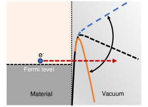
At high laser intensity, the photoemission is due to the optical-field electron tunneling process (or optical-field emission) [27, 28], where the strong time-varying light field greatly suppresses the material interface potential barrier enabling electron tunneling in the vicinity of Fermi level (cf. Fig. 1). In this non-perturbative field-driven near-transient tunneling regime, incident optical electric field can achieve the steering of electron motion at a sub-cycle temporal scale, such as the subfemtosecond tunneling [29, 30] and attosecond electron pulse generation [31], which makes optical-field tunneling emission is important for ultrafast optical-field-driven electronics [32] and on-chip attosecond lightwave science [33, 34].
Other than metallic nanostrucutres [8, 10, 27, 35, 36, 37, 38], emerging two-dimensional (2D) materials [39, 40, 41, 42, 43] are employed to study their optical-field photoemission as well, due to the distinctive electronic band structures and nanoscale sharpness which provide the huge localized field enhancement factor allowing sufficient electron emission in using low-power lasers. For instance, the most common 2D material graphene has the atomic-scale thickness resulting in significantly high field enhancement near the edge [44], large electron mobility [45] and high thermal damage threshold [46], which explains graphene being used effectively to realize ultrafast optical-field electron tunneling emission [40]. Despite tremendous ongoing efforts to implement 2D materials as emitters for ultrafast applications, the theoretical description of 2D material electron emission relies heavily on the Fowler-Nordheim (FN) formalism (which was developed for the traditional bulk materials) that is fundamentally incompatible with the reduced dimensionality and electronic properties of 2D materials [47, 48, 49, 50, 51, 52, 53, 54]. The optical-field tunneling model of 2D materials thus remains an urgent and open question that has yet to be addressed.
In this work, we develop universal models for optical-field tunneling emission from the edge and surface of a wide class of 2D materials, which explicitly considers the reduction of dimensionality, non-parabolic energy dispersion of 2D material, quasi-time dependent tunneling and electron emission dynamics driven by ultrafast laser. We reveal a universal current-field scaling: In( with for the edge emission and = 1 for the vertical surface emission respectively, which are different from the conventional FN law of [55]. A peculiar saturation of photocurrent at ultrahigh laser intensity is identified due to the reduced dimensionality. Importantly, our model is in an excellent agreement to a recent experiment [40] of optical-field emission from monolayer graphene over different combinations of dc and laser fields. Our model provides a universal description of optical-field tunnelling phenomena for a wide variety of 2D materials and shall form an important foundation for the development of novel 2D-material based ultrafast optical-field-driven tunneling nano-vacuum optoelectronics and device engineering.
Theoretical formalism.—We consider a 2D material lying in the plane with a dc field under the illumination of a laser field perpendicular to the edge. The optical-field-induced tunneling current density via the edge along direction is [50, 49]
| (1) |
where is the electron charge, is the spin-valley degeneracy factor, and are the electron wavevector and energy component in the plane, respectively. Here, is the electron -direction velocity ( is the reduced Planck constant), is the zero-temperature Fermi-Dirac distribution function, is the time-dependent electron transmission probability through the edge at energy component [cf. Eq. (3)], denotes the discrete bound states along the direction orthogonal to the plane, due to the confinement of electrons within the 2D plane, and denotes the summation of all these discrete bound states.
Consider a 2D material with a general form of anisotroppic energy dispersion,
| (2) |
where and are the material-dependent parameters along and directions respectively, and . Using Eq. (2), we derive , and , where denotes the Heaviside function.
![[Uncaptioned image]](https://cdn.awesomepapers.org/papers/64a6879e-4aa2-4c2a-b6b5-42e323058ea0/x2.png)
In the optical high-field tunneling regime, incident optical field primarily behaves like an ac electric field that modulates the barrier, in which the effects of photoexcited nonthermal electrons can be ignored [40, 7]. Thus, the optical-field tunneling through the barrier resembles instantaneous field emission as a function of laser field, and the time-dependent transmission probability is approximated at quasi-static limit based on the Wentzel-Kramers-Brillouin (WKB) method, which gives
| (3) |
Here, is the summation of the dc field and the time-dependent optical field , and denotes the Heaviside function to ensure electron emission occurs only during the negative field cycles. We omit in the expressions below for simplicity. The tunneling factor is , where , is the work function, is the Fermi energy, and is the free-electron mass. Substituting Eq. (3) into Eq. (1) yields the optical-field edge tunneling current density, , where , and is a complex integral as shown in Eq. (S4) in the Supplemental Materials (SM). In optical-field tunneling, the emission electrons are mostly located near the Fermi level: , thus . Under this approximation, the tunneling current can be analytically solved as (see Sec. I in the SM for details)
![[Uncaptioned image]](https://cdn.awesomepapers.org/papers/64a6879e-4aa2-4c2a-b6b5-42e323058ea0/x3.png)
| (4) |
where , is with , is the modified Bessel function of the first kind, is the modified Struve function, , , is the complete gamma function, , and (including , and below) all are -dependent constants, and is the generalized hypergeometric function. The details of the constants and other parameters can be found in Sec. I in the SM.
The universal analytical [Eq. (4)] is characterized for three classes of the 2D materials [ = 1, odd and even ], which shows good agreements with the numerical results from Eq. (S4) (cf. Fig. S1). Equation (4) also indicates that is independent of the material parameter , and thus a possible universal edge emission scaling. At the practical field regime () and the ultrahigh field regimes (), the analytical results for the universal model and three representative 2D systems are summarized in Table 1 (see Sec. II in the SM for detailed derivations). The validity of these analytical equations are verified in Fig. S2 in the SM.
Intriguingly, at practical intensity regime (column 2 of Table 1), the prefactor () of the field strength exhibits an unconventional universal scaling of with for , which is in stark contrast to of the conventinoal FN law [55] derived for traditional 3D bulk materials. Interestingly, the same universal scaling has also been reported in the current-temperature scaling of the thermionic emission for lateral 2D-material-based Schottky contacts [49]. At ultrahigh field regime (column 3 of Table 1), saturates and becomes independent of field strength (or ). Such saturation reveals a dramatic consequence of the reduced dimensional of 2D material, in which the emission current saturates due to limited availability of electrons. Such a source-limited emission behavior [56] is completely different from the space-charge limitation of traditional bulk materials [24, 25], and shall offer a distinctive high-field transport signature of 2D-material-based electron optical-field emitters.
Optical-field tunenling from 2D material surface.—We now consider the case of optical-field tunneling of electrons that occurs vertically from the plane of the 2D materials. In this case, the dc field and high-intensity optical field are considered to be perpendicular to the 2D surface. During this out-of-plane tunneling process, carrier scattering effects, such as electron-electron [57] and defects scatterings [58], violates the conservation of in-plane momentum , which leads to the coupling between and . Thus, the vertical optical-field tunneling current density from 2D material surface is expressed as [49],
| (5) |
where is the thickness of 2D material and is the cross-plane group velocity of the electron with discrete energy state . Consider the surface tunneling from one subband near the Fermi level, Eq. (5) becomes
| (6) |
where is the density of state (DOS), and and are defined in Eq. (3).
Employing a general 2D anisotropic DOS with being material-dependent coefficients and [54], Eq. (6) yields a generalized analytical form
| (7) |
where , and and are the complete gamma function and the upper incomplete gamma function respectively. By taking the Taylor series expansion of for and , is solved under these two limits for the universal formula and three different materials in Table 2 (see Sec. III of the SM for more details).
The vertical surface optical-field emission current all converge to an universal scaling of In( with at the practical field regime, which is different from of edge emission presented in Table 1 and of the classical FN law. The current also saturates at the ultrahigh intensity due to the reduced dimensionality. The validity of these analytical solutions is shown in Fig. S3 in the SM. By comparing Figs. S2 and S3, it is found under the same illumination condition, vertical surface optical-field tunneling generates significantly higher emission current than the edge tunneling. Notably the analytical formulas in this work can be directly employed to study dc field emission by replacing with dc field .
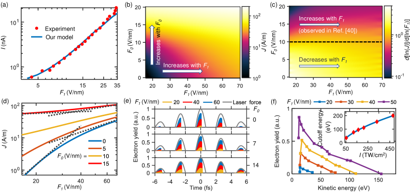
Current-field characteristics.—We verify our model in comparison with a recently measured optical-field tunneling emission current from the edge of monolayer graphene [40] as shown in Fig. 2(a). Due to the significantly low backscattering efficiency on the carbon surface [59], the contributions from rescattered electrons are excluded in the calculations of Fig. 2 (see Sec. IV of the SM for the method). Our model produces a good agreement with the experiment by using the dc and laser field enhancement factors of about 146 and 22 respectively, which are smaller than the reported values [40] based on the traditional bulk material FN law.
The optical-field edge emission current density from the graphene and its power dependence on the laser field are calculated as a function of laser field and dc field in Fig. 2(b) and 2(c), respectively. A Gaussian laser pulse is chosen, , where is the peak of field strength, is the pulse width, and is the angular frequency. The laser wavelength is 800 nm with a pulse width of = 8 fs (3 cycles) and the integration time [cf. Eq. (S40)] is from -30 to 30 fs. Increasing either laser intensity or dc bias will increase the optical-field emission [cf. Fig. 2(b)]. Interestingly, increasing changes the order of nonlinear power dependence of on from the decreasing to increasing trends [cf. Fig. 2(c) and dotted lines in Fig.2(d)]. This transition occurs at around V/nm and exists in the case without the consideration of emitted electron dynamics in the vacuum. Such behavior arises from the having higher electron tunneling probability through the barrier with stronger dc bias, thus allowing relatively more electrons to contribute in the high-intensity regime. When the relative number of emitted electrons is sufficiently large, the unconventional increasing exponential growth rate of current with laser intensity takes place [cf. the case with V/nm as shown in Fig. 2(c)]. This nonlinear order increment is also in agreement with experimental observations [40].
Sub-cycle electron emission characteristics.—The time-dependent optical-field emission current [cf. Eq. (S40)] in Fig. 2(e) shows that most electrons are emitted during the negative first half cycles due to the attainment of sufficient kinetic energy to escape the confinement of positive optical cycle. Beacsue of the reduced kinetic energy, parts of the electrons emitted in the negative second half cycles can be driven back to the edge by the deceleration of following positive cycle. This confirms the sub-optical-cycle emission dynamics in the optical-field emission regime. Increasing the dc field enlarges the rescattering time (cf. the sharp edge of emission yield), which implies that under the stronger dc acceleration, more electrons could escape the laser field and contribute to the net photocurrent. Finally, we calculate the kinetic energy spectra at the position of around 25 nm away from the graphene edge for different laser field at zero dc field ( = 0). The extracted main spectrum peaks are plotted in Fig. 2(f). The cutoff kinetic energy representing the maximum kinetic energy of collected photoelectron as a function of laser intensity is depicted in the inset of Fig. 2(f). The sublinear dependence of the cutoff energy on the laser intensity indicates a sub-cycle-timescale electron emission characteristics [60] and the electron dynamic motion can be controlled by the optical field strength.
Conclusion.—In summary, we have presented analytical and universal models for ultrafast optical-field tunneling emission of electrons from the edge and surface of general anisotropic 2D materials.
Our model reports a universal scaling between the optical tunneling current density and laser electric field strength given by with = 3/2 in the edge emission and = 1 in the vertical surface emission, which both are different from the traditional scaling of based on the FN law.
At ultrahigh laser field, we observe a saturation effect that the tunneling current no longer depends on the field, due to the reduction of dimensionality.
These universal scaling and saturation are explicitly exhibited in three selected materials: monolayer grapehene, highly doped multilayer black phosphorus and -stacked trilayer grapehene.
Our calculation also well reproduces prior experimental measurement, and uncovers the dc induced modulation to the optical-field emission current and the power-dependence of photocurrent on laser field.
The developed analytical formulation provides a theoretical foundation for understanding a broad range of 2D materials in applications related to ultrafast optical-field-driven optoelectronics and field emission in vaccum nanoelectronics.
The model shall pave a way towards a generalized model combining thermal, field and photoemission [61] for 2D materials which is highly desirable for the design of 2D-material-based electron emitter.
This work is supported by the Singapore A*STAR IRG grant (A2083c0057). Y.S.A. is supported by the Singapore Ministry of Education (MOE) Academic Research Fund (AcRF) Tier 2 under Grant No. MOE-T2EP50221-0019.
References
- Ghimire et al. [2011] S. Ghimire, A. D. DiChiara, E. Sistrunk, P. Agostini, L. F. DiMauro, and D. A. Reis, Observation of high-order harmonic generation in a bulk crystal, Nature physics 7, 138 (2011).
- Liu et al. [2017] H. Liu, Y. Li, Y. S. You, S. Ghimire, T. F. Heinz, and D. A. Reis, High-harmonic generation from an atomically thin semiconductor, Nature Physics 13, 262 (2017).
- Schultze et al. [2014] M. Schultze, K. Ramasesha, C. Pemmaraju, S. Sato, D. Whitmore, A. Gandman, J. S. Prell, L. Borja, D. Prendergast, K. Yabana, et al., Attosecond band-gap dynamics in silicon, Science 346, 1348 (2014).
- Rakhmatov et al. [2020] E. Rakhmatov, A. Alizadehkhaledi, G. Hajisalem, and R. Gordon, Bright upconverted emission from light-induced inelastic tunneling, Optics Express 28, 16497 (2020).
- Hommelhoff et al. [2006] P. Hommelhoff, C. Kealhofer, and M. A. Kasevich, Ultrafast electron pulses from a tungsten tip triggered by low-power femtosecond laser pulses, Physical review letters 97, 247402 (2006).
- Ropers et al. [2007] C. Ropers, D. Solli, C. Schulz, C. Lienau, and T. Elsaesser, Localized multiphoton emission of femtosecond electron pulses from metal nanotips, Physical review letters 98, 043907 (2007).
- Wu and Ang [2008] L. Wu and L. Ang, Nonequilibrium model of ultrafast laser-induced electron photofield emission from a dc-biased metallic surface, Physical Review B 78, 224112 (2008).
- Krüger et al. [2011] M. Krüger, M. Schenk, and P. Hommelhoff, Attosecond control of electrons emitted from a nanoscale metal tip, Nature 475, 78 (2011).
- Pant and Ang [2012] M. Pant and L. Ang, Ultrafast laser-induced electron emission from multiphoton to optical tunneling, Physical Review B 86, 045423 (2012).
- Dombi et al. [2013] P. Dombi, A. Hörl, P. Rácz, I. Márton, A. Trügler, J. R. Krenn, and U. Hohenester, Ultrafast strong-field photoemission from plasmonic nanoparticles, Nano letters 13, 674 (2013).
- Pant and Ang [2013] M. Pant and L. Ang, Time-dependent quantum tunneling and nonequilibrium heating model for the generalized einstein photoelectric effect, Physical Review B 88, 195434 (2013).
- Zhang and Lau [2016] P. Zhang and Y. Lau, Ultrafast strong-field photoelectron emission from biased metal surfaces: exact solution to time-dependent schrödinger equation, Scientific reports 6, 1 (2016).
- Sirotti et al. [2014] F. Sirotti, N. Beaulieu, A. Bendounan, M. G. Silly, C. Chauvet, G. Malinowski, G. Fratesi, V. Véniard, and G. Onida, Multiphoton k-resolved photoemission from gold surface states with 800-nm femtosecond laser pulses, Physical Review B 90, 035401 (2014).
- Förster et al. [2016] M. Förster, T. Paschen, M. Krüger, C. Lemell, G. Wachter, F. Libisch, T. Madlener, J. Burgdörfer, and P. Hommelhoff, Two-color coherent control of femtosecond above-threshold photoemission from a tungsten nanotip, Physical Review Letters 117, 217601 (2016).
- Reutzel et al. [2019] M. Reutzel, A. Li, and H. Petek, Coherent two-dimensional multiphoton photoelectron spectroscopy of metal surfaces, Physical Review X 9, 011044 (2019).
- Zhou and Zhang [2022] Y. Zhou and P. Zhang, Unraveling quantum pathways interference in two-color coherent control of photoemission with bias voltages, Physical Review B 106, 085402 (2022).
- Sun et al. [2020] S. Sun, X. Sun, D. Bartles, E. Wozniak, J. Williams, P. Zhang, and C.-Y. Ruan, Direct imaging of plasma waves using ultrafast electron microscopy, Structural Dynamics 7, 064301 (2020).
- Sciaini and Miller [2011] G. Sciaini and R. D. Miller, Femtosecond electron diffraction: heralding the era of atomically resolved dynamics, Reports on Progress in Physics 74, 096101 (2011).
- Grguraš et al. [2012] I. Grguraš, A. R. Maier, C. Behrens, T. Mazza, T. Kelly, P. Radcliffe, S. Düsterer, A. Kazansky, N. Kabachnik, T. Tschentscher, et al., Ultrafast x-ray pulse characterization at free-electron lasers, Nature Photonics 6, 852 (2012).
- Peralta et al. [2013] E. Peralta, K. Soong, R. England, E. Colby, Z. Wu, B. Montazeri, C. McGuinness, J. McNeur, K. Leedle, D. Walz, et al., Demonstration of electron acceleration in a laser-driven dielectric microstructure, Nature 503, 91 (2013).
- Polyakov et al. [2013] A. Polyakov, C. Senft, K. Thompson, J. Feng, S. Cabrini, P. Schuck, H. Padmore, S. J. Peppernick, and W. P. Hess, Plasmon-enhanced photocathode for high brightness and high repetition rate x-ray sources, Physical review letters 110, 076802 (2013).
- Jones et al. [2016] E. Jones, M. Becker, J. Luiten, and H. Batelaan, Laser control of electron matter waves, Laser & Photonics Reviews 10, 214 (2016).
- Lin et al. [2017] J. Lin, P. Y. Wong, P. Yang, Y. Lau, W. Tang, and P. Zhang, Electric field distribution and current emission in a miniaturized geometrical diode, Journal of Applied Physics 121, 244301 (2017).
- Zhang et al. [2017] P. Zhang, Á. Valfells, L. Ang, J. Luginsland, and Y. Lau, 100 years of the physics of diodes, Applied Physics Reviews 4, 011304 (2017).
- Zhang et al. [2021] P. Zhang, Y. S. Ang, A. L. Garner, Á. Valfells, J. Luginsland, and L. Ang, Space–charge limited current in nanodiodes: Ballistic, collisional, and dynamical effects, Journal of Applied Physics 129, 100902 (2021).
- Zhou et al. [2021] S. Zhou, K. Chen, M. T. Cole, Z. Li, M. Li, J. Chen, C. Lienau, C. Li, and Q. Dai, Ultrafast electron tunneling devices—from electric-field driven to optical-field driven, Advanced Materials 33, 2101449 (2021).
- Bormann et al. [2010] R. Bormann, M. Gulde, A. Weismann, S. Yalunin, and C. Ropers, Tip-enhanced strong-field photoemission, Physical review letters 105, 147601 (2010).
- Krüger et al. [2012] M. Krüger, M. Schenk, M. Förster, and P. Hommelhoff, Attosecond physics in photoemission from a metal nanotip, Journal of Physics B: Atomic, Molecular and Optical Physics 45, 074006 (2012).
- Rybka et al. [2016] T. Rybka, M. Ludwig, M. F. Schmalz, V. Knittel, D. Brida, and A. Leitenstorfer, Sub-cycle optical phase control of nanotunnelling in the single-electron regime, Nature Photonics 10, 667 (2016).
- Ludwig et al. [2020] M. Ludwig, G. Aguirregabiria, F. Ritzkowsky, T. Rybka, D. C. Marinica, J. Aizpurua, A. G. Borisov, A. Leitenstorfer, and D. Brida, Sub-femtosecond electron transport in a nanoscale gap, Nature Physics 16, 341 (2020).
- Kim et al. [2023] H. Kim, M. Garg, S. Mandal, L. Seiffert, T. Fennel, and E. Goulielmakis, Attosecond field emission, Nature 613, 662 (2023).
- Arashida et al. [2022] Y. Arashida, H. Mogi, M. Ishikawa, I. Igarashi, A. Hatanaka, N. Umeda, J. Peng, S. Yoshida, O. Takeuchi, and H. Shigekawa, Subcycle mid-infrared electric-field-driven scanning tunneling microscopy with a time resolution higher than 30 fs, ACS Photonics 9, 3156 (2022).
- Goulielmakis et al. [2007] E. Goulielmakis, V. S. Yakovlev, A. L. Cavalieri, M. Uiberacker, V. Pervak, A. Apolonski, R. Kienberger, U. Kleineberg, and F. Krausz, Attosecond control and measurement: lightwave electronics, Science 317, 769 (2007).
- Bionta et al. [2021] M. R. Bionta, F. Ritzkowsky, M. Turchetti, Y. Yang, D. Cattozzo Mor, W. P. Putnam, F. X. Kärtner, K. K. Berggren, and P. D. Keathley, On-chip sampling of optical fields with attosecond resolution, Nature Photonics 15, 456 (2021).
- Herink et al. [2012] G. Herink, D. R. Solli, M. Gulde, and C. Ropers, Field-driven photoemission from nanostructures quenches the quiver motion, Nature 483, 190 (2012).
- Park et al. [2012] D. J. Park, B. Piglosiewicz, S. Schmidt, H. Kollmann, M. Mascheck, and C. Lienau, Strong field acceleration and steering of ultrafast electron pulses from a sharp metallic nanotip, Physical review letters 109, 244803 (2012).
- Putnam et al. [2017] W. P. Putnam, R. G. Hobbs, P. D. Keathley, K. K. Berggren, and F. X. Kärtner, Optical-field-controlled photoemission from plasmonic nanoparticles, nature physics 13, 335 (2017).
- Xiong et al. [2020] X. Xiong, Y. Zhou, Y. Luo, X. Li, M. Bosman, L. K. Ang, P. Zhang, and L. Wu, Plasmon-enhanced resonant photoemission using atomically thick dielectric coatings, ACS nano 14, 8806 (2020).
- Higuchi et al. [2017] T. Higuchi, C. Heide, K. Ullmann, H. B. Weber, and P. Hommelhoff, Light-field-driven currents in graphene, Nature 550, 224 (2017).
- Son et al. [2018] B. H. Son, H. S. Kim, J.-Y. Park, S. Lee, D. J. Park, and Y. H. Ahn, Ultrafast strong-field tunneling emission in graphene nanogaps, ACS Photonics 5, 3943 (2018).
- Zhou et al. [2019] S. Zhou, K. Chen, M. T. Cole, Z. Li, J. Chen, C. Li, and Q. Dai, Ultrafast field-emission electron sources based on nanomaterials, Advanced Materials 31, 1805845 (2019).
- Heide et al. [2019] C. Heide, T. Boolakee, T. Higuchi, H. B. Weber, and P. Hommelhoff, Interaction of carrier envelope phase-stable laser pulses with graphene: the transition from the weak-field to the strong-field regime, New Journal of Physics 21, 045003 (2019).
- Sushko et al. [2021] A. Sushko, K. De Greve, M. Phillips, B. Urbaszek, A. Y. Joe, K. Watanabe, T. Taniguchi, A. L. Efros, C. S. Hellberg, H. Park, et al., Asymmetric photoelectric effect: Auger-assisted hot hole photocurrents in transition metal dichalcogenides, Nanophotonics 10, 105 (2021).
- Weiss et al. [2012] N. O. Weiss, H. Zhou, L. Liao, Y. Liu, S. Jiang, Y. Huang, and X. Duan, Graphene: an emerging electronic material, Advanced materials 24, 5782 (2012).
- Novoselov et al. [2004] K. S. Novoselov, A. K. Geim, S. V. Morozov, D.-e. Jiang, Y. Zhang, S. V. Dubonos, I. V. Grigorieva, and A. A. Firsov, Electric field effect in atomically thin carbon films, science 306, 666 (2004).
- David et al. [2014] L. David, A. Feldman, E. Mansfield, J. Lehman, and G. Singh, Evaluating the thermal damage resistance of graphene/carbon nanotube hybrid composite coatings, Scientific reports 4, 1 (2014).
- Qin et al. [2011] X.-Z. Qin, W.-L. Wang, N.-S. Xu, Z.-B. Li, and R. G. Forbes, Analytical treatment of cold field electron emission from a nanowall emitter, including quantum confinement effects, Proceedings of the Royal Society A: Mathematical, Physical and Engineering Sciences 467, 1029 (2011).
- Ang et al. [2017] Y. Ang, S.-J. Liang, and L. Ang, Theoretical modeling of electron emission from graphene, MRS Bulletin 42, 505 (2017).
- Ang et al. [2018] Y. S. Ang, H. Y. Yang, and L. Ang, Universal scaling laws in schottky heterostructures based on two-dimensional materials, Physical review letters 121, 056802 (2018).
- Ang et al. [2019] Y. S. Ang, Y. Chen, C. Tan, and L. Ang, Generalized high-energy thermionic electron injection at graphene interface, Physical Review Applied 12, 014057 (2019).
- Ang et al. [2021] Y. S. Ang, L. Cao, and L. K. Ang, Physics of electron emission and injection in two-dimensional materials: Theory and simulation, InfoMat 3, 502 (2021).
- Chan et al. [2021] W. J. Chan, Y. S. Ang, and L. Ang, Thermal-field electron emission from three-dimensional dirac and weyl semimetals, Physical Review B 104, 245420 (2021).
- Chan et al. [2022] W. J. Chan, C. Chua, Y. S. Ang, and L. K. Ang, Field emission in emerging two-dimensional and topological materials: A perspective, IEEE Transactions on Plasma Science (2022).
- Ang et al. [2023] L. K. Ang, Y. S. Ang, and C. H. Lee, Universal model for electron thermal-field emission from two-dimensional semimetals, Physics of Plasmas 30, 033103 (2023).
- Fowler and Nordheim [1928] R. H. Fowler and L. Nordheim, Electron emission in intense electric fields, Proceedings of the Royal Society of London. Series A, Containing Papers of a Mathematical and Physical Character 119, 173 (1928).
- Chua et al. [2021] C. Chua, C. Y. Kee, Y. S. Ang, and L. Ang, Absence of space-charge-limited current in unconventional field emission, Physical Review Applied 16, 064025 (2021).
- Meshkov [1986] S. Meshkov, Tunneling of electrons from a two-dimensional channel into the bulk, Zh. Eksp. Teor. Fiz 91, 198 (1986).
- Chandni et al. [2016] U. Chandni, K. Watanabe, T. Taniguchi, and J. P. Eisenstein, Signatures of phonon and defect-assisted tunneling in planar metal–hexagonal boron nitride–graphene junctions, Nano letters 16, 7982 (2016).
- Huang et al. [2006] L. Huang, S. P. Lau, H. Yang, and S. Yu, Local measurement of secondary electron emission from zno-coated carbon nanotubes, Nanotechnology 17, 1564 (2006).
- Echternkamp et al. [2016] K. Echternkamp, G. Herink, S. V. Yalunin, K. Rademann, S. Schäfer, and C. Ropers, Strong-field photoemission in nanotip near-fields: from quiver to sub-cycle electron dynamics, Applied Physics B 122, 1 (2016).
- Jensen [2007] K. L. Jensen, General formulation of thermal, field, and photoinduced electron emission, Journal of Applied Physics 102, 024911 (2007).