-
September 2024
Tight-binding model of Pt-based jacutingaites as combination of the honeycomb and kagome lattices
Abstract
We introduce a refined tight-binding (TB) model for Pt-based jacutingaite materials PtX3, ( = Zn, Cd, Hg; X = S, Se, Te), offering a detailed representation of the low-energy physics of its monolayers. This model incorporates all elements with significant spin-orbit coupling contributions, which are essential for understanding the topological energy gaps in these materials. Through comparison with first-principles calculations, we meticulously fitted the TB parameters, ensuring an accurate depiction of the energy bands near the Fermi level. Our model reveals the intricate interplay between the Pt and metal orbitals, forming distinct kagome and honeycomb lattice structures. Applying this model, we explore the edge states of Pt-based jacutingaite monolayer nanoribbons, highlighting the sensitivity of the topological edge states dispersion bands to the nanostructures geometric configurations. These insights not only deepen our understanding of jacutingaite materials but also assist in tailoring their electronic properties for future applications.
1 Introduction
The successful synthesis of graphene [1], coupled with the discovery of its remarkable properties, has spurred extensive research on the properties and unique characteristics of novel two-dimensional (2D) materials [2, 3, 4, 5, 6]. The investigation of alternative 2D materials, such as enes (X = Si, Ge, Sn), transition metal dichalcogenides, and black phosphorus, has revealed a variety of unique properties and energy gaps, providing superior control over the electronic behavior and transport [7, 8, 9, 10, 11, 12]. Moreover, materials exhibiting intrinsic spin-orbit coupling (SOC) energy gaps leading to the Quantum spin Hall (QSH) effect have drawn great attention. This effect is characterized by a Z2 topological invariant distinguishing these materials from ordinary insulators. The emergence of such topological states implies a paradigm shift with implications for spintronics [13, 14, 15, 16, 17, 18]. Inherently resistant to backscattering from various perturbations, these states pave the way for robust, non-dissipative charge transport and innovative applications in quantum computing and photonics [13, 19, 20]. The concept of QSH states, initially theorized for graphene by Kane and Mele [21], found empirical evidence in HgTe/CdTe and InAs/GaSb quantum wells [22, 23]. These states, protected by time-reversal symmetry, are robust against non-magnetic perturbations. A notable realization of such topological systems is the jacutingaite (Pt2HgSe3, Z) monolayer [24], approximated as a honeycomb structure of Hg elements.
The jacutingaite is a new species of platinum-group mineral discovered at the Cauê iron-ore deposit, Itabira district, Minas Gerais, Brazil, in 2008 [25], and then synthesized in 2012 [26]. The ore is brittle, highly stable, with an excellent cleavage 001, whose perpendicular direction is composed of layers stacked by van der Waals interaction in an AA configuration [26]. In its bulk form, the jacutingaite is a hexagonal structure that exhibits dual-topological semi-metal characteristics, combining a weak QSH phase and mirror-protected topological crystalline phase [27, 28]. In its monolayer form manifests as a QSH topological semiconductor [29, 24], as evidenced by a measured topological gap of 110 meV and decay of edge states into the bulk over approximately 5 Å [24]. The jacutingaite monolayer is the most promising material to host QSH states similarly to the original proposal for graphene described by Kane-Mele model, given its structural stability and large topological gap [29, 24, 20, 30] .
The jacutingaite monolayer family ( Ni, Pd, Pt; Zn, Cd, Hg; S, Se, Te) were theoretically presented by de LIMA, F. et al., 2020 [31]. They demonstrated that there are other jacutingaite like structures that also host the Kane-Mele QSH state. Relevant for top-down mode synthesis, they also demonstrated that the bulk structure presents cleavage energies at the level of other experimentally exfoliable materials, in the range of 0.22 J/m2 – 0.85 J/m2 [31]. From this family, one group that we can highlight are those that present a energy gap and Kane-Mele QSH state, the Pt-based jacutingaites.
Distinct from graphene, the dispersion is only approximately linear from the K(K′)– directions, whereas along the K(K′)–M direction it is almost flat. The traditional Kane-Mele model inadequately captures these low-energy characteristics of jacutingaite monolayers, requiring a more nuanced approach for accurate representation.
This work investigates the Pt-based jacutingaite monolayers (Pt, N= Zn, Cd, Hg; X= S, Se, Te) and introduces an advanced tight-binding (TB) model derived from density functional theory (DFT) band structures. Predicted as QSH topological semiconductors with substantial SOC band gaps [31], these monolayers are modeled considering all SOC-contributing elements and their respective lattices, comprising a honeycomb and a kagome lattice superposition. Furthermore, we incorporate real next-nearest-neighbor (NNN) hopping terms and all hopping terms within a radius equivalent to the NNN distance to the N sites, which form the basis of the Kane-Mele model. Our refined TB model exhibits excellent agreement with first-principles calculations across a broad spectrum of wavevectors and energies around the Fermi level, promising enhanced understanding of these fascinating materials.
2 Methodology
2.1 Tight Binding Model for jacutingaite-like systems
The crystal structure of jacutingaite (, ) has space group [25, 26]. The Pt-based jacutingaite monolayer and Wyckoff position of their elements are illustrated in Figure 1, where . The electronic characteristics of jacutingaite-family materials can be understood by taking into account their structure, which, with respect to the low-lying bands can be described as two interpenetrating honeycomb and kagome sub-lattices.

Jacutingaite-type systems have structural and electronic characteristics of both types of lattices. Thus, we propose a TB model that combines these two sub-lattices, i.e., a honeycomb-kagome (HK) structure, in order to obtain a better agreement with the DFT energy bands near the SOC energy gap, in comparison with the pure Kane-Mele model.
As shown in the next section the orbitals that contribute most significantly to the conduction and valence bands around the topological energy gap are S1/2 orbitals from metal e 5D5/2 orbitals from Pt . By taking into account only these elements, one can visualize (see Figure 2) the jacutingaite-like structure as a honeycomb buckled lattice, resembling the silicene or germanene structure, composed of metals and a planar kagome lattice formed by the Pt elements.

In Figure 3 (a) the dotted lines connecting metals form the hexagons of a honeycomb lattice. The region highlighted by the black solid contour depicts a unit cell, showing that two metals per cell occupy non-equivalent sites, which are labeled as and . We considered the on-site energy, nearest-neighbor (NN) and NNN hopping parameters as indicated by the arrows, as well as the SOC for the construction of the corresponding Hamiltonian term based on the buckled sub-lattice formed by metals.
In Figure 3 (b) the dotted lines connecting the Pt elements form a triangular geometry with an arrangement of interconnected hexagons. There are three Pt elements per cell occupying non-equivalent sites, which are labeled as , and . As in the previous case, we included an on-site energy, NN and NNN hopping parameters and SOC, as indicated by the arrows, for the construction of the Hamiltonian term for the planar sub-lattice formed by Pt elements.

Figure 3 (c) depicts the system as two interpenetrating honeycomb buckled and kagome planar sub-lattices. Thus, we considered the NN and NNN hopping parameters as indicated by the arrows, connecting a Pt to a metal, and two SOC terms, namely Pt––Pt and Pt––Pt––Pt. Figure 4 displays all cases of SOC mentioned. All possible hoppings for the distances smaller than that between NNN metal are used in this model.
We define the Hamiltonian for jacutingaite-like systems as:
| (1) |
where the honeycomb and kagome sub-lattices terms are:
| (2) |
with
| (3) |
| (4) |
| (5) |
| (6) |
The first term contains the on-site energies given by , where and represent an orbital and spin, respectively; the and terms describe NN and NNN hopping between and orbitals, being and the respective parameters and the SOC terms, with as SOC parameter between and orbitals and also between and spin, where () is the fermion creation (annihilation) operator at site and with spin and is a unit vector that connects the sites of localized and orbitals by a single intermediate site. Finally, is the vector of Pauli matrices. Figure 3 (c) illustrates the terms above.
For the honeycomb sub-lattice we have as:
| (7) |
whereas for the kagome sub-lattice it is given by:
| (8) |
with the indices refer to S1/2 orbitals from different sites belonging to the honeycomb sublattice, where for Zn, Cd and Hg, respectively, whereas the indices representing 5D5/2 orbitals from different sites belonging to the kagome sublattice. Figures 4 (a) and (b) illustrates the definitions of Eqs. 7 and 8, respectively.

Next, is the term that couples elements from different sub-lattices:
| (9) |
The and are Hamiltonian describe NN and NNN hopping between and orbitals, being and the respective parameters:
| (10) |
| (11) |
and as SOC Hamiltonian, with as SOC parameter between and orbitals of Pt––Pt:
| (12) |
being:
| (13) |
and as SOC Hamiltonian, with as SOC parameter between and orbitals of Pt–N–Pt–N–Pt:
| (14) |
being:
| (15) |
Figures 4 (d) and (c) illustrates the definitions of Eqs. 13 and 15, respectively.
Thus, the present TB model has twelve independent parameters, which can be adjusted using as reference the results from ab initio calculations, as shown below.
2.2 Ab initio calculations
In order to investigate the structural and electronic properties of the Pt-based jacutingaite monolayers, first-principles DFT-based calculations [32, 33] were performed using the plane waves method as implemented on the Quantum ESPRESSO software package [34, 35]. A vacuum distance of 20 Å and dipole correction were inserted to decouple the periodic images [36].
The generalized gradient approximation of the Perdew–Burke–Ernzerhof (GGA-PBE) functional [37] was used to describe the exchange-correlation interaction. In order to solve Kohn-Sham equations, the valence electrons were treated explicitly while central electrons have been replaced by the optimized norm-conserving Vanderbilt pseudopotential [38, 39].
The structural optimization was performed by using Broyden–Fletcher–Goldfarb– Shanno interactive (BFGS) to minimize the total energy calculated by DFT [40, 41, 42], with energy threshold of Ry and Hellmann-Feynman forces on each atom smaller than Ry/Å. The self-consistent energy threshold was of Ry, the plane-wave energy cutoff was set as 120 Ry and the Brillouin zone (BZ) is sampled by a -centered Monkhrost-Pack grid.
Calculations were performed both with and without SOC. The calculation without the consideration of SOC were used as an intermediate step for the optimization of atomic structure and TB hopping parameters. The definite results are determined from the DFT calculations with the inclusion SOC considering the previously described results as starting points.
2.3 Optimization of hopping parameters
The PythTB package [43] was used for the TB calculations. The parameters of on-site energies and hopping amplitudes were adjusted to fit the DFT band structure in part of the BZ, for case without and with SOC, for applying the minimization process using the BFGS algorithm [40], for each along the line between K() and M points, where the cost function to be minimized
| (16) |
with and being the energy of the band in momentum space as given by DFT and TB approaches, respectively. The index may assume four values, including the top of the valance band and the bottom of conduction band. The window of momentum space is such that –M–K–, where and are points in –M and –K paths, respectively. These points are adjusted to achieve a good description of the top of the valence band and bottom of the conduction band by the TB model. The convergence tolerance used was eV. The bands considered were the valence and conduction bands around the Fermi level.
The first minimization consisted of finding the parameters corresponding to the SOC independent terms. Those were kept constant and a new minimization was performed to obtain the parameters corresponding to the SOC dependent terms. To improve the fit quality, a third minimization was carried out: parameters corresponding to the SOC dependent terms were kept fixed and those corresponding to the SOC independent terms were minimized. Lastly, the SOC independent terms were tested to verify whether they return band structures with Dirac points in the K and K′ points. The code for our TB model of Pt-based jacutingaites presented in this work is available at [44].
3 Results and discussion
3.1 Structural and electronic properties
The jacutingaite crystal presents hexagonal lattice and it also has a buckled honeycomb structure formed by elements, around a plane formed by the elements [25, 26, 31], as shown in Figure 1. For Pt-based jacutingaite, the lattice parameters and vertical buckling –Pt– are presented in Table 1. The obtained structural parameters are in good agreement with other theoretical predictions found in literature [31].
For Pt-based jacutingaite, in the absence of SOC, the hexagonal –Pt– buckled structure gives rise to Dirac points at the K (and K′) points in momentum space. The projection of the energy bands near the Fermi level shows that the cone states are mostly composed by transition metal (S1/2 orbitals) hybridized with Pt (5D5/2 orbitals), which agrees with Reference [31].
Some features of the Dirac cones in jacutingaite differ from those of graphene. In the latter, the Dirac cones exhibit linear dispersion around the Fermi level at each K and K′ points within the BZ. The introduction of SOC creates a gap of approximately 7 meV [45]. For Pt, the SOC opens a gap between 50 meV – 154 meV at DFT-GGA-PBE level (Table 1). Already in this energy range is enable dissipationless charge transport at room temperature. Moreover, there are regions of the energy bands along K(K′)–M, where the electron energy does not change significantly with respect to the momentum.
-
Pt (Å) (Å) (meV) Pt2ZnS3 7.173 3.000 150 Pt2ZnSe3 7.471 2.694 154 Pt2ZnTe3 7.924 2.259 148 Pt2CdS3 7.187 3.689 88 Pt2CdSe3 7.497 3.415 50 Pt2CdTe3 7.935 3.019 73 Pt2HgS3 7.192 3.690 118 Pt2HgSe3 7.505 3.431 150
The honeycomb lattice and the sub-lattice symmetry of graphene is responsible for some of its unique electronic properties [1, 2, 3]. On the other hand, the presence of quasi-flat behavior of electronic bands in M-K region may be exhibited by other structures, such as the kagome lattice. Both can present topological electronic states and robustness against perturbations. However, in the absence of a magnetic field, the topological phase transition occurs only when SOC is null and gaps closes at K (or K′) in the honeycomb lattice in the Kane-Mele model. The phase transitions in kagome lattice can be driven by the real NNN coupling and energy gap transitions with bands touching at other points in BZ different from K (and K′) [46]. As the Pt elements contribute significantly to the energy gap, the introduction of these two sublattices allows for the development of a more accurate TB model, which in turn may be used to study the properties of jacutingaite-based nanostructures. Some of those having been explored in the literature [47, 48, 49, 50, 51, 52] but not extended to larger systems.
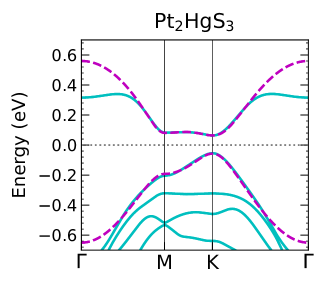
Figure 5 shows band structures for several Pt-based jacutingaite monolayers calculated by DFT-GGA (blue solid lines), as well as the results from the TB model (pink dashed lines). The TB results show very good agreement with the DFT bands within an energy interval of 0.6 eV to 1.0 eV and around the M–K path, which exhibits a quasi-flat dispersion in the conduction bands.


3.2 Honeycomb-Kagome Tight-Binding model performance on jacuntigaite-like materials
A reasonably accurate description of the electronic structure of the jacutingaite can be realized using an approach based on Maximally Localized Wannier Functions (MLWFs) [29]. The TB Hamiltonian obtained from the construction of MLWFs naturally involves a very large number of hopping parameters. For a structure such as that of jacutingaite, within the MLWFs formalism the number of hoppings terms is of the order of thousands. Thus, in order to study finite nanostructures and electronic transport properties, where a large real-space lattice is often required, the computational cost becomes very high. The model proposed in the present work is a TB Hamiltonian with an interaction radius reaching up to the -NNN distance, and provides an accurate low-energy description with only twelve hopping parameters.
From the proposed model, and based on the band structures obtained via DFT, the twelve hopping parameters were defined for each monolayer structure and arranged in the Table 2, 3 and 4, as shown in the Figure 3 (a), (b) and (c), respectively, and for each term of the Equation 1.
-
Pt Pt2ZnS3 -0.012 -0.359 0.024 0.025 Pt2ZnSe3 0.029 -0.406 0.024 0.032 Pt2ZnTe3 0.235 -0.376 -0.043 0.022 Pt2CdS3 0.489 -0.420 0.014 0.021 Pt2CdSe3 0.023 -0.308 0.036 0.019 Pt2CdTe3 0.174 -0.362 0.009 0.012 Pt2HgS3 0.019 -0.217 0.003 0.017 Pt2HgSe3 -0.039 -0.269 0.032 0.024
-
Pt Pt2ZnS3 4.387 0.398 -1.586 0.045 Pt2ZnSe3 4.548 0.428 -1.635 0.034 Pt2ZnTe3 5.291 0.444 -1.957 0.028 Pt2CdS3 4.100 1.296 -0.375 0.031 Pt2CdSe3 5.810 0.716 -1.915 0.344 Pt2CdTe3 7.502 1.455 -1.820 0.543 Pt2HgS3 8.487 1.850 -1.870 0.680 Pt2HgSe3 10.009 0.986 -3.400 0.342
-
Pt Pt2ZnS3 -0.145 -0.020 0.019 0.005 Pt2ZnSe3 -0.188 -0.029 0.022 0.012 Pt2ZnTe3 -0.214 -0.054 0.002 -0.008 Pt2CdS3 -0.398 0.202 0.035 0.012 Pt2CdSe3 -0.199 -0.020 -0.407 0.014 Pt2CdTe3 -0.322 -0.006 -0.370 0.023 Pt2HgS3 -0.184 -0.074 0.379 0.000 Pt2HgSe3 -0.256 -0.068 0.037 0.000
The hopping terms in Table 2 are relatively similar for the different Pt-based jacutingaites, except for the , which is a consequence of the more dispersive valence band of Pt2ZnTe3 as a way of compensating the SOC contribution from Te. The real NNN hopping terms are comparable to the SOC terms, which highlights its importance. In fact, if these terms are neglected, the results become qualitatively different from those obtained from first principles calculations. The negative value of in Table 4 is due to a greater energy difference between M and K(K′) points, being in the conduction band compared to Pt2ZnSe3.
For Pt2CdSe3, Pt2CdTe3, Pt2HgS3 and Pt2HgSe3 the and is about an order of magnitude larger than , due to a stronger hydridization between the orbitals 5D5/2 and S1/2 for these monolayers.
In systems with strong SOC such as jacutingaite-like materials, the quantum numbers are strongly entangled and accurately describe the complexity of the electronic states of these materials. In this work, we are not considering time reversal symmetry breaking, therefore, we do not evidence the .
In Figure 5 we show a comparison between the band structures for each Pt-based jacutingaite monolayer calculated by DFT-GGA and that obtained from the TB model described in the previous section. The TB model for interpenetrating honeycomb and kagome lattices shows good agreement with the DFT-GGA results and is quite accurate along the K(K′)–M direction. We emphasize that this level of accuracy is missing in previous studies, where simpler TB Hamiltonians based on the Kane-Mele model were employed.
It is worth pointing out that quasi-flat bands are not seen in the Kane-Mele model and the states along K(K′)–M present prominent features of the kagome lattice band, as illustrated in Figure 6 for the Pt2HgSe3. The same qualitative behavior is observed for the other considered materials.

The term, which couples the honeycomb and kagome sub-lattices, as given by Equation 9, is responsible for the characteristic shape of the conduction band of jacutingaite, specifically the band flattening along M–K(K′) direction. In Figure 7 one can visualize, for the case of Pt2HgSe3, the energy dispersion both with and without the inclusion of such term in Equation 1. The relevance of considering this coupling when dealing with Pt-based jacutingaite using tight-binding models thus becomes evident.

For Pt-based jacutingaites monolayers, in the absence of SOC, a calculation of the hybrid Wannier center (HWC) from the present TB model, one can observe that they are non-topological systems (see SM, Figure 2 [53]). The SOC thus opens the topological energy gap and that information is also captured by this model (see SM, Figure 3 [53]).
3.3 Jacuntigaite nanoribbons
The calculation of topological invariants allows determining the topological character of a material based on its bulk structure [54], which is very useful for DFT simulation of crystalline systems. Another approach is to explore topological properties in materials is to consider finite size systems and investigate their edge or surface states. The combination of DFT simulations with the second strategy often implies high computational cost, which can be avoided by the use of a DFT derived TB model.
Edge states in topological 2D systems are topologically protected and robust against local perturbations [13, 15]. In case of Pt-based jacutingaite monolayers, which are QSH semiconductors, the edge states are protected by time-reversal symmetry and against backscattering processes, presenting robustness against non-magnetic perturbations [24, 29]. Understanding and manipulating these edge states not only defines the stability of materials, but also diversifies the possibilities for technological applications [20, 22, 45, 46, 47, 55].
We consider Pt-based jacutingaites nanoribbons with symmetric and asymmetric opposite edges. Figure 8 (a) and (b) shows nanoribbons with symmetric armchair and zigzag opposite edges. There is a pair of topological states of opposite spin at each edge connecting the valence and conduction bulk states, as we can visualize in their respective band structure in Figure 8. There are no significant differences in the edge states considering a symmetric or asymmetric configuration of the edge for all cases of Pt-based jacutingaites. The edges have the same geometry, with just a difference in translation in relation to each other and there are no overlap significant between edge states to change its energy dispersion. Since a nanoribbon is wide enough for the interaction between the edges not to destroy the topological character, the topological edge states are characterized predominantly by SOC.

The inclusion of NNN hopping terms can lead to the emergence of edge states, which has been a focus of recent studies [56]. The presence of these states, however, depends on the edge geometry, presence of defects, vacancies and external perturbations. In Figure 8 (a) it is possible to observe the existence of edge states within the energy spectrum of the conduction bands. These states emerge as a consequence of the mapping of asymmetric interactions (Figure 3 (b) and (c)).
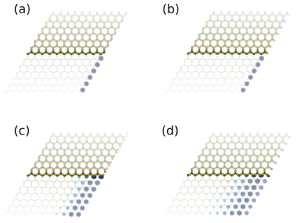
Two Pt2HgSe3 nanoribbons with non-symmetric edges are represented in Figure 9 (a) and (b). For the case Pt2HgSe3 nanoribbon represents in Figure 9 (a) there is a small energy shift and a large momentum shift between the topological states of opposite edges, as shown in Figure 9 (c). For the case of the nanoribbon represents in Figure 9 (b) there is only a small energy shift between the topological states of opposite edges (see Figure 9 (d)). For other Pt-based jacutingaite nanoribbons see SM, Figure 4 and 5.


Depending on the geometric configuration of the edges, the topological edge states can be highly localized at the edges or be more delocalized. In Figure 10, there is a representation of the proportional penetration length of the edge states for Pt2HgSe3 nanoribbons with some possible terminations. For the configurations represented in Figure 10 (a) and (b), the states tend to be often localized, confined to a distance of up to , for both cases, with the value of given in Table 1. For the configurations illustrated in Figure 10 (c) and (d), the edge states tend to be significantly more delocalized, with a penetration length of up to 7 and 11, respectively. A nanoribbon of width 85 was considered for these terminations.
These results show that the corresponding dispersion bands and penetration length of the edge states to the topological edge states of Pt-based jacutingaite finite nanostructures are sensitive to the geometry of the edge. Additionally, these results demonstrate that the TB model can go beyond the computational limitations associated with DFT computational costs. The presented approach opens an avenue to explore large-scale structures in a computationally resource-efficient approach.
4 Conclusion
In this study, we have successfully developed a comprehensive TB model for Pt-based jacutingaite monolayers, meticulously capturing both the conduction and valence band dispersions near the SOC energy gaps. Our model uniquely integrates the linear dispersion characteristics from the K(K′)– points and the downward band from K(K′) to M, significantly enhancing accuracy by incorporating Pt 3e elements. These elements, in conjunction with the metals, form an intricate lattice that is a hybrid of honeycomb and kagome sub-lattices, further enriched by real next-nearest-neighbor (NNN) hopping terms. Considering this model, we were able to reproduce the quasi-flat bands, not seen in the Kane-Mele model, and the states along K(K′)–M, which present prominent features of the kagome lattice band.
The implications of our model are profound, offering a new lens for analysing of the system to obtain more reliable TB Hamiltonians. Our TB model, by accurately describing low-energy regions, enables an in-depth exploration properties of mesoscopic systems, as demonstrated by our analysis of various nanoribbon systems and its topological properties. Furthermore, experimental techniques have been used to explore the robustness of topological states under real conditions. Advances in scanning tunneling microscopy techniques can detect the simultaneity of bulk gaps and metallic edge states [24, 57, 30]. The observation of hybridization effects is enable by high-resolution angle-resolved photoemission measurements at different photon energies [28, 58, 30]. Both the techniques have already been employed in the studies of the Pt2HgSe3, to demonstrate the dual-topological nature in its bulk form [28] and the existence and robustness of QSH states in its 2D form [24]. Theoretical models help in the interpretation and understanding of experimental results, and our model is very promising in playing this role in the future experimental study of Pt-based jacuntigaites.
The potential applications of this model are vast. Our findings contribute not only to a deeper understanding of Pt-based jacutingaite monolayers but also pave the way for future research in this exciting field. Further studies could explore the applicability of our model to other 2D materials or more complicated systems, building on the materials studied in this paper, potentially uncovering new phenomena and guiding the design of next-generation electronic devices.
Acknowledgment
We acknowledge prof. Cristiane Morais Smith, from the Institute of Theoretical Physics at Utrecht University, for the insightful discussions that inspired this work.
This work was financially supported by the Brazilian Council for Research (CNPq) Grants 310422/2019-1
References
References
- [1] Novoselov K S, Geim A K, Morozov S V, Jiang D e, Zhang Y, Dubonos S V, Grigorieva I V and Firsov A A 2004 science 306 666–669
- [2] Katsnelson M I 2007 Graphene: carbon in two dimensions vol 10 (Elsevier)
- [3] Neto A C, Guinea F, Peres N M, Novoselov K S and Geim A K 2009 Reviews of modern physics 81 109
- [4] Dong L X and Chen Q 2010 Frontiers of Materials Science in China 4 45–51
- [5] Bhimanapati G R, Lin Z, Meunier V, Jung Y, Cha J, Das S, Xiao D, Son Y, Strano M S, Cooper V R et al. 2015 ACS nano 9 11509–11539
- [6] Ares P and Novoselov K S 2022 Nano Materials Science 4 3–9
- [7] Xu M, Liang T, Shi M and Chen H 2013 Chemical reviews 113 3766–3798
- [8] Balendhran S, Walia S, Nili H, Sriram S and Bhaskaran M 2015 small 11 640–652
- [9] Gupta A, Sakthivel T and Seal S 2015 Progress in Materials Science 73 44–126
- [10] Gao L 2017 Small 13 1603994
- [11] Guo B, Xiao Q l, Wang S h and Zhang H 2019 Laser & Photonics Reviews 13 1800327
- [12] Glavin N R, Rao R, Varshney V, Bianco E, Apte A, Roy A, Ringe E and Ajayan P M 2020 Advanced Materials 32 1904302
- [13] Hasan M Z and Kane C L 2010 Reviews of modern physics 82 3045
- [14] Isaeva A, Rasche B and Ruck M 2013 Physica status solidi (RRL)–Rapid Research Letters 7 39–49
- [15] Bansil A, Lin H and Das T 2016 Reviews of Modern Physics 88 021004
- [16] Olsen T, Andersen E, Okugawa T, Torelli D, Deilmann T and Thygesen K S 2019 Physical Review Materials 3 024005
- [17] Marrazzo A, Gibertini M, Campi D, Mounet N and Marzari N 2019 Nano letters 19 8431–8440
- [18] Cayssol J and Fuchs J N 2021 Journal of Physics: Materials 4 034007
- [19] Kong D and Cui Y 2011 Nature Chemistry 3 845–849
- [20] Bhardwaj V and Chatterjee R 2020 Resonance 25 431–441
- [21] Kane C L and Mele E J 2005 Physical review letters 95 146802
- [22] Bernevig B A, Hughes T L and Zhang S C 2006 science 314 1757–1761
- [23] Knez I, Du R R and Sullivan G 2011 Phys. Rev. Lett. 107(13) 136603
- [24] Kandrai K, Vancsó P, Kukucska G, Koltai J, Baranka G, Hoffmann Á, Pekker Á, Kamarás K, Horváth Z E, Vymazalová A et al. 2020 Nano letters 20 5207–5213
- [25] Cabral A, Galbiatti H, Kwitko-Ribeiro R and Lehmann B 2008 Terra Nova 20 32–37
- [26] Vymazalová A, Laufek F, Drábek M, Cabral A R, Haloda J, Sidorinová T, Lehmann B, Galbiatti H F and Drahokoupil J 2012 The Canadian Mineralogist 50 431–440
- [27] Facio J I, Das S K, Zhang Y, Koepernik K, van den Brink J and Fulga I C 2019 Physical Review Materials 3 074202
- [28] Cucchi I, Marrazzo A, Cappelli E, Riccò S, Bruno F, Lisi S, Hoesch M, Kim T, Cacho C, Besnard C et al. 2020 Physical review letters 124 106402
- [29] Marrazzo A, Gibertini M, Campi D, Mounet N and Marzari N 2018 Physical review letters 120 117701
- [30] Weber B, Fuhrer M S, Sheng X L, Yang S A, Thomale R, Shamim S, Molenkamp L W, Cobden D, Pesin D, Zandvliet H J et al. 2024 Journal of Physics: Materials 7 022501
- [31] de Lima F C, Miwa R and Fazzio A 2020 Physical Review B 102 235153
- [32] Hohenberg P and Kohn W 1964 Physical review 136 B864
- [33] Kohn W and Sham L J 1965 Physical review 140 A1133
- [34] Giannozzi P, Baroni S, Bonini N, Calandra M, Car R, Cavazzoni C, Ceresoli D, Chiarotti G L, Cococcioni M, Dabo I et al. 2009 Journal of physics: Condensed matter 21 395502
- [35] Giannozzi P, Andreussi O, Brumme T, Bunau O, Nardelli M B, Calandra M, Car R, Cavazzoni C, Ceresoli D, Cococcioni M et al. 2017 Journal of physics: Condensed matter 29 465901
- [36] Sohier T, Calandra M and Mauri F 2017 Physical Review B 96 075448
- [37] Perdew J P, Burke K and Ernzerhof M 1996 Physical review letters 77 3865
- [38] Hamann D 2013 Physical Review B 88 085117
- [39] van Setten M J, Giantomassi M, Bousquet E, Verstraete M J, Hamann D R, Gonze X and Rignanese G M 2018 Computer Physics Communications 226 39–54
- [40] Fletcher R 1987 Practical Methods of Optimization (New York: Wiley)
- [41] Billeter S R, Turner A J and Thiel W 2000 Physical Chemistry Chemical Physics 2 2177–2186
- [42] Billeter S R, Curioni A and Andreoni W 2003 Computational materials science 27 437–445
- [43] Yusufaly T, Vanderbilt D and Coh S 2022 URL http:physics.rutgers.edupythtb
- [44] Tight-binding model of Pt-based jacutingaites, Zenodo, 2024, https://doi.org/10.5281/zenodo.13830889
- [45] Weeks C, Hu J, Alicea J, Franz M and Wu R 2011 Physical Review X 1 021001
- [46] Beugeling W, Everts J C and Smith C M 2012 Physical Review B 86 195129
- [47] Bafekry A, Obeid M, Nguyen C V, Ghergherehchi M and Tagani M B 2020 Journal of Materials Chemistry A 8 13248–13260
- [48] Mauro D, Henck H, Gibertini M, Filippone M, Giannini E, Gutierrez-Lezama I and Morpurgo A F 2020 2D Materials 7 025042
- [49] Luo F, Hao X, Jia Y, Yao J, Meng Q, Zhai S, Wu J, Dou W and Zhou M 2021 Nanoscale 13 2527–2533
- [50] Rehman M U, Qiao Z and Wang J 2022 Physical Review B 105 165417
- [51] Zhu X, Chen Y, Liu Z, Han Y and Qiao Z 2023 Frontiers of Physics 18 23302
- [52] de Lima F C, Focassio B, Miwa R H and Fazzio A 2023 2D Materials 10 035001
- [53] 2024 Supplementary material
- [54] Vanderbilt D 2018 Berry phases in electronic structure theory (Cambridge University Press)
- [55] Rehman M U, Kiani M and Wang J 2022 Physical Review B 105 195439
- [56] Downing C, Martín-Moreno L and Fox O 2024 New Journal of Physics 26 073014
- [57] Yin J X, Pan S H and Zahid Hasan M 2021 Nature Reviews Physics 3 249–263
- [58] Lv B, Qian T and Ding H 2019 Nature Reviews Physics 1 609–626