Theory of the Strain Engineering of Graphene Nanoconstrictions
Abstract
Strain engineering is one of the key technologies for using graphene as an electronic device: the strain-induced pseudo-gauge field reflects Dirac electrons, thus opening the so-called conduction gap. Since strain accumulates in constrictions, graphene nanoconstrictions can be a good platform for this technology. On the other hand, in the graphene nanoconstrictions, Fabry-Pérot type quantum interference dominates the electrical conduction at low bias voltages. We argue that these two effects have different strain dependence; the pseudo-gauge field contribution is symmetric with respect to positive (tensile) and negative (compressive) strain, whereas the quantum interference is antisymmetric. As a result, a peculiar strain dependence of the conductance appears even at room temperatures.
Graphene has been attracting attention as a base for future electronic devices, such as the field-effect transistors (FETs)[1, 2]. In device application, controlling electrical conduction is a critical challenge, and strain engineering is one of the promising solutions[3, 4, 5, 6, 7]. This technique is based on the feature that strain acts as a pseudo-gauge field (magnetic field), reflecting Dirac electrons in graphene. Various attempts to introduce strain into graphene have been made so far [8, 9, 10, 11, 12, 13, 14, 15, 16] and it is notable that graphene can tolerate strain up to 20%[8]. This shows the great potential of strain engineering in graphene. In this Letter, we investigate strain engineering in graphene nanoconstrictions. Since strain is known to accumulate in the constrictions[17, 18], graphene nanoconstrictions can be a promising platform for strain engineering.
The nanoconstrictions are also interesting because they clearly show the quantum interference of the Dirac electrons[19]. Especially, Fabry-Pérot type interference is studied theoretically [20, 21, 22, 23] and experimentally [24, 25]. How quantum interference affects strain engineering is an interesting question.
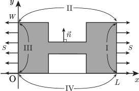
We study the effects of strain on the electrical conduction in graphene nanoconstrictions. The geometry is shown in Fig. 1. The graphene nanoconstriction is made of a single layer graphene and a uniform stress is applied parallel to the lengthwise direction of the wire. We consider both positive (tensile) and negative (compressive) stress for theoretical clarity, although the latter is difficult to realize experimentally in the present geometry. We start from the tight binding model of graphene, whose Hamiltonian is given by
| (1) |
where is the annihilation operator of an electron at the -th site with spin . We limit the electron hopping to the nearest neighbor sites . The hopping matrix element between the -th and -th site is denoted by , which is determined by taking into account the elastic deformation of the lattice due to stress.
First, we determine the strain distribution in the sample. We assume that graphene is an isotropic elastic media. Then, the stress tensor is expressed in terms of the stress function as
| (2) |
and obeys the biharmonic equation with being Laplacian[17, 18]. The strain tensor () is defined using displacement as
| (3) |
and is related to the stress tensor by
| (4) |
where and are Young modulus and Poisson ratio, respectively. The boundary conditions which satisfies are derived from the force balance equations at the boundaries. Let be the unit vector normal to the boundary pointing outward as shown in Fig. 1, we set on the boundaries II and IV, and () on the boundary I (III). These are satisfied by setting as follows,
| (5) |
where is the value on the boundary II (IV). By discretizing the biharmonic equation, we solve numerically. Thereby we find the distribution of strain in the sample.
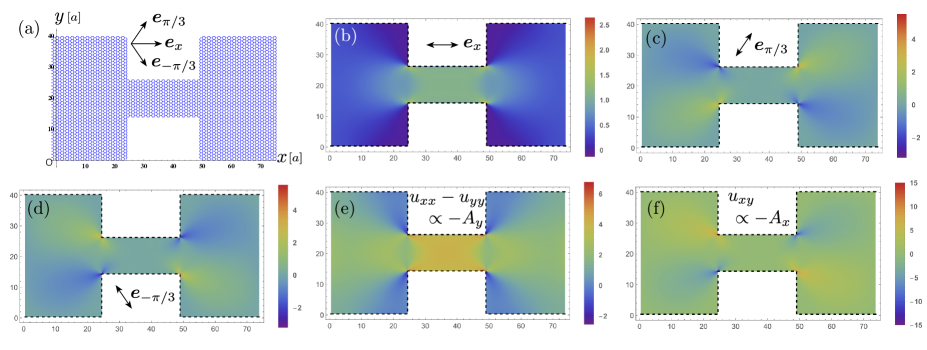
The result corresponding to the stress is depicted in Fig. 2. We can obtain the solution for by multiplying a factor to because the equation that satisfies is linear. In Fig. 2(a), we have shown the lattice and three unit vectors , and , corresponding to three directions of the atomic bonds. Here, the wire is aligned in the armchair direction so that the strain engineering works most efficiently[3]. The change in the bond length between the -th and -th site is given, using strain tensor , as , where is the position of the -th site, , is the carbon-carbon distance (0.142 nm), and is a numerical factor [26]. Figures 2(b), (c), and (d) show the change rates of the bond length parallel to , , and , respectively. We see from Fig. 2(b) that the bonds are significantly stretched in the constriction region as expected. From Figs. 2(c) and (d), we see that the bonds at the corners are stretched (shrunk) depending on their direction.
In Figs. 2(e) and (f) we have shown the profile of the pseudo-gauge field [26, 27, 4]. In our notation, and , where is a numerical factor, and is the lattice constant. We see that , which is supposed to suppress the conduction along the wire, is largely generated at the constriction[3]. We note that the pseudo-gauge field is not uniform in our system, and we also have as well as . Their effects on the electrical conductance may be non-trivial.
Base on the above results, we define the hopping matrix elements of the Hamiltonian as
| (6) |
where is the hopping integral without distortion [26, 28]. Here we adopted exponential form so that it remains positive even for a large distortion.
We have calculated the conductance of the wire at under strain, in terms of recursive Green function method[29], where is the energy of the incident electron or the bias voltage divided by the electron charge . At a finite temperature , the conductance is calculated from
| (7) |
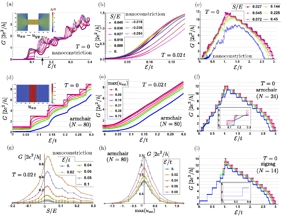
The wider and narrower part of the nanoconstriction are assumed to be and armchair nanoribbon, respectively[30, 31]. For comparison, we have also calculated the conductance of and armchair nanoribbons and zigzag nanoribbon, with an ideal uniaxial strain applied parallel to the lengthwise direction of the ribbon as depicted in the inset of Fig. 3(d).
Figures 3(a) and (c) show the dependence of the conductance of the nanoconstriction at , and (b) is that at (room temperature); (a) and (b) are focused on the region near whereas (c) shows the full band width. The legend is common between (a) and (b). We see from Figs. 3(a) and (c) that shows many peaks and jumps at low temperatures. We attribute this behavior to the Fabry-Pérot type quantum interference of the Dirac electrons at the constriction[22], although the peaks in our results are much less periodic or sharp than those in a well-shaped Fabry-Pérot interferometer[32]. In a nanoconstriction made of a wire of length , the Fabry-Pérot resonance occurs when the characteristic wavelength satisfies , with being an integer. In the present case, is the wavelength of the Bloch electron in the wire, and we may set with being the Fermi velocity. If we put the effective wire length as , the resonant energy becomes . This shows a rough match with the peak structure in Fig. 3(a).
In Fig. 3(a), a peak located at (indicated by an arrow) shows a systematic shift to low bias side as the strain increases. The strain, which changes the hopping integral , may shift the peak positions. Let us estimate its amount. From Fig. 2(b), the change rate in the bond length at the constriction is for and, then, for , is 1.52.0%. According to Eq. (6), the decrease in is estimated to be 3.04.0%. Then, the peak position shift is expected to be the same amount, which roughly agrees with the peak shift observed in Fig. 3(a). For the understanding of the full properties, including the peak height and so on, we need more detailed analysis, however.
The above features are in stark contrast to the case of armchair nanoribbons shown in Figs. 3(d) and (f), where the conductance steps are uniformly and monotonically smoothen by increasing strain.
In Fig. 3(b), we see that, at a finite temperature, the conductance of the nanoconstriction shows no peaks or jumps, unlike case. However, it exhibits an irregular strain dependence compared to the armchair nanoribbon (Fig. 3(e)). In Fig. 3(g), we have plotted for several values of as a function of . We see that the maximum of the conductance is located at a positive (tensile) strain side. Then, applying the stress at first increases conductance contrary to the strain engineering theory[3]. In contrast, the conductance of armchair nanoribbon (Fig. 3(h)) has the maximum at the origin and is symmetric with respect to positive and negative . The reason for this discrepancy could be attributed to the quantum interference effect which we have seen above for the case. That is, the tensile stress pushes the peaks of quantum interference down to low energy side, and as a result, the low-bias conductance increases. This effect is antisymmetric with respect to in contrast to the pseudo-gauge field effect of strain engineering, which is symmetric[33]. In the present study, experimentally accessible region ( % or ) covers only a narrow range of Figs. 3(g) and (h). We consider that our results may become easier to access by making the system size larger since the pseudo-magnetic field effect becomes more apparent.
Figures 3(c), (f) and (i) show the conductance of the nanoconstriction, armchair nanoribbon and zigzag nanoribbon, respectively. In all the plots the strain effects are pronounced above . However, we see that the behaviors near are different; (c) shows resonance like peaks as we have seen in Fig. 3(a), (f) shows a monotonic decrease as strain is enhanced and (i) shows no dependence on the strain at all. The behavior of (f) and (i) are consistent with Ref. \citenPereira:2009cha.
From the above findings, we argue that the effects of strain on the conductance in nanoconstrictions are dominated by the two effects: 1) the pseudo-gauge field effect, which suppresses the conductance with stress-even dependence, and 2) the Fabry-Pérot type quantum interference effect, which enables resonant transport through the constriction, thus adding stress-odd contribution.
Recently, several attempts to tune the stress on nanoconductors have been made, which enables highly controllable strain devices [34, 35]. We hope that our results may be useful for future experiments.
In conclusion, we have studied the strain-dependent conductance of the graphene nanoconstrictions and found that interplay between pseudo-gauge field effect, which is expected from strain engineering theory, and Fabry-Pérot type quantum interference effect, which is characteristic to nanoconstrictions, induces peculiar strain dependence of the electric conductance. Our results may be experimentally accessible.
This work was supported by JSPS KAKENHI Grant Numbers 24540392 and 15K04619.
References
- [1] K. S. Novoselov, A. K. Geim, S. V. Morozov, D. Jiang, Y. Zhang, S. V. Dubonos, I. V. Grigorieva, and A. A. Firsov: Science 306, 666 (2004).
- [2] K. S. Novoselov, A. K. Geim, S. V. Morozov, D. Jiang, M. I. Katsnelson, I. V. Grigorieva, S. V. Dubonos, and A. A. Firsov: Nature 438, 197 (2005).
- [3] V. M. Pereira and A. H. Castro Neto: Phys. Rev. Lett. 103, 046801 (2009).
- [4] F. Guinea, M. I. Katsnelson, and A. K. Geim: Nat. Phys. 6, 30 (2010).
- [5] F. Guinea, A. K. Geim, M. I. Katsnelson, and K. S. Novoselov: Phys. Rev. B 81, 035408 (2010).
- [6] F. Guinea: Solid State Commun. 152, 1437 (2012).
- [7] D. A. Bahamon and V. M. Pereira: Phys. Rev. B 88, 195416 (2013).
- [8] C. Lee, X. Wei, J. W. Kysar, and J. Hone: Science 321, 385 (2008).
- [9] N. Levy, S. A. Burke, K. L. Meaker, M. Panlasigui, A. Zettl, F. Guinea, A. H. C. Neto, and M. F. Crommie: Science 329, 544 (2010).
- [10] H. Tomori, A. Kanda, H. Goto, Y. Otsuka, K. Tsukagoshi, S. Moriyama, E. Watanabe, and D. Tsuya: Appl. Phys. Express 4, 075102 (2011).
- [11] A. Reserbat-Plantey, D. Kalita, Z. Han, L. Ferlazzo, S. Autier-Laurent, K. Komatsu, C. Li, R. Weil, A. Ralko, L. Marty, S. Guéron, N. Bendiab, H. Bouchiat, and V. Bouchiat: Nano Lett. 14, 5044 (2014).
- [12] J. Choi, H. J. Kim, M. C. Wang, J. Leem, W. P. King, and S. Nam: Nano Lett. 15, 4525 (2015).
- [13] Y. Jiang, J. Mao, J. Duan, X. Lai, K. Watanabe, T. Taniguchi, and E. Y. Andrei: Nano Lett. 17, 2839 (2017).
- [14] B. Pacakova, T. Verhagen, M. Bousa, U. Hübner, J. Vejpravova, M. Kalbac, and O. Frank: Sci. Rep. 7, 10003 (2017).
- [15] Y. Zhang, M. Heiranian, B. Janicek, Z. Budrikis, S. Zapperi, P. Y. Huang, H. T. Johnson, N. R. Aluru, J. W. Lyding, and N. Mason: Nano Lett. 18, 2098 (2018).
- [16] C. C. Hsu, M. L. Teague, J. Q. Wang, and N.-C. Yeh: Sci. Adv. 6, eaat9488 (2020) .
- [17] S. Timoshenko, J. N. Goodier, and J. N. Goodier: Theory of Elasticity (McGraw-Hill, 1951).
- [18] L. D. Landau, E. M. Lifshitz, A. M. Kosevich, J. B. Sykes, Pitaevskii, L.P., and W. H. Reid: Theory of Elasticity (Elsevier Science, 1986).
- [19] F. Muñoz-Rojas, D. Jacob, J. Fernández-Rossier, and J. J. Palacios: Phys. Rev. B 74, 195417 (2006).
- [20] A. V. Shytov, M. S. Rudner, and L. S. Levitov: Phys. Rev. Lett. 101, 156804 (2008).
- [21] M. Ramezani Masir, P. Vasilopoulos, and F. M. Peeters: Phys. Rev. B 82, 115417 (2010).
- [22] P. Darancet, V. Olevano, and D. Mayou: Phys. Rev. Lett. 102, 136803 (2009).
- [23] M. Yang and J. Wang: New J. Phys. 16, 113060 (2014).
- [24] M. T. Allen, O. Shtanko, I. C. Fulga, J. I. J. Wang, D. Nurgaliev, K. Watanabe, T. Taniguchi, A. R. Akhmerov, P. Jarillo-Herrero, L. S. Levitov, and A. Yacoby: Nano Lett. 17, 7380 (2017).
- [25] N. F. Ahmad, K. Komatsu, T. Iwasaki, K. Watanabe, T. Taniguchi, H. Mizuta, Y. Wakayama, A. M. Hashim, Y. Morita, S. Moriyama, and S. Nakaharai: Sci. Rep. 9, 3031 (2019).
- [26] H. Suzuura and T. Ando: Phys. Rev. B 65, 235412 (2002).
- [27] J. L. Mañes: Phys. Rev. B 76, 045430 (2007).
- [28] A. H. Castro Neto, N. M. R. Peres, K. S. Novoselov, and A. K. Geim: Rev. Mod. Phys. 81, 109 (2009).
- [29] T. Ando: Phys. Rev. B 44, 8017 (1991).
- [30] M. Fujita, K. Wakabayashi, K. Nakada, and K. Kusakabe: J. Phys. Soc. Jpn. 65, 1920 (1996).
- [31] For armchair nano-ribbons, is the number of dimers per unit cell, and for zigzag nano-ribbons, is the number of zigzag chains[30]. Actual width of these wires are almost the same.
- [32] According to the Ref. \citenDarancet:2009dw, the condition for well-defined Fabry-Pérot resonance is . In our case, this yields to . Therefore the resonance in our system is not perfect.
- [33] Here we note that the conductance depends on the constriction’s detailed shape and the conductance maximum can be located in the negative region in other shapes. This is probably due to the complicated interference effects and will be discussed elsewhere.
- [34] C. Androulidakis, E. N. Koukaras, J. Parthenios, G. Kalosakas, K. Papagelis, and C. Galiotis: Sci. Rep. 5, 18219 (2015).
- [35] S. Caneva, P. Gehring, V. M. García-Suárez, A. García-Fuente, D. Stefani, I. J. Olavarria-Contreras, J. Ferrer, C. Dekker, and H. S. J. van der Zant: Nat. Nanotechnol. 13, 1126 (2018).