Suppressing quantum effects by optically-driven nonequilibrium phonons
Abstract
Optically-generated nonequilibrium phonon-distribution is used for exploring the origin of a nonlocal adiabatic response in an interacting Anderson insulator. Exposing the system to weak infrared radiation is shown to effectively suppress a long-range effect observed in field-effect experiments while producing little heating and barely changing the system conductance. These effects are shown to be consistent with the quantum nature of the effect and therefore are peculiar to disordered systems that are quantum-coherent.
The wavefunctions of Anderson insulators are commonly visioned as decaying exponentially in space away from their localization center. Localized wavefunctions with more complicated envelopes, extending over scales longer than the localization length, are exponentially rare. Associated with this view is the premise that correlations between spatially-separated states may be neglected. In case of static disorder, this is a plausible approach for most realistic situations. When the system is exposed to a time-dependent potentials however, correlations between wavefunctions of distant sites may appear that could significantly modify transport properties of the system.
In this spirit, Khemani et al 1 proposed that slowly varying the potential applied to a site localized at would produce a disturbance in other localized-sites that are many ’s apart from . The local potential-change V must however be slow enough such that during t the process remains adiabatic. This condition leads to a spatial range influenced by the local potential-manipulation, r, 1 :
| (1) |
where W is the disorder responsible for the localization, V/t is the rate of the local potential change. In the presence of a finite phase-coherent time , the range is limited to Lϕ ·(W/) 1 or by r, whichever is smaller. Accordingly, the cutoff length at high temperature (or slow V/t) would be set by Lϕ, which due to lack of theory, has to be estimated on the basis of independent measurement. Note that Lϕ depends on the coherence time but not on the diffusion constant, unlike the situation in weak-localization. Also, the prefactor in both Eq.1 and Lϕ are yet to be determined by a proper theoretical model.
This quantum-mechanical effect was recently considered as a possible explanation for a long-range influence of varying the local potential in field-effect measurements performed on electron-glasses 2 . In the experiment, the surface potential at the bottom of a sample, controlled by a gate, affected its entire thickness of 82nm, 20 times larger than the localization length.
A crucial aspect of this nonlocal mechanism, heretofore untested, is that the rate of potential-change, V/t is a dynamic parameter that controls the range of influence. Sweeping the gate-voltage V as a means of manipulating V/t is a viable technique to keep the process adiabatic but being limited to relatively small frequencies it is not an effective way to test the logarithmic dependence (Eq.1); To reduce the logarithmic factor that is typically 20-30 by a factor of two, V/t has to be increased by 6-8 orders of magnitude. This range of frequencies cannot be implemented with a standard field-effect technique. As an alternative we employ in this work optically-generated nonequilibrium-phonons to modulate the sites potential with THz frequencies. It turns out that even a very weak intensity of this disturbance dramatically suppresses the long-range effect associated with r while the system effective temperature and conductance are barely affected. This technique, which has been used in a number of solid-state projects 3 , is contrasted with another nonequilibrium steady-state (NESS) by measuring the system conductance away from linear-response. The results demonstrate the diversity of outcomes obtainable by subjecting a quantum system to different NESS protocols. In particular, the outcome of a protocol depends on the frequency of the drive, not on its intensity, in similar vein with the photoemission versus thermal-emission phenomenon. It has also bearing on energy-transfer issues of open quantum systems 4 .
Like all quantum effects, the long-range of influence produced by changing the potential locally is ultimately limited by the phase-coherence of the medium. The experimental results of this work confirm that coherence length comparable with what is achievable in diffusive systems at low temperatures are attainable in some systems. Apparently however, this property is less common than seems to be generally recognized.
The samples used in this study were amorphous indium-oxide InO films with low carrier-concentration N(10.1)x10cm. These were configured as MOSFET devices for field-effect measurements 5 .
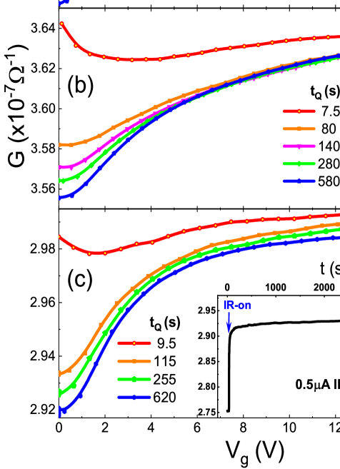
The main results of this study are summarized in the set of measurements presented in Fig.1. These include four experiments performed on a single sample with thickness d=8520nm and relatively high degree of disorder; the Ioffe-Regel parameter k of this sample is 0.04, deep on the insulating side.
Fig.1a, Fig.1b, and Fig.1c show a series of conductance vs. gate-voltage G(V) traces taken at different times t. The time is measured from the moment the system was quenched from a random state and allowed to relax at the measurements temperature T=4.11K. Exciting the system to achieve randomization is accomplished by exposing the sample to an AlGaAs diode generating infrared radiation at a wavelength 0.850.05m. This device was mounted on the sample-stage 12-15mm from the sample surface. This is done, using a computer-controlled Keithley 220, by passing a current of 0.5mA (with forward bias =1.3V) through the diode for 3 seconds.
Shortly after the brief exposure to the IR source is terminated, the G(V,t) traces are recorded. Each trace is taken from V=0 to V=14V with a constant rate of 0.6V/s. Between subsequent scans the sample is kept under V=0 allowing the sample to relax as manifested by a memory-dip (MD) 6 ; 7 growing deeper with time. Figure 1b shows the results of the same protocol as in Fig.1a except that the G(V,t) traces were taken using a non-ohmic source-drain bias. The non-ohmic measurements resulted in higher conductance, and wider and shallower MD (see, Fig.2).
A modified protocol was used to obtain the data shown in Fig.1c. This protocol starts by allowing the sample to reach a steady-state under a weak IR radiation; about one thousandth of the intensity used for completely randomizing the system. Turning on this radiation promptly increases the system conductance that, in this sample, eventually settles at a 6% higher than its equilibrium value as shown in Fig.1c. The rest of the protocol involves the same steps as in Fig.1a, and Fig.1b (the weak IR is kept throughout the duration of this protocol). Note that the G(V,t) curves in Fig.1c become parallel over the range of V where the G(V,t) traces in Fig.1a, and Fig.1b are converging to a common plot.
Between protocols the sample was allowed to recover for at least 24 hours. Each protocol in Fig.1 was repeated twice to ascertain reproducibility.
A simple explanation for the results in Fig.1c is that the charge added by V affects only the part of the sample in the vicinity of the sample-spacer interface while the rest of it is unaffected. In this case the sample is effectively composed of two conductors in parallel; one where the G(V,t) curves are like the pattern exhibited by the sample in Fig.1a, and another for which G(t) just monotonically decreases after being ”quench-cooled”, independent of V. Superimposing these two components reproduces the G(V,t) curves exhibited in Fig.1c.
By contrast, using either, the linear-response or the non-ohmic protocols (Fig.1a and Fig.1b respectively), the converging G(V,t) traces suggest that changing the gate-voltage affects the entire sample volume. This long-range influence, first seen on a thin sample (5nm InO film 6 ) is shown here to extend up to 85nm.
Comparing Fig.1b with Fig.1c and the conditions under which the respective data were taken, one may conclude the following:
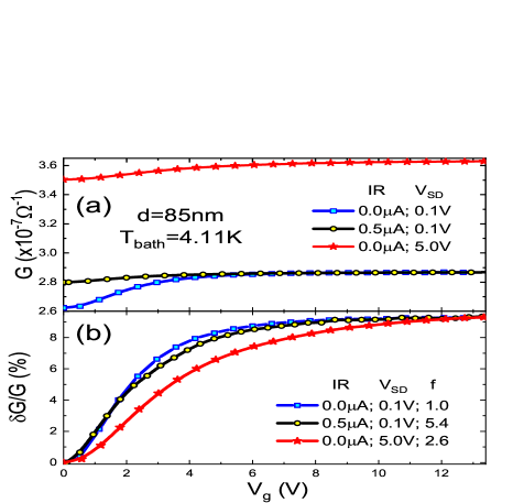
The reason for the suppression of the long range effect by the IR radiation is neither due to a change of the system conductance nor due to heating: Note that heating and conductance-enhancement are much more conspicuous in the V=5V protocol while leaving the long-range effect essentially intact (Fig.1b).
Another feature that clearly marks the V=5V protocol as the ”hotter” state is shown in Fig.2b. It illustrates how the shape of the MD, for the two different NESS protocols, deviates from the MD taken under ohmic-conditions and in the dark. The non-ohmic MD shape is significantly broader than the ohmic curve and it is consistent with the G(V) obtained at elevated temperatures 6 ; 8 . Intriguingly, G(V) taken under the weak-IR, while it is reduced in magnitude by a factor of 5.4 (as compared with just 2.6 for the 5V bias, see Fig.2), its shape deviates from the ”reference” much less than in the non-ohmic case. The latter feature is consistent with the smaller excess energy imparted to the system which is not surprising given the large disparity in the power invested in the system by the different sources; The power associated with V=5V is 20 times larger than that generated by the IR diode. The more pronounced effect of the IR on the MD magnitude, G/G is a result of the different way the energy absorbed from the 5V bias and IR fields is distributed among the system degrees of freedom.
If the change of the sample conductance G under either NESS protocol is related to an excess temperature T by using the G(T) of the sample 9 then T40mK under the weak IR and T300mK for the non-ohmic bias condition. It should be observed that while G(T) is an equilibrium result G is measured under NESS conditions. Therefore, these T’s should be regarded as merely order of magnitude values and will be treated as such in our estimates for r detailed below.
We now show that the results of the experiments described above can be heuristically accounted for by the quantum scenario proposed in 1 and the peculiarity of the nonequilibrium phonon distribution resulting from the weak-IR illumination.
The range of disturbance created by a local change of the potential is limited by either Lϕ or by V/t. Using Eq.1 and Lϕ ·(W/) with W0.4eV, 10s, 5nm, and V/t0.6meV/s 10 yields r L100nm. This agrees with our linear-response results (Fig.1a). The situation changes when the system is exposed to the IR source. This initiates a cascade process 11 : Electrons are excited to high-energy, then relax by phonons emission. The NESS that eventually sets-in (Fig.1c), sustains vibrations at typical phonon frequencies f10s; the energy of optical-phonons in InO is spread over the interval of 350-500cm (0.043-0.062eV) 12 ,. The associated excess energy sustains a potential-amplitude V. The NESS that characterizes the weak-IR protocol involves a flow of energy from the electronic system to the phonons and into the bath. Given the small in-going power involved, the lack of detailed balance may be neglected and it is then plausible to assume that the electronic system is close to equilibrium with the phonons. Then V may be estimated from:
| (2) |
where C is heat-capacity per electron, k is the Boltzmann constant, and T is the Fermi temperature. With T750K, and T40mK noted above, V is of the order of 0.1V giving V·f that is about 10 times larger than the respective value for the linear-response conditions. Inserted in Eq.1 this factor reduces the linear-response value r100nm to r60nm. This means that, under the weak-IR, the range-of-influence becomes smaller than the film thickness consistent with the results shown in Fig.1c.
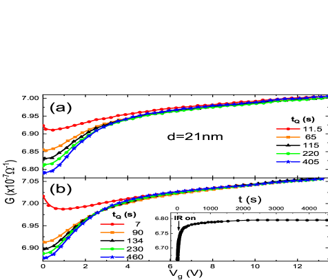
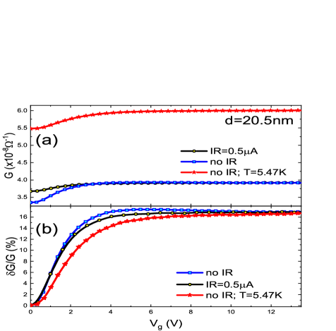
A natural further test of this conjecture, is to apply the same protocol on samples that are thinner than 60nm. Three thin (20nm) InO batches were prepared for this purpose, with the same composition as the 85nm sample, attempting to match all relevant material parameters. Results of these measurements are shown in Fig.3 and Fig.4 for two of the samples, one with resistance smaller and the other with larger resistance than that of the 85nm sample.
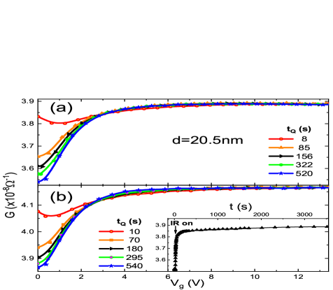
In both samples, the weak-IR decreased the magnitude of the MD, but the G(V,t) plots converged to a common curve suggesting that the reduced range of influence associated with V·f is still larger than the thickness of these samples in accord with the above estimate for r. At the same time, the effect of the weak IR illumination on the 20nm films, as shown in Fig.5, is qualitatively similar to the thick film (Fig.2). Quantitatively however, the reduction of the MD magnitude by the weak-IR is by a factor of 2 as compared with 5.4 found in the 85nm film. The larger effect in the latter case is another aspect of the cause for the non-converging G(V,t) plots: Once r (or Lϕ) becomes smaller than the film thickness, the G due to V is shunted by the conductance of the unaffected top layer, thus further reducing the value of G/G relative to the thin-film case.
To conclude, the set of empirical evidence described in this work support the conjecture that the range of the disturbance caused by varying the gate-voltage may be limited by introducing nonequilibrium phonons. The associated high frequency of the ensuing potential modulation presumably violates the condition of adiabaticity. It is noteworthy that, as long as the modulation amplitude is weak enough, then up to THz frequencies, this limitation still allows for nonlocal influence on a significantly large scale of 50nm. This should make it feasible to observe quantum effects such as the orthogonality catastrophe 1 , which is anticipated to be significant in the Anderson insulating phase 13 . It would also be relevant for observing modifications of ac conductivity in disordered solids 14 over a wide range of frequencies. The pre-requirement for these and other long-scale quantum-effects is that phase-coherence must extend throughout the system to start with. This caveat is rarely mentioned explicitly in theoretical papers but it is far from a trivial issue in reality. Unfortunately, little attention has been given to develop tools for assessing the spatial range of coherence in strongly-disordered insulators, and very few experimental studies were dedicated to look for quantum effects. Anisotropic magnetoconductance has been reported in 2D films 15 and quasi-1D wires 16 of Anderson insulating InO samples consistent with quantum-interference mechanism, and by inference, demonstrating quantum coherence on scales that exceed the localization length of the system. On the other hand, there are systems where these quantum-effects, while clearly observable in the diffusive regime, vanished or became overwhelmed by another mechanism once the system crossed over to the insulating side 17 . It appears that in some materials a dephasing mechanism is turned on in their localized phase, possibly related to the appearance of local magnetic-moments associated with singly-occupied sites 18 . Unless compensated by some mechanism, these are a potential source of dephasing 19 . This fundamental issue is relevant for all aspects of quantum transport and it deserves serious experimental and theoretical elucidation.
Acknowledgements.
Discussions with Oded Agam, and Ady Vaknin are gratefully acknowledged. This research has been supported by a grant No 1030/16 administered by the Israel Academy for Sciences and Humanities.References
- (1) Vedika Khemani, Rahul Nandkishore, and S. L. Sondhi, Nonlocal adiabatic response of a localized system to local manipulations, Nature Physics, 11, 560 (2015).
- (2) Z. Ovadyahu, Long-range influence of manipulating disordered-insulators locally, Phys. Rev. B 101, 094202 (2020).
- (3) J.C.V. Mattos and R.C.C. Leite, Nonequilibrium phonon distribution and electron-phonon coupling in semiconductors, Solid State Com., 12, 465, (1973); M. N. Wybourne and J. K. Wigmore, Spectroscopy of high-frequency phonons, Rep. Prog. Phys. 51, 923 (1988); W. E. Bron, T. Juhasz, and S. Mehta, New Nonequilibrium Phonon State, Phys. Rev. Lett., 63, 3655 (1989); J. B. Hertzberg, O. O. Otelaja, N. J. Yoshida, and R. D. Robinson, Non-equilibrium phonon generation and detection in microstructure devices, Rev. Sci. Instr. 82, 104905 (2011).
- (4) L. D. Alessio, and A. Polkovnikov, Many-body energy localization transition in periodically driven systems. Ann. Phys. 333, 1933 (2013); M. F. Ludovico, F. Battista, F. von Oppen, and L. Arrachea, Phys. Rev. B 93, 075136 (2016); Marìa Florencia Ludovico, Michael Moskalets, David Sánchez, and Liliana Arrachea, Dynamics of energy transport and entropy production in ac-driven quantum electron systems, Phys. Rev. B 94, 035436 (2016).
- (5) See Supplemental Material at [URL will be inserted by publisher] for details of preparation, characterization and fuller measurements techniques.
- (6) A. Vaknin, Z. Ovadyahu, and M. Pollak, Non-Equilibrium Field Effect and Memory in the Electron-Glass, Phys. Rev. B 65, 134208 (2002).
- (7) C. C. Yu, Time-dependent development of the Coulomb gap, Phys. Rev. Lett., 82, 4074 (1999); M. Müller and L. B. Ioffe, Glass Transition and the Coulomb Gap in Electron Glasses, Phys. Rev. Lett. 93, 256403 (2004); Vikas Malik and Deepak Kumar, Formation of the Coulomb gap in a Coulomb glass, Phys. Rev. B 69, 153103 (2004); Eran Lebanon, and Markus Müller, Memory effect in electron glasses: Theoretical analysis via a percolation approach, Phys. Rev. B 72, 174202 (2005); M. Müller and E. Lebanon, History dependence, memory and metastability in electron glasses, J. Phys. IV France, 131, 167 (2005); Y. Meroz, Y. Oreg and Y. Imry, Memory effects in the electron glass, EPL, 105, 37010 (2014).
- (8) See Supplemental Material at [URL will be inserted by publisher] for a pertinent example.
- (9) See Supplemental Material at [URL will be inserted by publisher] for the calibration curve.
- (10) See Supplemental Material at [URL will be inserted by publisher] for determination of these parameters.
- (11) Z. Ovadyahu, Optical excitation of electron glasses, Phys. Rev. B 83, 235126 (2011).
- (12) Z. Ovadyahu, Some finite temperature aspects of the Anderson transition, J. Phys. C 19, 5187 (1986).
- (13) Dong-Ling Deng, J. H. Pixley, Xiaopeng Li, and S. Das Sarma, Exponential orthogonality catastrophe in single-particle and many-body localized systems, Phys. Rev. B 92, 220201(R) (2015). For the distinction between these and the ”traditional” orthogonality-catastrophe treatment see: S. Kettermann, Exponential orthogonality catastrophe at the Anderson metal-insulator transition, Phys. Rev. Lett. 117, 146602 (2016).
- (14) S Gopalakrishnan, M Müller, V Khemani, M Knap, Low-frequency conductivity in many-body localized systems, Phys. Rev. B 92, 104202 (2015); T. Dillon Liu, J. T. Chalker, Vedika Khemani and S. L. Sondhi, Mott, Floquet, and the response of periodically driven Anderson insulators, Phys. Rev. B 98, 214202 (2018).
- (15) Z. Ovadyahu, Anisotropic Magnetoresistance in a Fermi Glass, Phys. Rev. B 33, 6552 (1986); O. Faran and Z. Ovadyahu, Magneto-conductance in the Variable Range Hopping Regime due to a Quantum Interference Mechanism, Phys. Rev. B 38, 5457 (1988).
- (16) Z. Ovadyahu, Quantum coherent effects in Anderson insulators, Waves in Random Media, 9(2), 241 (1999).
- (17) Johannes Reindl, Hanno Volker, Nicholas P. Breznay and Matthias Wuttig, Persistence of spin memory in a crystalline, insulating phase-change material, npj Quantum Materials, 57 (2019).
- (18) E. Yamaguchi, H. Aoki, and H. Kamimura, Intra- and interstate interactions in Anderson localised states, J. Phys. C: Solid State Phys., 12, 4801 (1979); L. Fleishman and P. W. Anderson, Interactions and the Anderson transition, Phys. Rev. B 21, 2366 (1980).
- (19) B. I. Shklovskii, and B. Z. Spivak, Scattering and Interference Effects in Variable Range Hopping Conduction, in: Modern Problems in Condensed Matter Sciences, Edited by Pollak M. and Shklovskii B., Ch. 9 (1991); B. Z. Spivak, Anomalous spin magnetoresistance in the region of variable-range hopping conductivity, Zh. Eksp. Teor. Fiz. 87, 1371 (1984); [Sov. Phys. JETP, 60, 4 (1984)]; K. V. Kavokin, Spin relaxation of localized electrons in n-type semiconductors, Semicond. Sci. Technol. 23, 114009 (2008).