Suppressing Andreev bound state zero bias peaks using a strongly dissipative lead
Abstract
Hybrid semiconductor-superconductor nanowires are predicted to host Majorana zero modes, manifested as zero-bias peaks (ZBPs) in tunneling conductance. ZBPs alone, however, are not sufficient evidence due to the ubiquitous presence of Andreev bound states in the same system. Here, we implement a strongly resistive normal lead in our InAs-Al nanowire devices and show that most of the expected ZBPs, corresponding to zero-energy Andreev bound states, can be suppressed, a phenomenon known as environmental Coulomb blockade. Our result is the first experimental demonstration of this dissipative interaction effect on Andreev bound states and can serve as a possible filter to narrow down ZBP phase diagram in future Majorana searches.
Electron tunneling in a dissipative environment has been widely studied before by probing the transport properties of a single nanoscale tunnel junction with highly resistive source/drain leads [1, 2, 3, 4, 5, 6, 7]. The tunneling electrons interact with the electro-magentic plasmon modes of this ohmic environmental bath, resulting in a suppression of the tunneling current or conductance () at low bias voltage () and temperature (), a phenomenon known as ‘environmental Coulomb blockade’ (ECB) or ‘dynamical Coulomb blockade’. This suppression exhibits a power-law as max, similar to the tunneling behavior in a Luttinger liquid [8], where is the Boltzmann constant, is the ratio between the lead resistance (R) and the quantum resistance (). or defines the dissipation strength. Though no real Luttinger liquid is present in dissipative tunneling, theory [9] has demonstrated a mapping connecting this two physically distinct systems where in both cases the tunneling electron’s charge interacts with a continuum (linear) spectrum of bosonic modes. Later on, replacing the metallic tunnel junction with a semiconductor nanostructure, e.g. a quantum point contact [10, 11] or a quantum dot [12, 13, 14, 15], significantly increases the system’s tunability and enables various quantum phase transitions. For example, in a quantum dot system with a single dot level resonantly coupled to the dissipative source and drain leads with the coupling strength being , both experiment [13] and theory [15] have demonstrated that 1) in the asymmetric coupling regime (), the Coulomb conductance peaks are significantly suppressed as decreases, same to the typical ECB suppression for the single barrier case; 2) in the symmetric coupling regime (), the Coulomb peak’s height will, on the contrary, increase as decreases and finally saturates to the quantized conductance of .
Motivated by this striking contrast between symmetric regime versus asymmetric, theory [16] has proposed that a strongly dissipative lead can be implemented in hybrid semiconductor-superconductor nanowire devices to distinguish signatures of Majorana zero mode (MZMs) [17, 18, 19, 20]. Probing MZMs with a regular normal lead reveals zero-bias peaks (ZBPs) in tunneling conductance. The quantitative behavior of the ZBPs observed in experiments [21, 22, 23, 24, 25, 26], however, does not fully follow the simplest MZM theory’s prediction. For example, the perfect Majorana quantization [27, 28] has not been observed yet. This quantization is enabled by Andreev reflection where the injected electrons and Andreev reflected holes ‘see’ the same barrier twice, similar to the quantum dot case with symmetric resonant tunneling () which leads to perfect transmission and ZBP quantization. On the other hand, the biggest challenge of Majorana hunting comes from the co-existence of Andreev bound states (ABS) in the same device system [29]. These ABS-induced ZBPs, superficially similar to MZM signatures, can easily emerge due to potential inhomogeneity [30, 31, 32, 33] or disorder [34, 35, 36, 37] which is currently unavoidable [38]. The tunneling conductance of these ABS is also mediated by Andreev reflection where the tunnel couplings of the electrons and holes are usually different, similar to the quantum dot case with asymmetric coupling (). As a result, the heights of these ZBPs are generally not quantized. Therefore, a dissipative lead with large enough could suppress the ubiquitous ABS-induced ZBPs (asymmetric coupling) at low , while the quantized ZBPs due to symmetric coupling should still survive as long as the dissipation strength is less than 1/2 [16].
In this paper, we engineer such a dissipative lead in our hybrid InAs-Al devices and demonstrate that strong dissipation can indeed suppress most of ZBPs formed from zero-energy ABSs. The survival of quantized ZBPs, possibly due to MZMs or quasi-MZMs, will be studied in the future. We note that the key idea of this proposal [16] is based on the local features of Majorana resonance. Therefore, it can not distinguish topological MZMs from quasi-MZMs due to fine-tuned smooth potential [31, 39, 40] or disorder [41], which gives two spatially separated MZMs in the topological trivial regime.
Fig. 1a shows a scanning electron microscope (SEM) image of the device (Device A). The Cr/Au film (red) was made thin and resistive, serving as an ohmic dissipative environment (referred as ‘dissipative resistor’ for the rest). This dissipative resistor is connected to the InAs-Al hybrid nanowire through the Ti/Au contacting lead (yellow). The resistance of the contacts is negligible due to its large thickness ( 75 nm). The resistance of the dissipative resistor is estimated to be 5.46 k based on an independent calibration of a four-terminal Cr/Au film fabricated together with this device (see Sfig. 1 for details). A total bias voltage is applied to the left most yellow lead. The current , after flowing through the dissipative resistor and the InAs-Al device, is drained and measured at the right most contact. Differential conductance is then calculated in this two-terminal set up by subtracting the series resistance, , contributed by the dissipative resistor (5.46 k) and fridge filters (see Sfig. 1). The bias across the InAs-Al device is calibrated by subtracting the bias drop shared by : . Therefore, . The side tunnel gate voltage () tunes the tunnel barrier of the InAs, while the global back gate voltage () tunes both the barrier and the superconducting part of the nanowire. The dissipative resistor should be lithographically close to the InAs-Al device to guarantee significant ECB effect: if their physical distance was too far away, ECB would fade out and the dissipative resistor would obey Ohm’s law like the fridge filters.
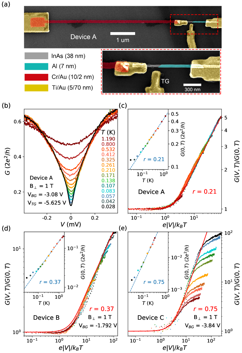
To demonstrate ECB in our device, we first apply an out-of-plane magnetic field () of 1 T (perpendicular to the Al film) to suppress its superconductivity. The device is then equivalent to a normal tunnel junction connected to a dissipative lead. Fig. 1b shows the significant suppression of at low bias and temperature , consistent with the hallmark of ECB (‘dissipative tunneling’). In Fig. 1c, we re-scale all the curves in Fig. 1b (the negative bias branch) using dimensionless units, where they all collapse onto a single universal curve (the red line in Fig. 1c) with minor deviations. The red line is obtained by performing numerical derivative of the expression for the dissipative tunneling of a single tunnel barrier [13]: where is the Boltzmann constant and the Gamma function. is the dissipation strength extracted from the power-law exponent, , of the -dependence for the zero-bias (Fig. 1c inset). For 100 mK, deviates from the power-law (blue line), suggesting a gradual saturation of the electron : fridge of 30 mK roughly corresponds to an electron 50 mK. We used the electron , estimated based on this ‘power-law’ thermometer [42], for the re-scaled x-axis in Fig. 1c for curves of 100 mK.
The dissipation strength, , translates to an effective dissipation resistance k, roughly consistent with our independent estimation of the dissipative resistor 5.46 k. We have also checked similar power-law behaviors in Device B and C, designed with larger dissipative resistors as shown in Fig. 1d and Fig. 1e. The extracted exponent (0.75) for Device B (C) corresponds to an effective dissipation resistance of 9.55 (19.36) k, also roughly consistent with our independent estimation of 7.5 (27.28) k. The deviations might be due to inaccurate estimations of the dissipative resistor (see Sfig. 1) or contributions from other dissipation sources. When the dissipative resistor’s is comparable to the resistance of the InAs-Al tunneling junction (), the effective dissipative resistance should be replaced by [43], also causing sizable deviations. Power-law fits at the other gate voltages (see Sfig. 2) show fluctuations possibly due to reasons mentioned above. In Fig. 1e, we note that at larger bias deviates from the universal red line. This deviation, also expected for Device AB if the bias was large enough, is because that the power-law is only applicable within a finite energy bandwidth [7]. This cut-off energy/frequency is set by where is the junction capacitance which further determines the charging energy of the junction.
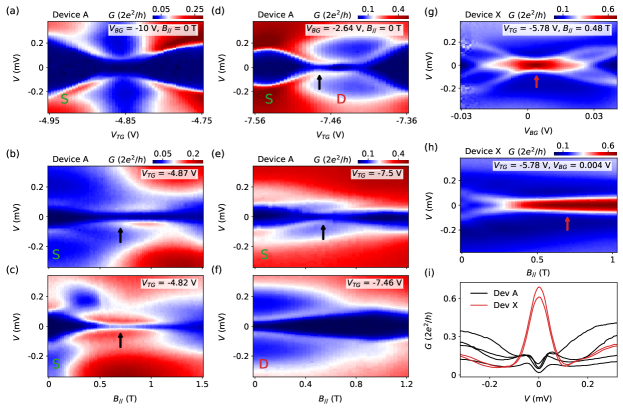
We now set back to zero and study the superconducting behavior in a dissipative environment. In the literature of ‘Majorana nanowires’, the term ‘dissipation’ usually refers to disorder at the InAs-Al interface which causes soft induced superconducting gaps [44, 45]. To avoid confusion, in this paper we refer ‘dissipation’ only to effects caused by the dissipative resistor. In fact for our InAs-Al nanowires (without dissipation), we have shown the atomically abrupt InAs-Al interface [46], hard induced gaps and large ZBPs [26]. Now with the dissipative resistor (Device A), the gap, co-exists with Coulomb blockade, still remains hard (see Sfig. 3). But the coherence peaks are smeared, possibly due to non-equilibrium dissipation. Nevertheless, we can still resolve clean Andreev bound states (ABS) as shown in Fig. 2.
Fig. 2a shows the gate dependence of an ABS in Device A. The two sub-gap levels do not cross, suggesting a singlet ground state [29]. As a result, a magnetic field (, aligned with the nanowire) Zeeman splits the two sub-gap peaks and drives the inner peaks towards zero as shown in Fig. 2bc (the splitting and the outer peaks are sometimes barely visible). In regular devices without a dissipative lead, further increasing can lead to level crossing and ZBP formation as shown in Fig. 2h for Device X. This ZBP due to ABS level crossing is a ubiquitous observation and well established phenomenon [29, 46]. Now back to our Device A with dissipation, Fig. 2bc show that the ‘expected’ ZBPs at the expected crossing points (arrows) are suppressed to split-peaks (see Sfig. 4 ‘waterfall’ plots of line-cuts). This suppression of ZBPs in devices with a strongly dissipative lead is the main observation of the paper. We attribute this observation to the interaction effect (ECB) caused by the dissipative environment. ECB suppresses in a non-uniform way: the suppression is stronger for lower and energy (bias). Therefore, the zero-bias at base is suppressed the most, while the high-bias is less affected, making the expected ZBP to split-peaks [16].
Fig. 2d shows another ABS case where the ground state can be continuously gate tuned from singlet (S) to doublet (D), see labeling. At the singlet-doublet switching point (black arrow), the sub-gap states are expected to cross and form a ZBP in regular devices without dissipation. Here with dissipation, the ‘expected’ ZBP is again suppressed. Fig. 2ef show the -dependence of the ABS. For the singlet case (Fig. 2e), the two peaks merge towards zero at the field (black arrow) where the ‘expected’ ZBP is suppressed. In Fig. 2f, the two peaks move away from zero energy when increasing , consistent with the doublet behavior [29]. For additional - and gate-scans of the singlet and doublet ABSs in Fig. 2a-f, see Sfig. 5 and Sfig. 6.
For comparison, we show a ZBP data set in control Device X (without the dissipative resistor) in Fig. 2gh. We have also applied a perpendicular of 1 T for Device X to suppress its superconductivity and test/confirm no-power law suppression as Fig. 1 (see Sfig. 7). The ZBP, formed from level merging, shows some robustness (non-split) in gate (Fig. 2g) and (Fig. 2h) scans. The ZBP is not quantized, ruling out the topological origin, see Sfig. 8 additional scans. In Fig. 2i we show line-cuts to contrast the suppressed ZBPs from Device A (black curves) and ZBPs from Device X (red curves).
We now study the -dependence of the ABS with dissipation. Fig. 3a shows the ABS from Fig. 2d with T, measured at base . The measurement was then repeated at different s (see Sfig. 9). Fig. 3b shows a near-zero energy ABS line-cut from Fig. 3a for different s (only four curves are plotted for clarity). The solid lines are theory simulations using the formula , where is the Fermi distribution function. For convenience, note the unit conversion between and for and . We assume the mK curve as to calculate for different s which should be valid for much larger than 20 mK. The simulation, only taking thermal averaging effect into account, shows significant deviations from data, suggesting that thermal averaging alone can not explain the -dependence of this near zero-energy ABS. The measured larger than the thermal simulation suggests the lifting of ECB suppression at higher s.
We further plot the zero-bias of this line-cut for all s in Fig. 3c (black dots), and find a power-law behavior with an exponent of , close to assuming = 0.21. At other gate voltages where the ABS has finite energies, we also find similar power-law-like behavior within an intermediate -range (from 60 mK to 300 mK), see the brown and orange dots as two examples with exponents of and . Fig. 3a (lower panel) shows the exponent at different gate voltages (in the left- and right-most regions without data, we can not find a reasonable power-law-like fit). For -dependence of the singlet ABS (Fig. 2a-c) and more power-law-like fittings, see Sfig. 9.
In a recent theory work [47], we have studied dissipative tunneling of ABS mediated by Andreev reflection and showed that the power-law exponent can be or , corresponding to coherent or incoherent Andreev reflection processes. Other intermediate exponent values between , and (corresponding to normal tunneling due to e.g. soft gap or gap-closing) could also be achieved depending on the mixture between different processes. Whether our observation here corresponds to the theory situations discussed above remains as an open question and requires further systematic study. For example, we note the -range of the power-law in Fig. 3c for is not large (only half a decade), therefore hard to be used as an exclusive tool for theory understanding. For mK, the data deviation is possibly due to the saturation of electron . For 300 mK, the deviation is probably due to the softening of the superconducting gap where incoherence Andreev reflection or normal tunneling due to quasi-particle poisoning starts to contribute. Nevertheless, optimizations are needed for better power-laws to fully understand ‘dissipative Andreev tunneling’.
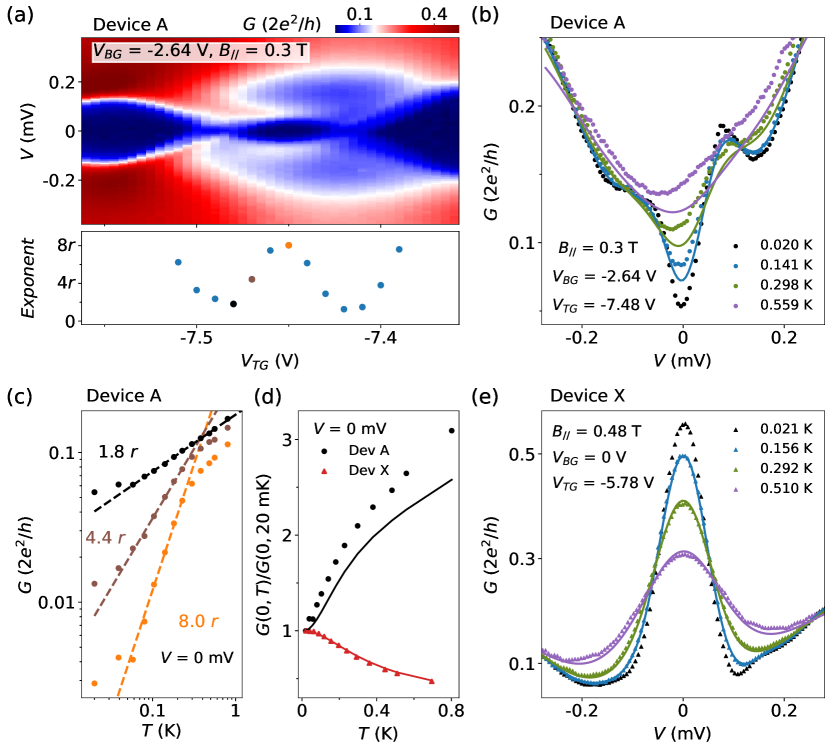
In Fig. 3d we re-plot the black dots from Fig. 3c and show the significant deviation from the thermal averaging simulation (black line). This deviation is also observable in Fig. 3b. By contrast, in our control Device X (without dissipation), the -dependence of ZBP shows reasonable agreement with the simulation (without any fitting parameter) for both zero bias (Fig. 3d red) and finite bias (Fig. 3e), suggesting that thermal averaging is indeed the dominating effect in the -dependence of zero-energy ABS in Device X. This sharp contrast between Fig. 3b and Fig. 3e confirms the Fermi liquid -dependence for Device X (without dissipation) and suggests the non-Fermi liquid -dependence in Device A (with dissipation). We note the softening of the superconducting gap at higher , not taken into account in the simulation, could also cause small deviations between data and simulation in Device X especially for non-zero energy ABS (see SFig. 8). Therefore, we restrict our thermal averaging simulation to only zero or near-zero energy ABS.
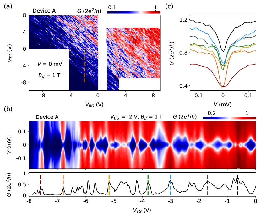
In Fig. 2 we have presented two examples of ABS to show that the expected ZBPs can be suppressed due to dissipation. In fact, similar behavior is observed in most of the parameter ranges explored in Device A. Fig. 4a shows the zero-bias of Device A over a large gate voltage range at a parallel field of 1 T where ZBPs are likely to occur [26]. The dense diagonal lines suggest formation of unintentional quantum dots and possibly ABSs. However, further bias scan (Fig. 4b) over a typical line-cut in Fig. 4a resolves no ZBP at all (see Fig. 4c line-cuts). We have also checked other regions of the parameter space in Device A, and did not find any clear ZBPs (see Sfig. 10). This absence of ZBP in almost all the explored parameter regions is dramatically different from our previous experience where without dissipation, ZBPs can be easily and routinely found [46, 26]. Very rarely, very faint and small ZBP-like feature can be barely visible, see Sfig. 10 the only case we found in Device A. For Device B and C, we also did not find any ZBP (see Sfig. 3). We note this observation is not inconsistent with our expectation based on previous experience in regular devices where 1) non-quantized ZBPs are ubiquitous and can be easily found in every device [48], therefore suppressed by dissipation; 2) large ZBPs near the quantized value (resolving plateau-like feature) are rare and not in every device [25, 26].
The dissipation resistance or strength is a crucial parameter. If is too strong (larger than 1/2), theory [16] predicts that all ZBPs (including the ones due to Majoranas) will be suppressed. If is less than 1/2, Majorana or quasi-Majorana ZBPs could survive while trivial ZBPs will be suppressed (the latter is demonstrated in this paper). But this does not mean that can be arbitrarily small. For example, if is approaching zero, corresponding to the case without dissipation (Device X), apparently trivial ZBPs will revive. This weak or intermediate dissipative regime will be explored in a future separate work. We identify the -value of 0.21 or larger in this paper as the strong dissipation regime based on the observation that most of ABS ZBPs can be suppressed.
To summarize, we have implemented a strongly dissipative lead in our InAs-Al hybrid nanowire devices. The dissipative environment, confirmed by the observation of environmental Coulomb blockade, power-laws and non-Fermi liquid temperature dependence, can significantly suppress the Andreev bound state zero bias peaks, which ubiquitously exist in hybrid nanowires and disturb Majorana detections, see also [47] our recent related theory work. Our device set-up could serve as a possible filter to narrow down the ZBP phase diagram in future Majorana searches [16, 49, 50, 51].
Acknowledgment We thank Gleb Finkelstein, Harold Baranger and Chung-Ting Ke for valuable discussions. Raw data and processing codes within this paper are available at https://doi.org/10.5281/zenodo.5630076. This work is supported by Tsinghua University Initiative Scientific Research Program, National Natural Science Foundation of China (Grant Nos. 11974198, 92065106 61974138), Beijing Natural Science Foundation (Grant No. 1192017). D. P. acknowledges the support from Youth Innovation Promotion Association, Chinese Academy of Sciences (No. 2017156).
References
- Delsing et al. [1989] P. Delsing, K. K. Likharev, L. S. Kuzmin, and T. Claeson, Effect of high-frequency electrodynamic environment on the single-electron tunneling in ultrasmall junctions, Phys. Rev. Lett. 63, 1180 (1989).
- Devoret et al. [1990] M. H. Devoret, D. Esteve, H. Grabert, G.-L. Ingold, H. Pothier, and C. Urbina, Effect of the electromagnetic environment on the coulomb blockade in ultrasmall tunnel junctions, Phys. Rev. Lett. 64, 1824 (1990).
- Cleland et al. [1990] A. N. Cleland, J. M. Schmidt, and J. Clarke, Charge fluctuations in small-capacitance junctions, Phys. Rev. Lett. 64, 1565 (1990).
- Ingold and Nazarov [1992] G. L. Ingold and Y. V. Nazarov, Single Charge Tunnelling: Coulomb Blockade Phenomena in Nanostructures (Springer, 1992) (eds Grabert, H. and Devoret, M. H.) 21-107.
- Flensberg et al. [1992] K. Flensberg, S. M. Girvin, M. Jonson, D. R. Penn, and M. D. Stiles, Quantum mechanics of the electromagnetic environment in the single-junction coulomb blockade, Physica Scripta T42, 189 (1992).
- Joyez et al. [1998] P. Joyez, D. Esteve, and M. H. Devoret, How is the coulomb blockade suppressed in high-conductance tunnel junctions?, Phys. Rev. Lett. 80, 1956 (1998).
- Zheng et al. [1998] W. Zheng, J. Friedman, D. Averin, S. Han, and J. Lukens, Observation of strong coulomb blockade in resistively isolated tunnel junctions, Solid State Communications 108, 839 (1998).
- Chang [2003] A. M. Chang, Chiral luttinger liquids at the fractional quantum hall edge, Rev. Mod. Phys. 75, 1449 (2003).
- Safi and Saleur [2004] I. Safi and H. Saleur, One-channel conductor in an ohmic environment: Mapping to a tomonaga-luttinger liquid and full counting statistics, Phys. Rev. Lett. 93, 126602 (2004).
- Jezouin et al. [2013] S. Jezouin, M. Albert, F. Parmentier, A. Anthore, U. Gennser, A. Cavanna, I. Safi, and F. Pierre, Tomonaga–luttinger physics in electronic quantum circuits, Nature Communications 4, 1 (2013).
- Anthore et al. [2018] A. Anthore, Z. Iftikhar, E. Boulat, F. D. Parmentier, A. Cavanna, A. Ouerghi, U. Gennser, and F. Pierre, Circuit quantum simulation of a tomonaga-luttinger liquid with an impurity, Phys. Rev. X 8, 031075 (2018).
- Bomze et al. [2009] Y. Bomze, H. Mebrahtu, I. Borzenets, A. Makarovski, and G. Finkelstein, Resonant tunneling in a dissipative environment, Physical Review B 79, 241402 (2009).
- Mebrahtu et al. [2012] H. T. Mebrahtu, I. V. Borzenets, D. E. Liu, H. Zheng, Y. V. Bomze, A. I. Smirnov, H. U. Baranger, and G. Finkelstein, Quantum phase transition in a resonant level coupled to interacting leads, Nature 488, 61 (2012).
- Mebrahtu et al. [2013] H. Mebrahtu, I. Borzenets, H. Zheng, Y. V. Bomze, A. Smirnov, S. Florens, H. Baranger, and G. Finkelstein, Observation of majorana quantum critical behaviour in a resonant level coupled to a dissipative environment, Nature Physics 9, 732 (2013).
- Liu et al. [2014] D. E. Liu, H. Zheng, G. Finkelstein, and H. U. Baranger, Tunable quantum phase transitions in a resonant level coupled to two dissipative baths, Physical Review B 89, 085116 (2014).
- Liu [2013] D. E. Liu, Proposed method for tunneling spectroscopy with ohmic dissipation using resistive electrodes: a possible majorana filter, Physical Review Letters 111, 207003 (2013).
- Lutchyn et al. [2010] R. M. Lutchyn, J. D. Sau, and S. Das Sarma, Majorana fermions and a topological phase transition in semiconductor-superconductor heterostructures, Phys. Rev. Lett. 105, 077001 (2010).
- Oreg et al. [2010] Y. Oreg, G. Refael, and F. von Oppen, Helical liquids and majorana bound states in quantum wires, Phys. Rev. Lett. 105, 177002 (2010).
- Lutchyn et al. [2018] R. M. Lutchyn, E. P. Bakkers, L. P. Kouwenhoven, P. Krogstrup, C. M. Marcus, and Y. Oreg, Majorana zero modes in superconductor–semiconductor heterostructures, Nature Reviews Materials 3, 52 (2018).
- Prada et al. [2020] E. Prada, P. San-Jose, M. W. de Moor, A. Geresdi, E. J. Lee, J. Klinovaja, D. Loss, J. Nygård, R. Aguado, and L. P. Kouwenhoven, From andreev to majorana bound states in hybrid superconductor–semiconductor nanowires, Nature Reviews Physics 2, 575 (2020).
- Mourik et al. [2012] V. Mourik, K. Zuo, S. M. Frolov, S. Plissard, E. P. Bakkers, and L. P. Kouwenhoven, Signatures of majorana fermions in hybrid superconductor-semiconductor nanowire devices, Science 336, 1003 (2012).
- Deng et al. [2016] M. Deng, S. Vaitiekėnas, E. B. Hansen, J. Danon, M. Leijnse, K. Flensberg, J. Nygård, P. Krogstrup, and C. M. Marcus, Majorana bound state in a coupled quantum-dot hybrid-nanowire system, Science 354, 1557 (2016).
- Gül et al. [2018] Ö. Gül, H. Zhang, J. D. Bommer, M. W. de Moor, D. Car, S. R. Plissard, E. P. Bakkers, A. Geresdi, K. Watanabe, T. Taniguchi, et al., Ballistic majorana nanowire devices, Nature Nanotechnology 13, 192 (2018).
- Nichele et al. [2017] F. Nichele, A. C. Drachmann, A. M. Whiticar, E. C. O’Farrell, H. J. Suominen, A. Fornieri, T. Wang, G. C. Gardner, C. Thomas, A. T. Hatke, et al., Scaling of majorana zero-bias conductance peaks, Physical Review Letters 119, 136803 (2017).
- Zhang et al. [2021] H. Zhang, M. W. de Moor, J. D. Bommer, D. Xu, G. Wang, N. van Loo, C.-X. Liu, S. Gazibegovic, J. A. Logan, D. Car, R. L. M. Op het Veld, P. J. van Veldhoven, S. Koellinga, M. A. Verheijen, M. Pendharkar, D. J. Pennachio, B. Shojaei, J. S. Lee, C. J. Palmstrøm, E. P. Bakkers, S. Das Sarma, and L. P. Kouwenhoven, Large zero-bias peaks in insb-al hybrid semiconductor-superconductor nanowire devices, arXiv: 2101.11456 (2021).
- Song et al. [2021] H. Song, Z. Zhang, D. Pan, D. Liu, Z. Wang, Z. Cao, L. Liu, L. Wen, D. Liao, R. Zhuo, D. E. Liu, R. Shang, J. Zhao, and H. Zhang, Large zero bias peaks and dips in a four-terminal thin inas-al nanowire device, arXiv: 2107.08282 (2021).
- Sengupta et al. [2001] K. Sengupta, I. Žutić, H.-J. Kwon, V. M. Yakovenko, and S. D. Sarma, Midgap edge states and pairing symmetry of quasi-one-dimensional organic superconductors, Physical Review B 63, 144531 (2001).
- Law et al. [2009] K. T. Law, P. A. Lee, and T. K. Ng, Majorana fermion induced resonant andreev reflection, Physical Review Letters 103, 237001 (2009).
- Lee et al. [2014] E. J. Lee, X. Jiang, M. Houzet, R. Aguado, C. M. Lieber, and S. De Franceschi, Spin-resolved andreev levels and parity crossings in hybrid superconductor–semiconductor nanostructures, Nature Nanotechnology 9, 79 (2014).
- Prada et al. [2012] E. Prada, P. San-Jose, and R. Aguado, Transport spectroscopy of n s nanowire junctions with majorana fermions, Physical Review B 86, 180503 (2012).
- Kells et al. [2012] G. Kells, D. Meidan, and P. Brouwer, Near-zero-energy end states in topologically trivial spin-orbit coupled superconducting nanowires with a smooth confinement, Physical Review B 86, 100503 (2012).
- Liu et al. [2017a] C.-X. Liu, J. D. Sau, T. D. Stanescu, and S. D. Sarma, Andreev bound states versus majorana bound states in quantum dot-nanowire-superconductor hybrid structures: Trivial versus topological zero-bias conductance peaks, Physical Review B 96, 075161 (2017a).
- Cao et al. [2019] Z. Cao, H. Zhang, H.-F. Lü, W.-X. He, H.-Z. Lu, and X. C. Xie, Decays of majorana or andreev oscillations induced by steplike spin-orbit coupling, Phys. Rev. Lett. 122, 147701 (2019).
- Liu et al. [2012] J. Liu, A. C. Potter, K. T. Law, and P. A. Lee, Zero-bias peaks in the tunneling conductance of spin-orbit-coupled superconducting wires with and without majorana end-states, Phys. Rev. Lett. 109, 267002 (2012).
- Liu et al. [2018] D. E. Liu, E. Rossi, and R. M. Lutchyn, Impurity-induced states in superconducting heterostructures, Phys. Rev. B 97, 161408 (2018).
- Pan and Das Sarma [2020] H. Pan and S. Das Sarma, Physical mechanisms for zero-bias conductance peaks in majorana nanowires, Phys. Rev. Research 2, 013377 (2020).
- Pan et al. [2021] H. Pan, C.-X. Liu, M. Wimmer, and S. Das Sarma, Quantized and unquantized zero-bias tunneling conductance peaks in majorana nanowires: Conductance below and above , Phys. Rev. B 103, 214502 (2021).
- Ahn et al. [2021] S. Ahn, H. Pan, B. Woods, T. Stanescu, and S. Das Sarma, Estimating disorder and its adverse effects in semiconductor majorana nanowires, arXiv:2109.00007 (2021).
- Vuik et al. [2019] A. Vuik, B. Nijholt, A. Akhmerov, and M. Wimmer, Reproducing topological properties with quasi-majorana states, SciPost Physics 7, 061 (2019).
- Moore et al. [2018] C. Moore, C. Zeng, T. D. Stanescu, and S. Tewari, Quantized zero-bias conductance plateau in semiconductor-superconductor heterostructures without topological majorana zero modes, Physical Review B 98, 155314 (2018).
- Das Sarma and Pan [2021] S. Das Sarma and H. Pan, Disorder-induced zero-bias peaks in majorana nanowires, Phys. Rev. B 103, 195158 (2021).
- Mebrahtu [2012] H. T. Mebrahtu, Electron transport through carbon nanotube quantum dots in a dissipative environment, Ph.D. thesis, Duke University (2012).
- Flensberg and Jonson [1991] K. Flensberg and M. Jonson, Quantum fluctuations and charging effects in small tunnel junctions, Phys. Rev. B 43, 7586 (1991).
- Takei et al. [2013] S. Takei, B. M. Fregoso, H.-Y. Hui, A. M. Lobos, and S. D. Sarma, Soft superconducting gap in semiconductor majorana nanowires, Physical Review Letters 110, 186803 (2013).
- Liu et al. [2017b] C.-X. Liu, J. D. Sau, and S. Das Sarma, Role of dissipation in realistic majorana nanowires, Phys. Rev. B 95, 054502 (2017b).
- Pan et al. [2020] D. Pan, H. Song, S. Zhang, L. Liu, L. Wen, D. Liao, R. Zhuo, Z. Wang, Z. Zhang, S. Yang, J. Ying, W. Miao, R. Shang, H. Zhang, and J. Zhao, In situ epitaxy of pure phase ultra-thin inas-al nanowires for quantum devices, arXiv: 2011.13620 (2020).
- Liu et al. [2021] D. Liu, G. Zhang, Z. Cao, H. Zhang, and D. E. Liu, Universal conductance scaling of andreev reflections using a dissipative probe, arXiv: 2110.10039 (2021).
- de Moor et al. [2018] M. W. de Moor, J. D. Bommer, D. Xu, G. W. Winkler, A. E. Antipov, A. Bargerbos, G. Wang, N. Van Loo, R. L. O. het Veld, S. Gazibegovic, et al., Electric field tunable superconductor-semiconductor coupling in majorana nanowires, New Journal of Physics 20, 103049 (2018).
- Liu et al. [2020] D. Liu, Z. Cao, H. Zhang, and D. E. Liu, Revealing the nonlocal coherent nature of majorana devices from dissipative teleportation, Physical Review B 101, 081406 (2020).
- Zhang and Spånslätt [2020] G. Zhang and C. Spånslätt, Distinguishing between topological and quasi majorana zero modes with a dissipative resonant level, Physical Review B 102, 045111 (2020).
- Zhang et al. [2019] H. Zhang, D. E. Liu, M. Wimmer, and L. P. Kouwenhoven, Next steps of quantum transport in majorana nanowire devices, Nature Communications 10, 1 (2019).