Superconducting diode effect and interference patterns in Kagome CsV3Sb5
Abstract
The interplay among frustrated lattice geometry, nontrivial band topology and correlation yields rich quantum states of matter in Kagome systems 1; 2. A series of recent members in this family, V3Sb5 (= K, Rb, Cs), exhibit a cascade of symmetry-breaking transitions 3, involving the 3Q chiral charge ordering 4; 5; 6; 7; 8, electronic nematicity 9; 10, roton pair-density-wave 11 and superconductivity 12. The nature of the superconducting order is yet to be resolved. Here, we report an indication of chiral superconducting domains with boundary supercurrents in intrinsic CsV3Sb5 flakes. Magnetic field-free superconducting diode effect is observed with polarity modulated by thermal histories, suggesting dynamical superconducting order domains in a spontaneous time-reversal symmetry breaking background. Strikingly, the critical current exhibits the double-slit superconducting interference patterns when subjected to an external magnetic field. Characteristics of the patterns are modulated by thermal cycling. These phenomena are proposed as a consequence of periodically modulated supercurrents flowing along certain domain boundaries constrained by fluxoid quantization. Our results imply a chiral superconducting order, opening a potential for exploring exotic physics, e.g. Majorana zero modes, in this intriguing topological Kagome system.
Chiral superconductors (SC), characterized by complex order parameters, break time-reversal symmetry (TRS) spontaneously. Certain types of chiral SCs are topologically non-trivial whose gap functions exhibit phase winding over the Fermi surface. They allow for exploring chiral edge states and Majorana zero modes, showing a promise for fault-tolerant topological quantum computation 13. A well-known example exhibiting chiral pairing symmetry is the superfluid 3He-A phase 14. In electronic materials, evidence of TRS breaking has been reported 15; 16; 17; 18, including Sr2RuO4 15, UPt3 16 and UTe2 17. Nevertheless, an unequivocal demonstration of chiral edge supercurrent () at SC domain boundaries is still a pending target.
V3Sb5 (=K, Rb, Cs) exhibit a rich phase diagram featured by the intricate interplay among multiple intertwined orders 4; 5; 6; 7; 8; 9; 10; 19; 11. This hints the possibility of unconventional SC 20; 7; 11, yet the pairing symmetry remains unclear 21; 22; 23; 24; 25; 26; 27. Accumulated evidence 23; 24; 25; 26; 27, including nuclear quadrupole resonance 23, tunnel diode oscillator 24, electron irradiation 25 and angle-resolved photoemission spectroscopy 26, surprisingly indicates the presence of nodeless, spin-singlet, and nearly isotropic SC gaps. From a theoretical perspective, a chiral SC state with a fully gapped composite gap function has been proposed in literature 28; 29; 30. Relevant clues to this are elusive 6; 31; 22; 26, derived exclusively from muon spin spectroscopy (SR) that detects signals of broken TRS. Phase-sensitive probes are crucial but still lacking. Here, we present signatures of chiral SC domains in CsV3Sb5 via phase-sensitive measurements.
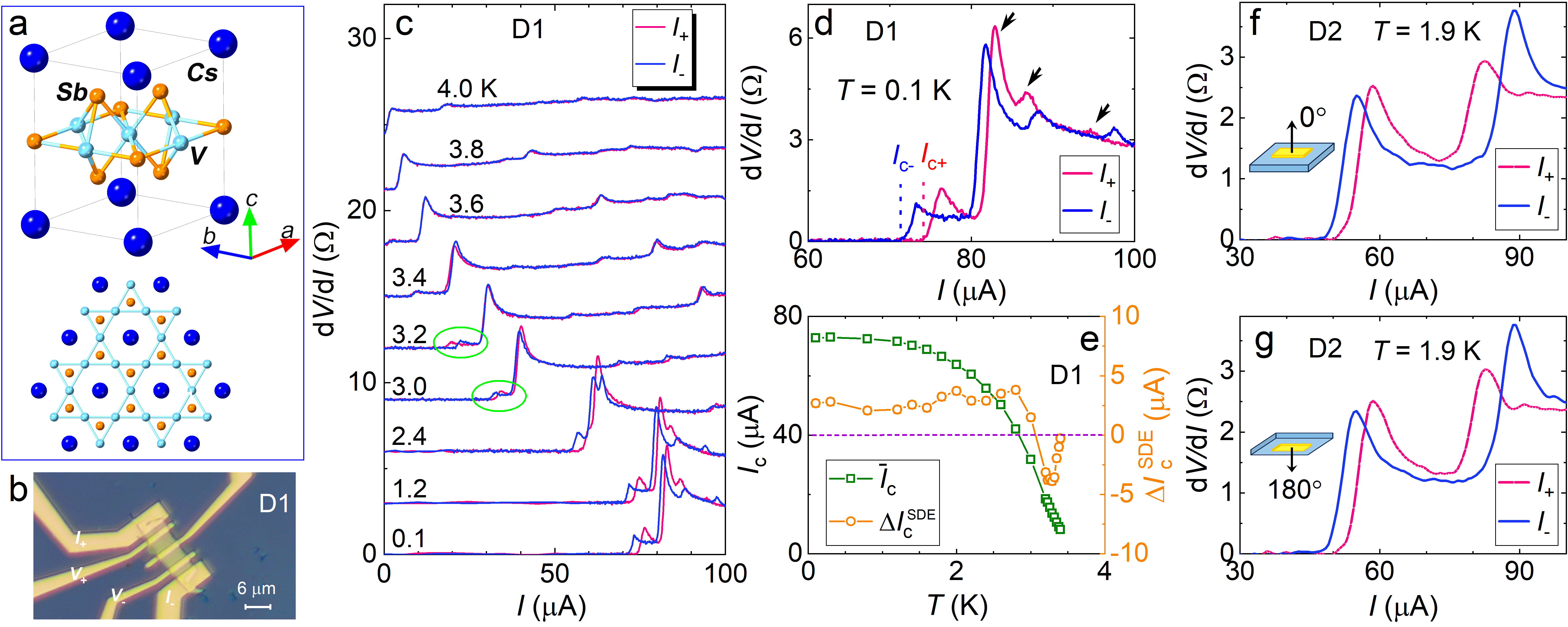
CsV3Sb5 hosts a hexagonal structure, composed of alternating stacks of V3Sb5 slabs and Cs layers, among which vanadium ions form the Kagome net, seen in Fig. 1a. For the measurements, three devices (D1-D3) were fabricated by mechanically exfoliating nanoflakes from high-quality single crystals. The basic transport properties are presented in Extended Data Fig. 1.
Zero-field superconducting diode effect
The chiral SC was inspected by observing the SC diode effect (SDE), which depicts an asymmetry of the critical current () with respect to the direction of current flow in the absence of TRS and inversion symmetry (IRS) 32; 33. TRS and IRS are disrupted either internally or externally. In the case of internal TRS breaking, magnetic field ()-free SDEs 34; 35; 36 are realized, in turn reflecting the nature of pairing symmetry 33. To examine intrinsic properties, non-SC contacts were made by gold deposition, seen in Fig. 1b. The cryostat was warmed up to room temperature () to fully release residual flux trapped in the SC magnet prior to experiments. In Supplementary Note 1, additional procedures were implemented to further eliminate any remaining field.
In Fig. 1c, the differential resistance (d/d) for D1 was measured by sweeping the d.c. current () at zero and various . evolves with the reduction of along with a noticeable inequivalence between the positive () and negative () bias regimes. A magnified curve at K is specified in Fig. 1d, in which along the positive direction is larger than along the negative one (A), indicating non-reciprocity. Additionally, several non-reciprocal transition features (marked by arrows) are observed above . Its relation to SC domain structures will be explained later. Fig. 1e displays the average and versus . As declines, shows a peculiar sign switching slightly below the SC transition temperature ( K), as indicated by circles in Fig. 1c, and eventually its polarity becomes stable. This polarity variation is weird, distinct from what was reported 33; 35. In Extended Data Fig. 2, the SDE polarity could be reversed after thermal cycling from slightly above , which also shows the magnitude alteration of and . Relevant data, including half-wave rectification, are shown in Extended Data Fig. 3, 4. It is noteworthy that the SDE signals remained unchanged even when the setup was reversed in Fig. 1f and g, underscoring the prominent role played by the spontaneous TRS-breaking, instead of from the environment. See more discussion in Supplementary Note 1.
The presence of thermal switching and polarity variation in zero-field SDEs hints the existence of dynamic orders in an internal TRS-breaking background. A plausible candidate is chiral SC domains, which will be further elucidated below. This finding is hardly explained by the chiral charge order inherited from the normal state (see discussion in Methods).
Superconducting interference patterns
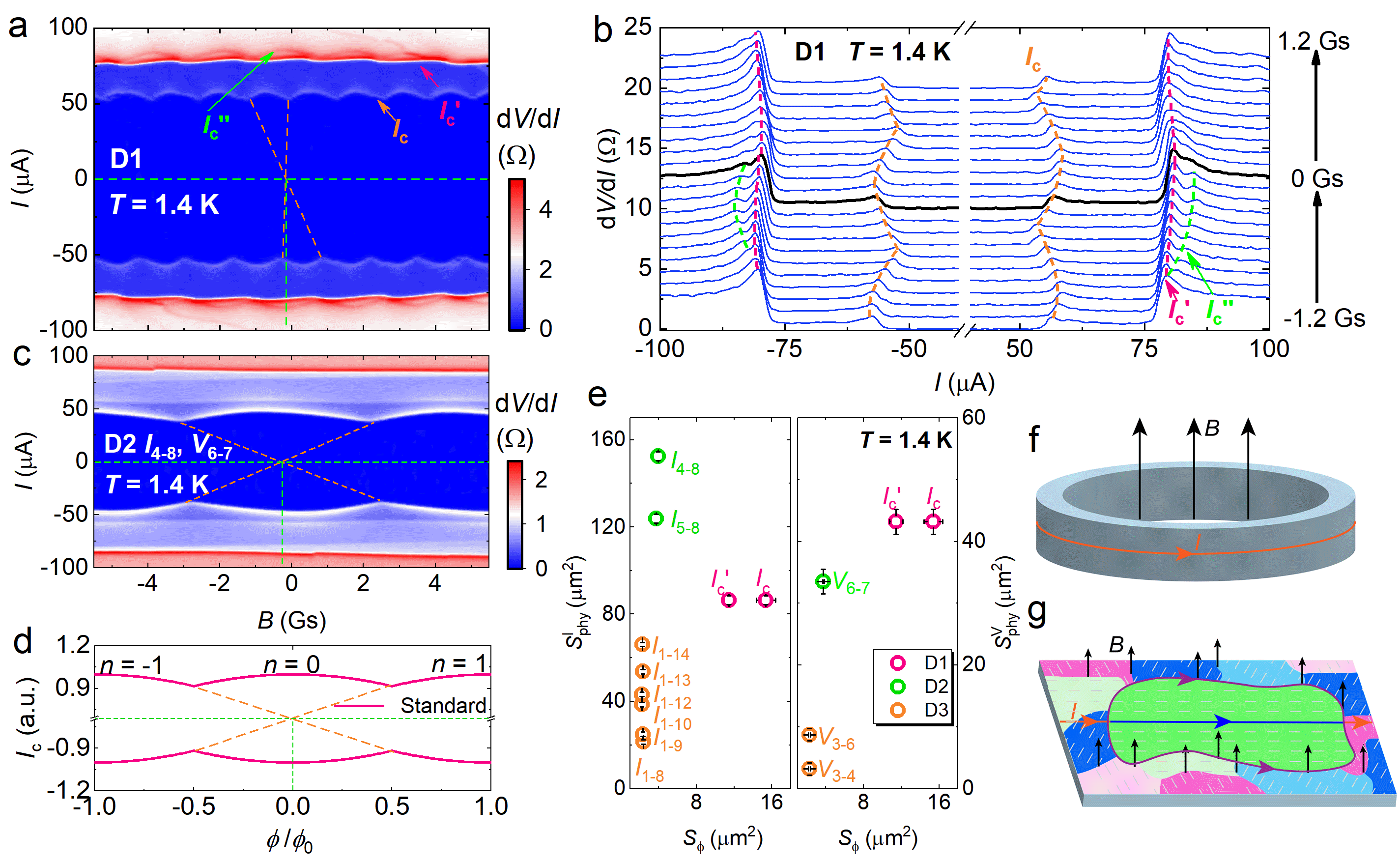
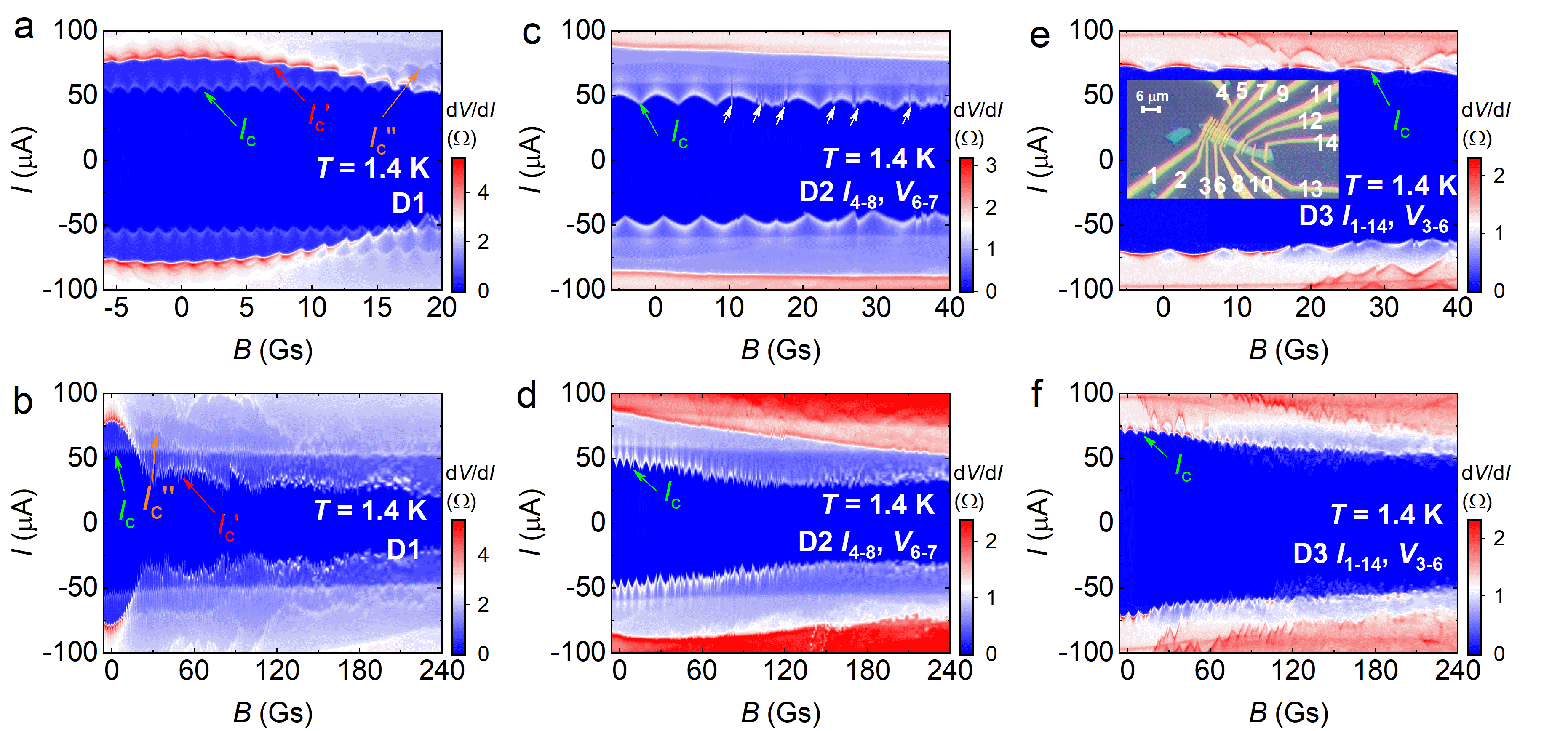
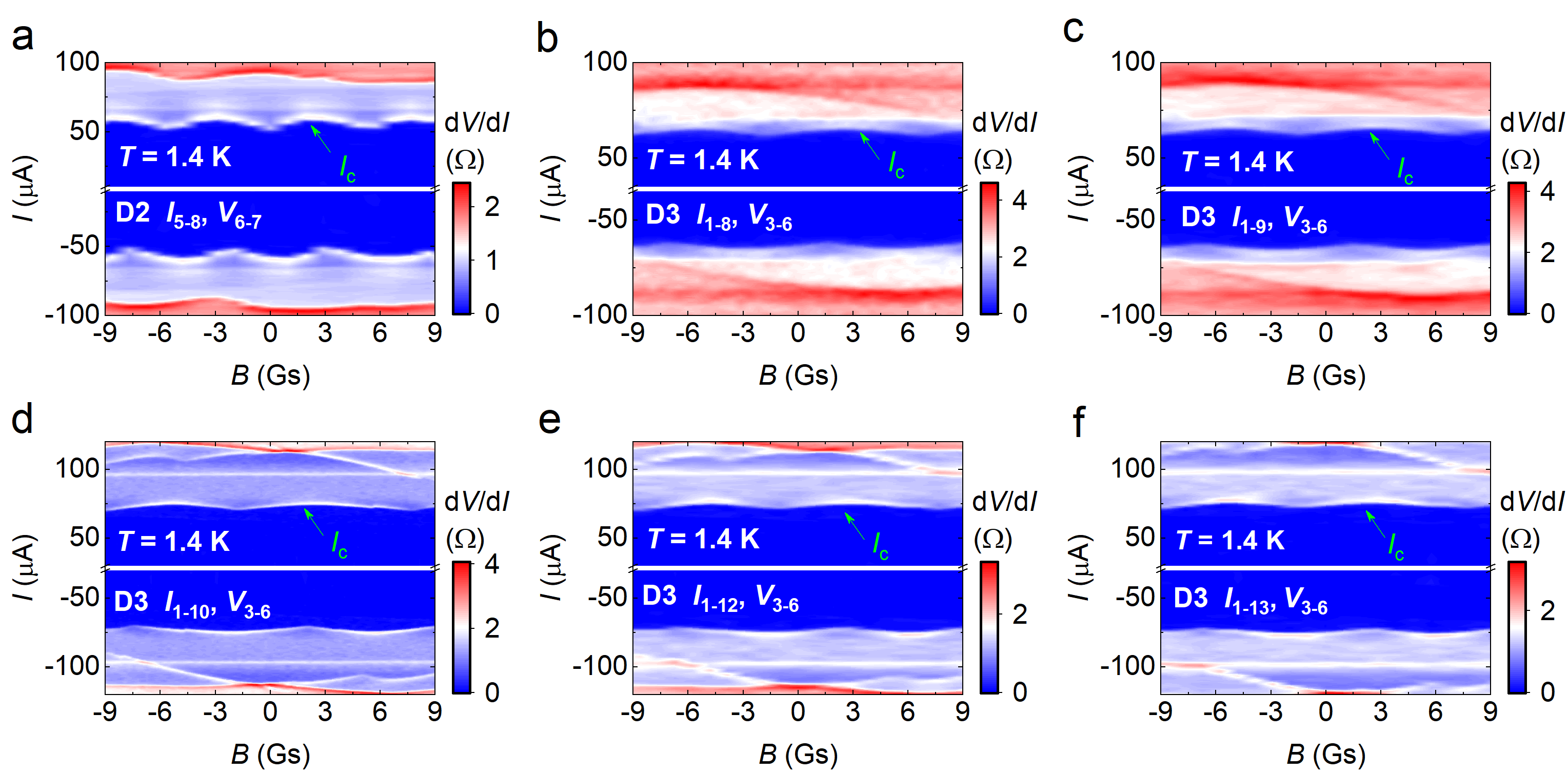
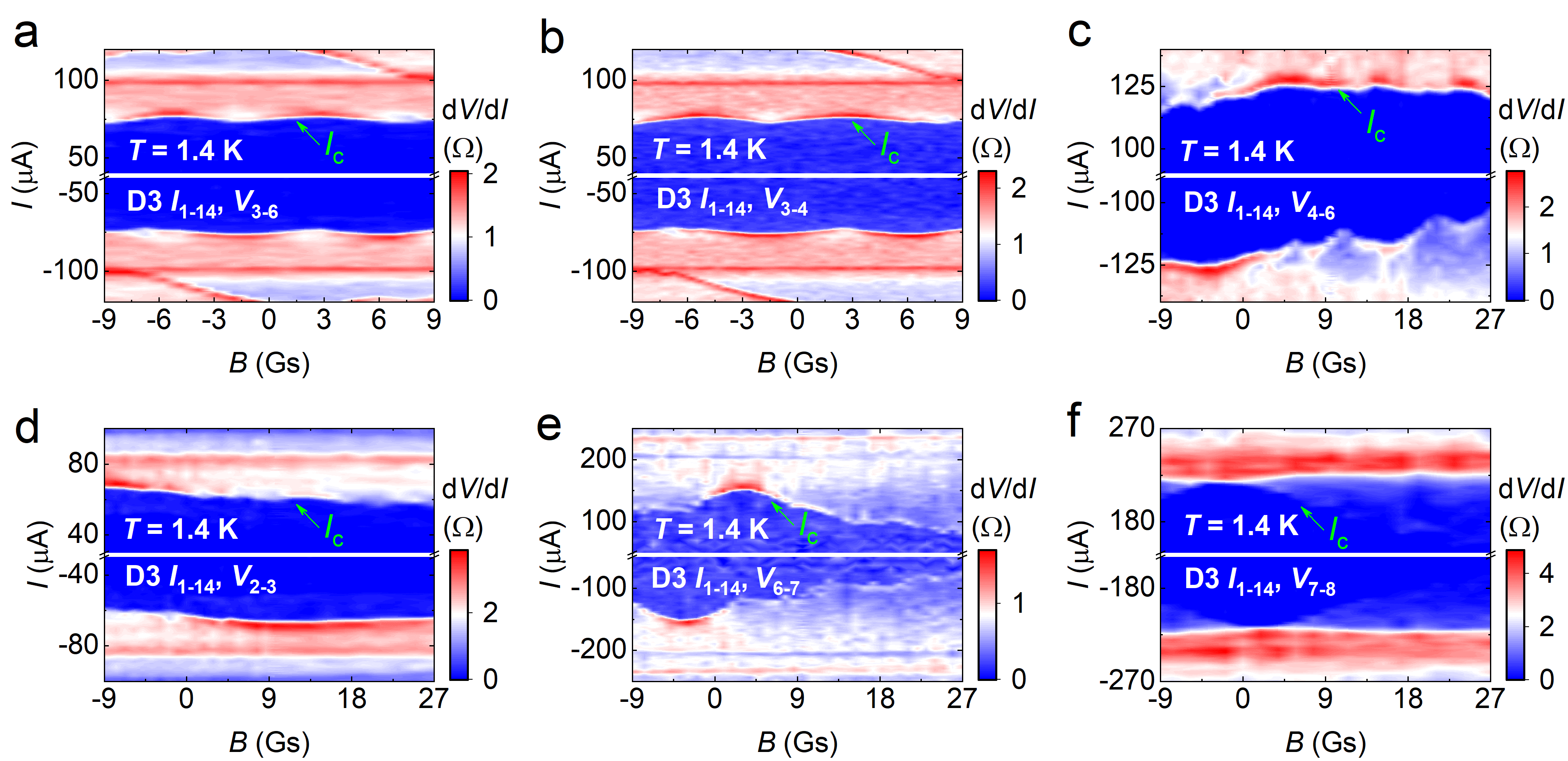
In Fig. 2a, b, we measured at selective values of for D1 and plotted its color map in the - plane. Intriguingly, three sets of periodic oscillation profiles (, and ) are resolved in Fig. 2a, traced by three transition peaks marked by dashed curves in Fig. 2b. Similar patterns with distinct periodicity for D2 are presented in Fig. 2c. More data are in Extended Data Fig. 5-7.
Such double-slit patterns vividly imitate the SC interference patterns (SIPs), which would be obtained from a Little-Parks (LP) device as depicted in Fig. 2d. In such a device, the magnetic flux threading in hollow regions modulates the loop supercurrent, as sketched in Fig. 2f 37. The fluxoid quantization within an enclosed area leads to the superfluid velocity , where is the Ginzburg-Landau (GL) effective mass; is the loop circumference; is the closest integer to with the flux quantum and the flux enclosed by the loop; is the field threading area. It subsequently leads to a modulation of the SC condensation wavefunction as . Then, the variation of the GL critical current is yielded as (see more discussion in Supplementary Note 2):
| (1) |
where is the GL coherence length and is a constant of order one.
It seems counterintuitive that such phenomena exist in unpatterned SC devices as in our case. A plausible explanation may lie in the existence of edge supercurrent () forming closed loop structures at certain boundaries 38. According to the oscillation period () extracted from Fig. 2a, c and Extended Data Fig. 6, 7, is calculated through and is compared with , the physical area enclosed by the current/voltage electrodes, in Fig. 2e. Note that is detected by varying the current (voltage) terminals, while keeping the voltage (current) terminals unchanged for a single device. is much smaller than and . No scaling relationships are observed among them. This finding suggests that flows along a specific boundary within the sample 38, aligning with the expectation of chiral SC domains.
In a chiral SC, domain structures between opposite chiralities are often established due to spontaneous symmetry breaking 39. For CsV3Sb5, we will argue below that there is a network of domain walls guiding the flow of (see details in Discussion). At the walls, SC order parameters are relatively suppressed compared to the bulk 18. Thus, the magnetic flux passes through the walls and penetrates the domain on the scale of the Pearl length , where is the London length. Given (0 K)m 31, one yields m for D1 with the thickness nm, which is longer than the domain length scale (), indicating the penetration of flux throughout the domain. The edge supercurrent flows along the wall such that the domain enclosed by the supercurrent loop acts like a hollow (weak shielding of ) that serves as a basis for the LP effect, as illustrated in Fig. 2g. In Supplementary Note 3, we discuss that the circulating supercurrent occurring in the bulk does not induce oscillation patterns.
The preceding discussion primarily revolves around domain boundaries, by assuming a priori that the edge and bulk wave functions ( and ) are treated separately. Indeed, the applied current () passes through both the domain bulk () and edge. As approaches to , is self-distributed such that both the boundary and bulk regions tend toward the normal state. We propose that the sharp double-slit SIPs stems from the contribution of , and gives rise to a slow, broad evolution of , as shown in Extended Data Fig. 5b. In the figure, the double-slit SIP is enveloped by a broader Fraunhofer-like pattern, likely induced by a local Josephson junction between neighboring domains, displaying the superposition of domain edge and bulk contributions. See more discussion in the Supplementary Note 4, 5 and Methods.
Note that is not solely determined by the intrinsic critical current, but rather influenced by the connection strength between SC domains. The randomness in domain distribution and the spatial variation in the connection strength lead to the variation of across different voltage terminals in Extended Data Fig. 4 as well as the multiple transition features in Fig. 1d. The dynamics of domains account for the modulation after thermal cycling in Extended Data Fig. 2. In Extended Data Fig. 7, the sharp SIP exists only between terminals , while others show obscure or even indiscernible patterns. This suggests specific domain structure requirements for observing SIPs, which, we consider, requires a SC domain of suitable dimensions (about 10 m2) and regular geometries, preferably hosting a discrete distinct from the surrounding region in series. Discussion about the possibility of other scenarios is presented in Methods.
Broken time-reversal and inversion symmetry
Upon close inspection of SIPs in Fig. 2a, c, we discern a slight shift of the pattern symmetry center, marked by the intersection of dashed lines, compared to the standard model in Fig. 2d. Its deviation from zero field, defined as , signifies a broken TRS 40. In Supplementary Fig. 3, SIPs at and configurations show indiscernible phase differences with the positive flux direction fixed relative to the flipped sample, indicating the predominant role of internal in determining the phase. In Supplementary Fig. 4, sweeping field within a range of Gs does not induce vortex trapping. Therefore, arises from an intrinsic TRS-breaking effect.
The measured ranges from negligibly small to about 0.8 Gs in Supplementary Fig. 3a. The maximum is about threefold the internal magnetic field detected by SR in the charge order phase 6, which is considered as a chiral flux phase composed of clockwise and anti-clockwise flux loops at the lattice sites in CsV3Sb5 41. SR detects local field created by the imbalances of fluxes. The average at the micron scale in the normal state is thought to be largely eliminated, as supported by recent magneto-Kerr experiments that detected negligible TRS-breaking signals 42. Moreover, the thermal modulation of the phase is shown below. Therefore, detected here stems, at least partially, from the SC order.
Upon further scrutiny of Fig. 2a,c and 3a, we find the periodic profile is asymmetric within each segment of and , i.e., lacking of a reflection symmetry. It also shows that , indicating broken IRS 40. These features could be explained by asymmetry embedded in domain formation. As illustrated by the following model: The current loop is divided into two segments (up/down) with unequal critical current () in Fig. 3b due to the domain asymmetry. The additional flux appears from the self-inductance due to the imbalance between and .
Obviously, is odd with respect to the current direction. Adding to Eq. 1 produces an asymmetry in SIPs as shown by dashed lines in Fig. 3c that closely mimics the experimental results. More discussion of the asymmetric SIPs is presented in Supplementary Note 4. The presence of broken TRS and IRS in SIPs yields zero-field SDEs.
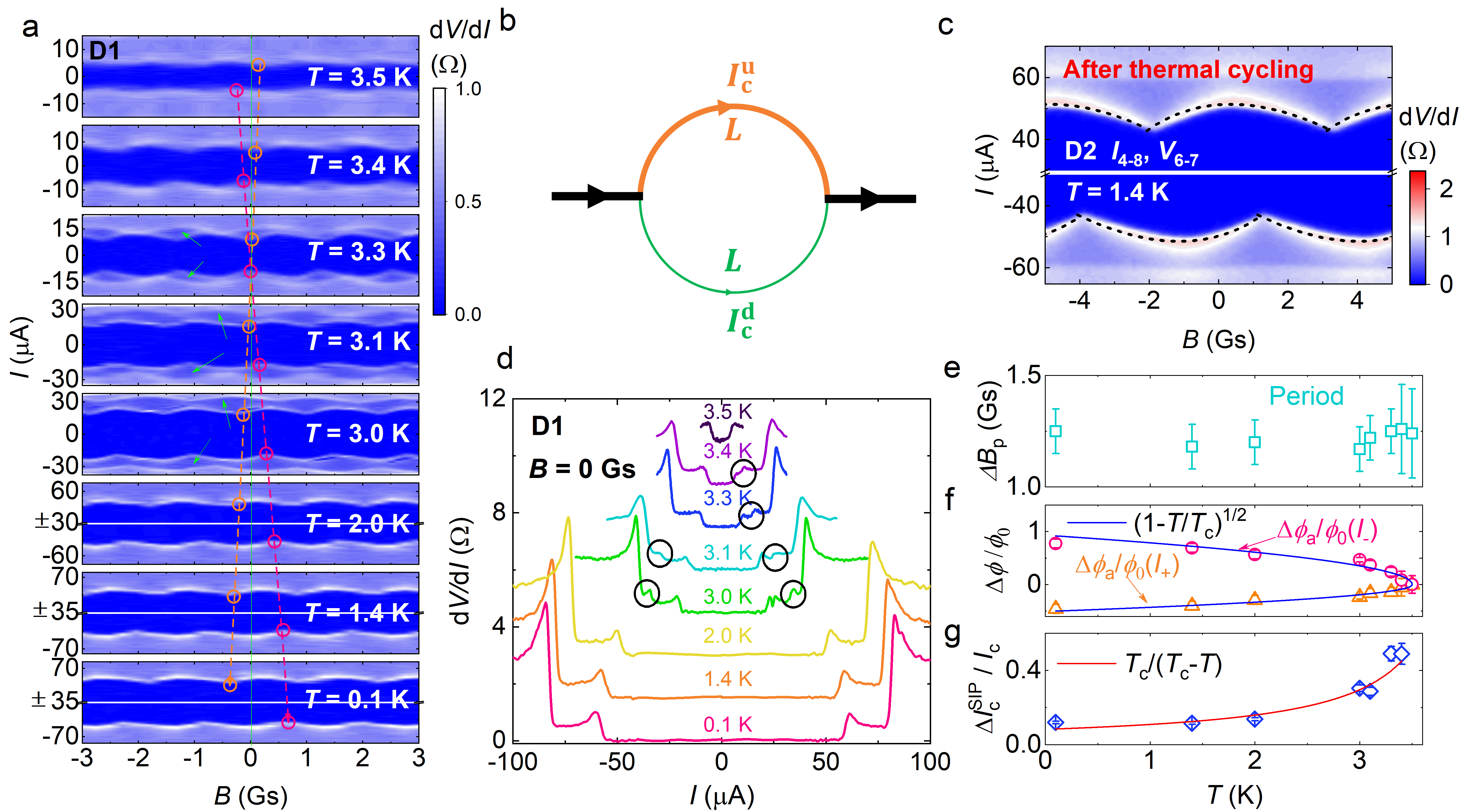
Let us now gain more insights into the SIPs by analyzing the -evolution. First, a new SIP emerges near , marked by arrows in Fig. 3a. It coincides with a sudden peak circled in the curves in Fig. 3d, implying the formation of a new supercurrent loop. This highlights domain dynamics near . Second, the period () is nearly constant within the experimental margin in Fig 3e, in contrast to the fact that diverges as approaches . This supports our argument that is truncated by the size of domains. Third, the branches of a SIP exhibit an increasingly pronounced counter-shift in phase as lowers in Fig. 3a, accounting for the SDE evolution in Fig. 1e. In Fig. 3f, the counter-shift scales as as referred from Supplementary Note 4. Finally, combining Eq. 1 and the GL theory, one deduce the oscillation amplitude , which fits our results well in Fig. 3g.
Modulation of dynamic SC domains
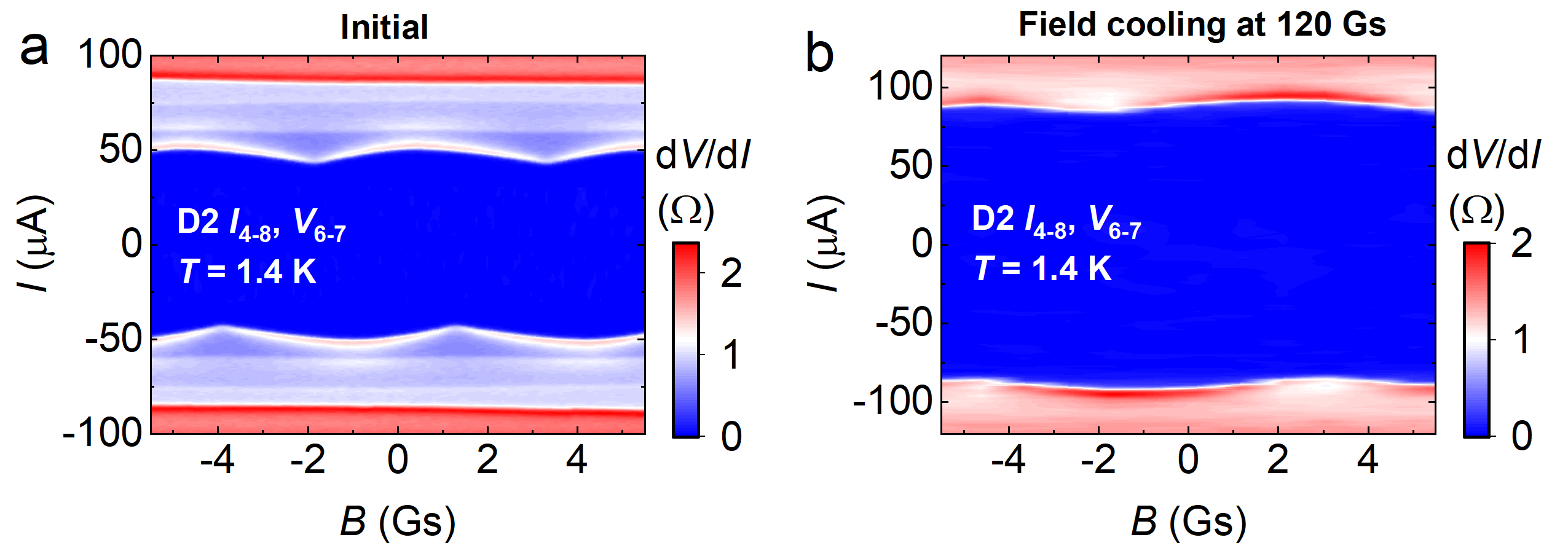
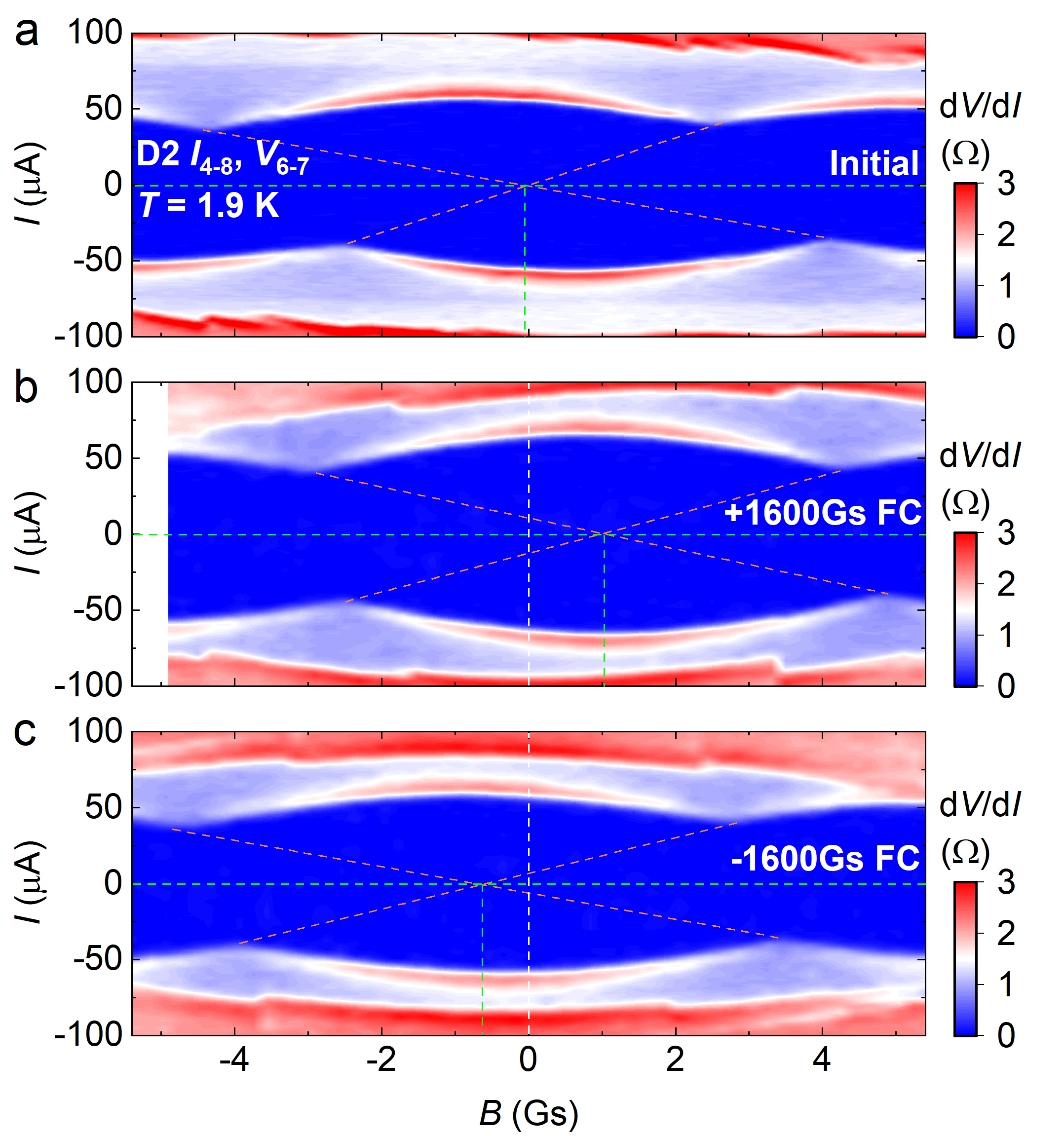
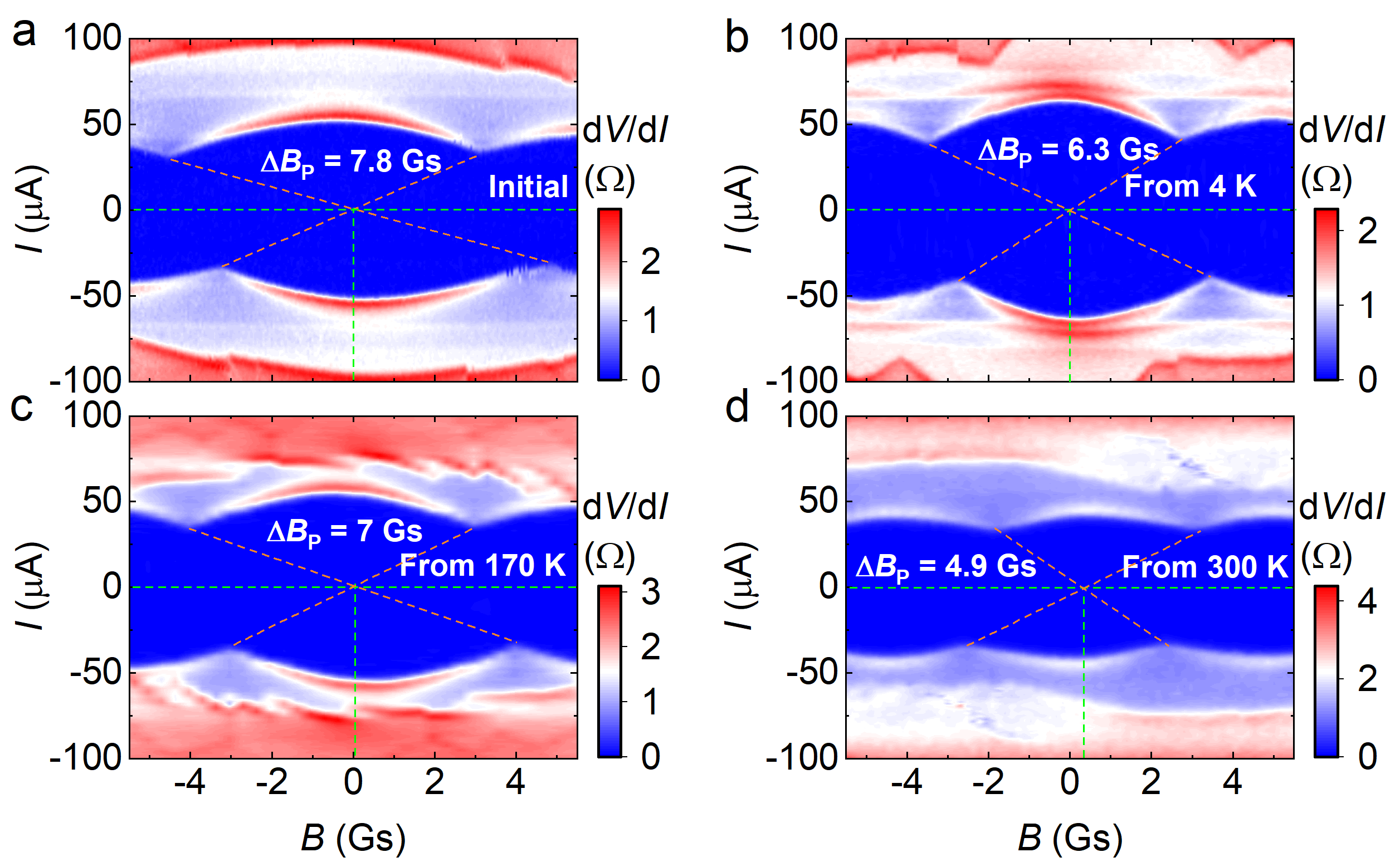
The SC domain structure is closely linked with the distribution of local defects/strains and domain dynamics influenced by thermal histories. Accordingly, we observed the SIPs are not always identical after thermal cycling, but sometimes exhibit quantitative, or even qualitative, variations. Fig. 4 shows remarkable thermal modulation of the domain size. evolves from an initial value of 7.8 Gs to 6.3 Gs after recooling the device from K, slightly above . Subsequent cooling from returns to 7 Gs. Further cooling from 300 K significantly alters to 4.9 Gs. Moreover, the patterns beyond the primary profile are substantially altered after thermal cycling. Combining Fig. 4 and Supplementary Fig. 3, 5, we also observe thermal modulation of phase and domain asymmetry. All these provide remarkable indications of the existence of dynamic SC domains. In Fig. 4b, shows noticeable changes although the thermal cycling is well below the charge ordering temperature ( K). Hence, the influence of charge order on the distribution of SC domains is not obvious. Moreover, the field modulation of SIPs is presented in Extended Data Fig. 8 and 9. They show either enhanced or “advanced” nature of hysteresis during field sweeps after field cooling, which is likely related to the rearrangement of SC domain walls driven by external 43.
Discussion
The cumulative evidence from SDEs and SIPs supports the existence of a TRS breaking SC order in CsV3Sb5. Nevertheless, the specific nature of its pairing state remains an open question. As discussed in Supplementary Note 6, previous theoretical studies have proposed a chiral pairing symmetry characterized by a full SC gap 28; 29; 30, which could reconcile our results with the majority of prior experimental outcomes 23; 24; 25; 26; 27. However, the double-degenerate orders in a SC are insufficient to form a network of chiral domains.
In the normal state of CsV3Sb5, the nematicity already disrupts the rotation symmerty of the electronic structure, transforming it into 19. There is possibility that SC developed from this state inherently possesses a nematic ground state. In this case, three types of SC domains, each accommodating two degenerate phases of opposite chirality, constitute sixfold domains, potentially responsible for the network configuration illustrated in Fig. 2g. The supercurrents flowing along domain boundaries lead to the observation of dynamic SIPs. Further details are given in Supplementary Note 7.
The method employed in this study may offer a simple probe for detecting domain edge supercurrents, contributing to the exploration of chiral SCs. The micro-sized SC domains could be further examined by high-resolution scanning probes capable of imaging current distributions. In the end, we note other scenarios, including pair-density-wave phase 11, chiral charge order 6 or significant inhomogeneity, may explain certain aspects of our findings. Their possibilities are evaluated by extended discussion in Methods. A complete understanding of all these issues still requires further efforts.
Online content
Supplementary materials are available at the online version of the paper.
References
- (1) Balents, L. Spin liquids in frustrated magnets. Nature 464, 199–208 (2010).
- (2) Ko, W.-H., Lee, P. A. & Wen, X.-G. Doped kagome system as exotic superconductor. Phys. Rev. B 79, 214502 (2009).
- (3) Zhao, H. et al. Cascade of correlated electron states in the kagome superconductor CsV3Sb5. Nature 599, 216–221 (2021).
- (4) Li, H. et al. Observation of unconventional charge density wave without acoustic phonon anomaly in kagome superconductors V3Sb5 (=Rb, Cs). Phys. Rev. X 11, 031050 (2021).
- (5) Ortiz, B. R. et al. Fermi surface mapping and the nature of charge-density-wave order in the kagome superconductor CsV3Sb5. Phys. Rev. X 11, 041030 (2021).
- (6) Mielke III, C. et al. Time-reversal symmetry-breaking charge order in a kagome superconductor. Nature 602, 245–250 (2022).
- (7) Jiang, Y.-X. et al. Unconventional chiral charge order in kagome superconductor KV3Sb5. Nat. Mater. 20, 1353–1357 (2021).
- (8) Guo, C. et al. Switchable chiral transport in charge-ordered kagome metal CsV3Sb5. Nature 611, 461–466 (2022).
- (9) Nie, L. et al. Charge-density-wave-driven electronic nematicity in a kagome superconductor. Nature 604, 59–64 (2022).
- (10) Li, H. et al. Rotation symmetry breaking in the normal state of a kagome superconductor KV3Sb5. Nat. Phys. 18, 265–270 (2022).
- (11) Chen, H. et al. Roton pair density wave in a strong-coupling kagome superconductor. Nature 599, 222–228 (2021).
- (12) Ortiz, B. R. et al. CsV3Sb5: A 2 topological kagome metal with a superconducting ground state. Phys. Rev. Lett. 125, 247002 (2020).
- (13) Ivanov, D. A. Non-Abelian statistics of half-quantum vortices in -wave superconductors. Phys. Rev. Lett. 86, 268–271 (2001).
- (14) Leggett, A. J. A theoretical description of the new phases of liquid 3He. Rev. Mod. Phys. 47, 331–414 (1975).
- (15) Kallin, C. & Berlinsky, J. Chiral superconductors. Rep. Prog. Phys. 79, 054502 (2016).
- (16) Schemm, E., Gannon, W., Wishne, C., Halperin, W. & Kapitulnik, A. Observation of broken time-reversal symmetry in the heavy-fermion superconductor UPt3. Science 345, 190–193 (2014).
- (17) Jiao, L. et al. Chiral superconductivity in heavy-fermion metal UTe2. Nature 579, 523–527 (2020).
- (18) Ming, F. et al. Evidence for chiral superconductivity on a silicon surface. Nat. Phys. 19, 500–506 (2023).
- (19) Li, H. et al. Unidirectional coherent quasiparticles in the high-temperature rotational symmetry broken phase of V3Sb5 kagome superconductors. Nat. Phys. 19, 637–642 (2023).
- (20) Zheng, L. et al. Emergent charge order in pressurized kagome superconductor CsV3Sb5. Nature 611, 682–687 (2022).
- (21) Zhao, C. et al. Nodal superconductivity and superconducting domes in the topological kagome metal CsV3Sb5. Preprint at https://arxiv.org/abs/2102.08356 (2021).
- (22) Guguchia, Z. et al. Tunable unconventional kagome superconductivity in charge ordered RbV3Sb5 and KV3Sb5. Nat. Commun. 14, 153 (2023).
- (23) Mu, C. et al. S-wave superconductivity in kagome metal CsV3Sb5 revealed by 121/123Sb NQR and 51V NMR measurements. Chin. Phys. Lett. 38, 077402 (2021).
- (24) Duan, W. et al. Nodeless superconductivity in the kagome metal CsV3Sb5. Sci. China Phys. Mechan. Astron. 64, 107462 (2021).
- (25) Roppongi, M. et al. Bulk evidence of anisotropic -wave pairing with no sign change in the kagome superconductor CsV3Sb5. Nat. Commun. 14, 667 (2023).
- (26) Zhong, Y. et al. Nodeless electron pairing in CsV3Sb5-derived kagome superconductors. Nature 617, 488–492 (2023).
- (27) Xu, H.-S. et al. Multiband superconductivity with sign-preserving order parameter in kagome superconductor CsV3Sb5. Phys. Rev. Lett. 127, 187004 (2021).
- (28) Yu, S.-L. & Li, J.-X. Chiral superconducting phase and chiral spin-density-wave phase in a Hubbard model on the kagome lattice. Phys. Rev. B 85, 144402 (2012).
- (29) Wu, X. et al. Nature of unconventional pairing in the kagome superconductors V3Sb5 (= K, Rb, Cs). Phys. Rev. Lett. 127, 177001 (2021).
- (30) Rømer, A. T., Bhattacharyya, S., Valentí, R., Christensen, M. H. & Andersen, B. M. Superconductivity from repulsive interactions on the kagome lattice. Phys. Rev. B 106, 174514 (2022).
- (31) Gupta, R. et al. Two types of charge order with distinct interplay with superconductivity in the kagome material CsV3Sb5. Commun. Phys. 5, 232 (2022).
- (32) Ando, F. et al. Observation of superconducting diode effect. Nature 584, 373–376 (2020).
- (33) Nadeem, M., Fuhrer, M. S. & Wang, X. The superconducting diode effect. Nat. Rev. Phys. 5, 558–577 (2023).
- (34) Wu, H. et al. The field-free Josephson diode in a van der Waals heterostructure. Nature 604, 653–656 (2022).
- (35) Jeon, K.-R. et al. Zero-field polarity-reversible Josephson supercurrent diodes enabled by a proximity-magnetized Pt barrier. Nat. Mater. 21, 1008–1013 (2022).
- (36) Lin, J.-X. et al. Zero-field superconducting diode effect in small-twist-angle trilayer graphene. Nat. Phys. 18, 1221–1227 (2022).
- (37) Barone, A. & Paterno, G. Physics and applications of the Josephson effect, vol. 1 (Wiley Online Library, 1982).
- (38) Wang, W. et al. Evidence for an edge supercurrent in the Weyl superconductor MoTe2. Science 368, 534–537 (2020).
- (39) Sigrist, M. & Ueda, K. Phenomenological theory of unconventional superconductivity. Rev. Mod. Phys. 63, 239–311 (1991).
- (40) Wang, D., Wang, Q.-H. & Wu, C. Symmetry constraints on direct-current Josephson diodes. Preprint at https://arxiv.org/abs/2209.12646 (2022).
- (41) Feng, X., Jiang, K., Wang, Z. & Hu, J. Chiral flux phase in the kagome superconductor V3Sb5. Sci. Bull. 66, 1384–1388 (2021).
- (42) Farhang, C., Wang, J., Ortiz, B. R., Wilson, S. D. & Xia, J. Unconventional specular optical rotation in the charge ordered state of kagome metal CsV3Sb5. Nat. Commun. 14, 5326 (2023).
-
(43)
Kidwingira, F., Strand, J.,
Van Harlingen, D. & Maeno, Y.
Dynamical superconducting order parameter domains in
Sr2RuO4.
Science 314,
1267–1271 (2006).
Methods
Growth of single crystals Single crystals of CsV3Sb5 were grown through flux methods by using Cs (purity 99.8%) bulk, V (purity 99.999%) pieces and Sb (purity 99.9999%) shot as the precursors and Cs0.4Sb0.6 as the flux agent. The starting elements were placed in an alumina crucible and sealed in a quartz ampoule in an argon-filled glove box. The ampoule was then gradually heated up to 1000 ℃ in 200 h and held at that temperature for 24 h in an oven. It was subsequently cooled down to 200 ℃ at a rate of 3.5 ℃/h. The resulting product was immersed in deionized water to remove the flux. Finally, shiny CsV3Sb5 crystals with hexagonal shape were obtained.
Fabrication of devices CsV3Sb5 nanoflakes were mechanically exfoliated from the bulk crystals using Nitto blue tape and transferred onto silicon substrates (5 mm 5 mm) capped with 300 nm SiO2. The flakes were initially spin-coated with polymethyl methacrylate (PMMA). Contacts were patterned by utilizing standard electron beam lithography (EBL) techniques (TESCAN VEGA LMS). After EBL patterning, the PMMA was immersed in a solution of methyl isobutyl ketone (MIBK)-isopropyl alcohol (IPA)(1:3) for 60 seconds, followed by rinsing with IPA. To improve the contact, the flakes were cleaned by Ar plasma, prior to deposition. Finally, the contacts with a width of 500 nm-1 m were deposited with Ti (5 nm)/Au (80 nm) via electron beam evaporation.
Resistance measurements The temperature dependence of resistance (-) for bulk and D1 from 1.8 K to 300 K was measured by standard four-terminal methods in Quantum Design physical property measurement system (PPMS). Other - curves measured around were collected in an Oxford dilution refrigerator (Triton-500).
Measurements of superconducting diode effect The zero-field superconducting diode effect was measured in Oxford dilution system (Triton-500) and Quantum Design Physical Property Measurement System (PPMS). Each measuring channel in Triton-500 was connected with a filter (QFilter-II,Qdevil), positioned at the plate of mixing chamber and to a sample-protected measurement box, located at room temperature. Prior to measurements, the flux trapped in the superconducting magnet was completely released by warming the cryostat up to room temperature. Further procedures to eliminate the environmental field is presented in Supplementary Note 1. The differential resistance (d/d) in the and regions was measured by sweeping the d.c. current bias () from 0 to or . The current bias was supplied by a current source meter (Keithley 2450). A lock-in amplifier (Stanford Research, SR830) combined with a 1 or 10 M buffer resistor was used to offer a small ac excitation current ( Hz, A A) to detect the differential resistance (d/d = /). The measurements were performed by standard four-terminal methods. For the thermal cycling measurements, two methods were employed. The first method involved heating the sample slightly above by cryostat heater and subsequently re-cooling it to the target temperature. This process is slow, usually taking more than one hour. The second method utilized a 2 k resistor, which was adhered on the SiO2/Si substrate by silver paste as a heater. The local temperature of the device was then modulated via triggering the heater with pulsed (several seconds) milliampere current applied by a current source (Keithley 6221). This process was considerably faster, taking only a few minutes.
Measurements of interference patterns The superconducting interference patterns (SIPs) were obtained by measuring d/d- curves at various fixed magnetic field () with an interval of 0.1 Gs or 0.2 Gs per trace. A current source meter (Keithley 2440 or 2400) served as the power supply for the superconducting magnet in order to achieve precise control of at sub-Gs levels. is applied along -axis, normal to the large plane of the flakes. During the measurements, the SIPs were detected within a narrow field range (e.g. -6 Gs to 6 Gs) after zero-field SDE measurements to prevent any influence from trapped vortices in samples or in the magnet, as referring to Supplementary Fig. 4. Subsequently, a higher was applied to measure the broad pattern. We observed that magnetic vortices enter into the flakes and smear the SIPs when exceeded 10 Gs, as depicted in Extended Data Fig. 5. The temperature evolution of the SIPs in Fig. 3a was detected after applying the high field. Note that 1 mA current corresponds to of 1.2 Gs in Triton-500 and 1.6 Gs in PPMS, respectively. The measurements were performed by standard four-terminal methods.
Possibility of other interpretations Before the detailed discussion, we summarize four key pieces of information from our findings:
To account for all of these findings, we have proposed the existence of domain network of chiral SC orders in Discussion and Supplementary Note 7. In the following, we will extend discussion about the possibility of other scenarios.1. Zero-field SDEs
2. Multiple transition peaks in curves
3. Well-defined double-slit SIPs
4. All the features above modulated
by thermal cycling from slighly above .
Pair density wave The pair-density-wave (PDW) phase, as revealed by scanning tunneling microscopy (STM) 11, has been theoretically proposed to be chiral 44. The potential network formed by the chiral PDW domains may account for our findings. To distinguish this possibility from chiral SC order, further investigations invoking doped or pressurized Kagome superconductors with the suppression of intricate electronic orders 20; 26 are recommended.
Significant sample inhomogeneity The bulk CsV3Sb5 single crystal is of ultra-high quality and unlikely to be inhomogeneous, as indicated in Extended Data Fig. 1. Speculation about inhomogeneity generated during device fabrication processes is reasonable. While we cannot exclude the possibility that these processes introduce some disorders, it seems unlikely that they cause significant inhomogeneity in our thick (40 nm) and highly crystalline exfoliated films. If such inhomogeneity is present, it is most likely due to sample degradation during the processes, which must be detrimental to the SC order. In contrast, is increased by about 20% in our devices, similar to the previous report 45. Ref. 45 reported a systematic evolution of with counter-evolution of as the device thickness reduces. This phenomenon cannot be reconciled with the generation of significant inhomogeneity. However, if substantial inhomogeneity exists in the device, it will result in discrete islands of SC order with varying connected by weak links. In this case, the SC islands are asymmetric and in series, this could lead to zero-field SDE and multiple transition peaks given that TRS is broken, e.g. from the chiral charge order. The supercurrent across weak links may also induce Fraunhofer-like SIPs. But this is difficult to reconcile with the observation of the sharp double-slit SIPs. Additionally, such inhomogeneity is usually static, which fails to explain the thermal modulation near .
Chiral charge order The chiral charge order ( K) breaks TRS in the normal state. Combined with the IRS breaking, e.g. geometric asymmetry, it potentially gives rise to zero-field SDEs, but it hardly accounts for the other three items. Subsequent concern involves the possible existence of chiral charge order domains with normal state edge currents. Their fate in the SC state is still unknown. Assuming that it persists into the SC state with the domain boundaries remaining normal, these boundaries could act as weak links cutting a homogeneous SC phase into pieces. The asymmetry of the domain and spatial variation in link strength may contribute to zero-filed SDEs and multiple transition peaks. The supercurrent across weak links may induce Fraunhofer-like SIPs, however this is challenging to account for the distinct double-slit SIPs in the absence of edge supercurrent. Additionally, the charge order is usually static near , which fails to explain the dynamic properties. In short, the charge order domain scenario could potentially account for terms 1 and 2 under substantial assumptions, it faces challenges in elucidating terms 3 and 4.
Composite domain network The scenarios discussed above struggle to explain the crucial information of our results (terms 3 and 4). The distinct features of the sharp double-slit SIPs are usually associated with closed edge supercurrents and their dynamic properties are highly correlated with the SC transition. An intuitive explanation for these phenomena lies in the emergence of chiral SC domains. We have explained that a two-component chiral SC order parameter (e.g. ) alone is insufficient to generate a domain network, the formation of which requires the additional presence of rotation symmetry breaking from to symmetry in CsV3Sb5. Below, we propose an alternative scenario involving a composite domain network, where the two-component SC domains emerge on top of multiple SC regions already separated by weak links from, for instance, significant inhomogeneity. Though the likelihood of this scenario is minimal, it could potentially offer an additional explanation for our observations.
Data availability Data are available from the corresponding author upon reasonable request.
- (44) Zhou, S. & Wang, Z. Chern Fermi pocket, topological pair density wave, and charge-4 and charge-6 superconductivity in kagomé superconductors. Nat. Commun. 13, 7288 (2022).
- (45) Song, B. et al. Anomalous enhancement of charge density wave in kagome superconductor CsV3Sb5 approaching the 2D limit. Nat. Commun. 14, 2492 (2023).
- (46) Liang, Z. et al. Three-dimensional charge density wave and surface-dependent vortex-core states in a kagome superconductor CsV3Sb5. Phys. Rev. X 11, 031026 (2021).
- (47) Fu, Y. et al. Quantum transport evidence of topological band structures of kagome superconductor CsV3Sb5. Phys. Rev. Lett. 127, 207002 (2021).
Acknowledgments The authors are grateful to Lin Jiao and Chunyu Guo for the helpful discussion. This research is supported by Zhejiang Provincial Natural Science Foundation of China for Distinguished Young Scholars under Grant No. LR23A040001. C.W. is supported by the National Natural Science Foundation of China under the Grants No. 12234016 and No. 12174317. T.L. acknowledges support from the China Postdoctoral Science Foundation (Grant No. 2022M722845 and No. 2023T160586). This work has been supported by the New Cornerstone Science Foundation. X.L. acknowledges the support by the Research Center for Industries of the Future (RCIF) at Westlake University under Award No. WU2023C009. The authors thank the support provided by Dr. Chao Zhang from Instrumentation and Service Center for Physical Sciences at Westlake University.
Author contributions T.L. fabricated the devices and did the transport measurements assisted by Z.X., J.W., Z.L. and X.Y.. J.L. prepared the samples supervised by Z.W. and Y.Y.. Z.P. did theoretical calculations supervised by C.W.. T.L., Z.P. and X.L. prepared the figures. X.L. wrote the paper with the inputs from T.L., Z.P. and C.W.. X.L. led the project. All authors contributed to the discussion.
Competing interests The authors declare no competing interests.
Additional information
Supplementary information are available at the online version of the paper.
Correspondence and requests for materials should be addressed to Zhiwei Wang, Congjun Wu or Xiao Lin.