Structural, mechanical, and electronic properties of single graphyne layers based on a 2D biphenylene network
Abstract
Graphene is a promising material for the development of applications in nanoelectronic devices, but the lack of a band gap necessitates the search for ways to tune its electronic properties. In addition to doping, defects, and nanoribbons, a more radical alternative is the development of 2D forms with structures that are in clear departure from the honeycomb lattice, such as graphynes, with the distinctive property of involving carbon atoms with both hybridizations and . The density and details of how the acetylenic links are distributed allow for a variety of electronic signatures. Here we propose a graphyne system based on the recently synthesized biphenylene monolayer. We demonstrate that this system features highly localized states with a spin-polarized semiconducting configuration. We study its stability and show that the system’s structural details directly influence its highly anisotropic electronic properties. Finally, we show that the symmetry of the frontier states can be further tuned by modulating the size of the acetylenic chains forming the system.
I Introduction
The nanoscale systems studied in the literature comprise a large number of structures with several different chemical compositions and structural arrangements song2010 ; lin2013 ; bianco2013 ; geim2013 ; das2014 ; algara2014 ; zhu2015 . Carbon-based nanostructures are key examples of such materials for historical and scientific reasons. On the one hand, the development timeline of this research field is closely related to nanocarbon forms such as fullerenes, nanotubes, and graphene noorden2011 . On the other hand, carbon nanostructures have physical and chemical properties that can be modulated over a wide range of possibilities due to the details of their atomic structures dai2002 ; jia2011 ; terrones2012 ; meunier2016 .
Today, graphene is the most iconic representative of the nanocarbon family. However, many forms based on chemical and/or physical modifications of graphene have been studied as motivated by the need to open an electronic band gap, absent in pristine graphene. These include, but are not limited to, doping cruzsilva2011 ; lee2018 , insertion of defects amorim2007 ; botello2011 , and cutting in nanoribbon samples son2006 ; son2006b ; pisani2007 . Another perspective is to investigate different ways to organize carbon in two-dimensional lattices different from graphene’s girao2023 . These alternative nanocarbon allotropes are commonly proposed by theory terrones2000 ; Mathew2010 , but some representatives have also been successfully synthesized, such as 2D biphenylene (BPN) Qitang2021 . Most of these systems are based on carbon hybridization, where carbon atoms bind to three atomic sites. However, the study of carbon at the nanoscale has also been pushed into setups involving other hybridizations. These include, for example, systems with a mixture of and atoms, with pentagraphene zhang2015 , tetrahexcarbon ram2018 , and ph-graphene zhang2016 as notable examples. Graphynes make up another class of systems that have been studied well before these materials baughman1987 . Graphyne (GY) is a one-atom-thick layer where and hybridized carbon atoms coexist. They have been investigated in many structural variations through theoretical calculations, with -, -, and -GY among the best-known examples Kang2011 ; Malko2012 ; Wu2013 . In structural terms, GY structures are usually defined from graphene as a starting point and differ from each other by different distributions and concentrations of acetylenic units (), as well as by the length of these connections ivanovskii2013 ; Wu2013 ; Kang2019 . The science of GYs has also gained more relevance after the synthesis of graphydiine li2010 and a TP-GDY analog featuring a triphenylene structural unit Matsuoka2019a . Recent literature has witnessed the theoretical proposal of GY forms not inspired by the graphene lattice but featuring other rings such as tetragons, pentagons, heptagons, etc. yin2013 ; Nulakani2017 ; Wang2019 ; oliveira2022 .
The proposal of new 2D nanocarbon forms, the investigation of non-graphitic GY systems, and the experimental realization of 2D byphenylene and some GY forms lead us to propose and study a GY structure based on the 2D BPN lattice. The GY we consider here is based on including a minimal acetylenic sector sandwiched between each pair of first-nearest-neighbor carbon atoms from BPN. We use density functional theory simulations to gain insight into the stability of this system and investigate its electronic structure. We demonstrate that this system preserves spin-based electronic states that were previously reported in the BPN counterpart alcon2022 . However, the spin-polarized state results in a semiconducting configuration, resulting in a system with high potential for applications in nanoelectronics and spintronics.
II Methods
Our computational simulations are based on density functional theory (DFT) hohenberg1964 ; kohn1965 implemented in the SIESTA code Soler2002 . Core electrons are considered by employing Troullier-Martins pseudopotentials troullier1991 and valence electrons are described in terms of a double- polarized (DZP) basis set of numerical atomic orbitals Soler2002 . The exchange-correlation energy is taken into account using the generalized gradient approximation (GGA) as parameterized by Perdew-Burke-Ernzerhof (PBE) perdew1996 . Real-space integrations are performed on a grid defined by a 400 Ry mesh cutoff, and a Monkhorst-Pack sampling is used for reciprocal space integrations for the studied GY nanosheets. We consider -sampling schemes with a similar density of -points for other systems considered in this study. During optimization of the atomic structures for the calculation of electronic properties, no constraints were imposed. We considered a maximum post-relaxation force of 0.01 eV/Å for each atom and a maximum 0.1 GPa tolerance for stress components while optimizing the lattice parameters. We also performed Born-Oppenheimer molecular dynamics (BO-MD) simulations within SIESTA using an NVT (canonical) ensemble and a Nosé thermostat.
Phonon band structure calculations were performed with the DFT-based GPAW code mortensen2005 ; enkovaara2010 . We used the finite difference method with atomic displacements of 0.01 Å to calculate force constants together with the PHONOPY package togo2015 . GPAW uses the grid-based projector-augmented wave (PAW) method in the description of electron-ion interactions blochl1994 . For manipulation and analysis of atomic simulations, GPAW uses the atomic simulation environment (ASE) package larsen2017 . The GGA-PBE functional was also considered in the GPAW simulations. A 500 eV energy cutoff was adopted to define the plane-wave basis, and a 0.1 eV smearing was used to compute Fermi-Dirac occupations. The supercell considered in these simulations was sampled with Monkhorst–Pack points for reciprocal space integrations. The quasi-Newton method is used for atomic coordinate optimization considering a maximum threshold value of 1 meV/Å for atomic forces and 0.01 GPa for stress, with the structures further symmetrized with PHONOPY.
III Results and Discussion
III.1 Structural details
Fig. 1a illustrates the BPN structure, with the primitive unit cell highlighted by a red rectangle. Its lattice parameters, and (red arrows), the two non-equivalent (blue circle) and (pink circle) atoms in the structure, and its four different bond types (green segments) are also illustrated in Fig. 1a. The types of bonds are denoted by , , , and , depending on the atoms involved in each bond. In that case, represents the bond length between two atoms inside the same hexagon, while represents a bond between two atoms from different hexagons. These bond lengths have the following values: Å, Å, Å, and Å. This system is organized in a rectangular 2D Bravais lattice, with vectors and along the and directions, respectively. These BPN lattice parameters are Å and Å.
Fig. 1b illustrates the -GY structure based on the BPN lattice, or simply -BPNGY. It consists of the insertion of a minimal acetylenic chain () in the middle of each and all of the original links from BPN. The -BPNGY monolayer has lattice parameters Å and Å, with nearly the same aspect ratio () compared to BPN (). For the -BPNGY bond lengths, we have one and two bonds corresponding to each connection from BPN. First, we look at the -BPNGY bridges analogous to the , , and links in BPN. By symmetry, the two bonds in each of these bridges are equivalent. We find 1.411 Å, 1.401 Å, and 1.420 Å values for such bonds in the , , and -BPNGY bridges, respectively. The corresponding values for the links are very similar to each other, namely 1.399 Å and 1.393 Å. We note that these values are within a range between 1.393 Å and 1.420 Å, which is narrower than the corresponding range of bonds in BPN (from 1.412 Å to 1.461 Å). For the bonds along the , , , and links, we find 1.236 Å, 1.245 Å, 1.237 Å, and 1.244 Å, respectively, a range narrower than in the cases. This is similar to what happens in other non-graphitic GY structures oliveira2022 ; vieira2024 and reflects the fact that the non-hexagonal rings are better accommodated in GY structures than in their full- counterparts due to the large rings structure. All these bond lengths are listed in Table 1.
| Bond type | bond length (NP) | bond length (NP) |
|---|---|---|
| () | 1.411 Å | 1.410 Å |
| () | 1.399/1.393 Å | 1.400/1.393 Å |
| () | 1.401 Å | 1.405 Å |
| () | 1.420 Å | 1.416 Å |
| () | 1.236 Å | 1.236 Å |
| () | 1.244 Å | 1.244 Å |
| () | 1.245 Å | 1.243 Å |
| () | 1.237 Å | 1.238 Å |
The bond-angle profiles also illustrate the better accommodation of non-hexagonal rings in GY structures, especially for the 4-membered rings. In BPN, the internal angles from the tetragonal rings are . This results in a local structure with strong electronic repulsion between the charge density clouds of the orthogonal bonds emerging from a given site, and it is likely to be the most reactive sector of the structure. In -BPNGY, due to a better accommodation of the interatomic bonds, the internal angles of the 4-membered cycles at the sites are , much closer to the angle from the corresponding “perfect” hybridization in graphene, similar to other BPN-based GY recently proposed vieira2024 . Overall, all the atoms in -BPNGY have a bond angle profile closer to that of carbon atoms in graphene, compared to BPN. This is illustrated in Fig. 1c-d for BPN and -BPNGY, respectively, with the color scale indicated in Fig. 1e. To accommodate angles closer to the characteristic value found for hybridization, the bridges that make up the tetragonal rings are curved outward of the ring, while those bridges that link successive hexagons along the direction maintain their linear configuration.

III.2 Stability of -BPNGY
To evaluate the stability of -BPNGY relative to other known systems, we computed the formation energy per atom. Here, we define this energy in two different ways. First, we considered the ) parameter defined as
| (1) |
where () is the total energy of the system (number of atoms) per unit cell, and represents the energy per atom in graphene. In simple terms, compares the energy per atom in the system with the energy per atom in graphene, used as reference. We computed for -BPNGY, the conventional graphene-like -, -, and -GYs, graphene, BPN, and a polyyne chain, with the corresponding values listed in Table 2 in ascending order. Taking into account the definition of Eq. 1, for graphene is set as zero as a reference, as it is the most stable system considered here. From the data in Table 2, BPN is found to be the most stable system in the list after graphene. Except for a polyyne chain, -BPNGY is the less stable system.
It is important to note that the computation of considers carbon atoms and on the same footing compared to the energy per atom in graphene. One should note that the and states of carbon represent two stable hybridization states and occur spontaneously in nature. However, even though their relative stabilities are expected to be different from each other, there is a thermodynamic barrier that prevents a transition from occurring freely. For this reason, we compared the energy of the system, taking into account its composition, with that of separate and reference systems. Therefore, we defined a second quantity as
| (2) |
where () is the number of atoms with () hybridization and () is the energy per atom in a polyyne chain (graphene). So, for the and (polyyne chain and graphene) is set to zero as the reference system. Note that this gives a contrasted view of relative formation energies. For instance, graphene is now on the same comparison level as a polyyne chain (which was considered the less stable system according to ). The corresponding data for is also listed in Table 2 in ascending order. From this metric, we conclude that -BPNGY is much closer to its pair of reference systems than BPN, as is equal to 0.200 eV and 0.483 eV for -BPNGY and BPN, respectively. When compared to the traditional GY systems, -BPNGY is found to be slightly less stable than them, considering both and .
| System | (eV) | System | (eV) |
| Graphene | 0.000 | Graphene | 0.000 |
| BPN | 0.483 | Polyyne | 0.000 |
| -GY | 0.752 | -GY | 0.107 |
| -GY | 1.009 | -GY | 0.149 |
| -GY | 1.129 | -GY | 0.162 |
| -BPNGY | 1.167 | -BPNGY | 0.200 |
| Polyyne | 1.289 | BPN | 0.483 |
Dynamical stability, as evaluated from the phonon band structure, is also important to consider when suggesting whether a system is likely to be synthesized. We show the phonons band structure of -BPNGY in Fig. 2a, where we observe no imaginary modes (which would conventionally appear as negative frequencies), indicating that the system is dynamically stable. The phonon dispersion of -BPNGY lacks a gap between the acoustic and optical modes. This phenomenon is commonly associated with systems that exhibit low thermal conductivity, a typical feature of materials containing acetylenic groups (graphyne-type systems), due to elevated phonon scattering within the system santos2024proposing ; mortazavi2022ultrahigh ; wang2016tunable . Another characteristic commonly observed in graphyne systems is the presence of a flat dispersion band around 66 THz, which is also evident in -BPNGY. This phonon mode is related to the vibrations of the sp bonds in the acetylenic groups jenkins2024thd , which are inserted between the and atoms in BPN (see Fig. 1a). In addition to a flat dispersion, the range of isolated frequencies between 55 and 66 THz is directly related to the transition from BPN to -BPNGY, with the system showing a maximum dispersion beyond this isolated range, around 45 THz, which is close to that observed in the biphenylene network luo2021first .

We can also assess thermal stability using BO-MD simulations. Here we considered a supercell, a total simulation time of 3 ps (with a timestep of 0.5 fs), and a temperature value of 400 K. During the entire simulated dynamics, no bond breaking or formation was observed from a visual inspection of the trajectory. Beyond visual inspection of the animation, a quantitative way to evaluate the integrity of the system is the computation of the Lindemann indices: its local (, ranging over the structure’s atoms) and global () values ding2005 ; singh2013 . The maximum values for and were less than 0.0281, which is a good indication of the integrity of the system if we compare it with other nanocarbon systems zhang2007 ; silva2020 ; oliveira2022 . In Fig. 2b, we also show the total energy per atom as a function of time for the BO-MD simulation. Apart from characteristic fluctuations of MD simulations, we observe no abrupt changes in the energy profile, indicating the absence of structural transitions during the time evolution.
We note that neither the phonon analysis nor the molecular dynamics results take into account variations in the lattice parameters of the system. This aspect is the basis for the definition of the system’s elastic tensor components: , , , and , corresponding to , , according to the Voigt notation andrew2012 . These quantities allow us to compute the elastic strain energy , defined as the difference between the total energy of the strained and relaxed systems per unit area. The relation between and the s components is written for low-strain values as:
| (3) |
Here, () is the strain component along the () direction, while represents shear stress. Considering that the lattice vectors of the relaxed system are given by
| (4) |
the and strain values are defined as:
| (5) |
with () being the relaxed lattice constant along () and () the corresponding strained values. The and cases correspond to a uniaxial strain applied along and , respectively. Biaxial strain corresponds to the case. The application of shear strain corresponds to the following strained vectors major2013
| (6) |
We considered the strain values -0.01, -0.005, 0.000, 0.005 and 0.01 applied separately for uniaxial strain along and , biaxial and shear strains. In the following, we used the corresponding versus relations to obtain the elastic tensor components through least-square fitting. The resulting values are N/m, N/m, N/m, and N/m. These values obey the Born-Huang criteria born1954 ; ding2013 ; zhang2015 , and , predicting -BPNGY as a mechanically stable material.
III.3 Mechanical Properties
We now compare these results regarding the elastic constants of -BPNGY with those of a BPN layer, for which we obtained N/m, N/m, N/m, and N/m through the same procedure applied to -BPNGY. In general, the elastic tensor components for the graphynic system are significantly smaller than for the full- system, as -BPNGY has long acetylenic chains and a less dense structure, giving it a particularly higher flexible character compared to BPN. Regarding anisotropy, -BPNGY, and BPN are fairly similar, since for BPN and for the graphynic system. On the other hand, the -BPNGY value is much smaller compared to the other components of the system and to the corresponding value for BPN. It turns out that the unit cell area in shear strain varies within a much smaller range compared to uniaxial and biaxial strain. Together with the high porosity and flexibility of -BPNGY, this explains the very small value for the GY system.
In addition to the previous discussion on stability and anisotropy, the elastic tensor also allows us to determine the mechanical response of -BPNGY and that of the fully sp2 system for comparison. From this perspective, we can obtain the Young’s modulus and Poisson’s ratio through the following relations cadelano2010 :
| (7) |
and
| (8) |
where , and denotes the in-plane direction relative to the axis.
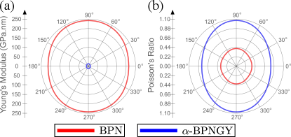
Fig. 3a (Fig. 3b) plots () as a function of the in-plane direction (in terms of the angle relative to the axis) for -BPNGY (blue line) and the BPN sheet (red line). For the fully system, the material exhibits slight anisotropy, with ranging from 213.7 N/m to 242.5 N/m for (same for ) and (same for ), respectively. Considering the thickness of graphene, equal to 0.335 nm shearer2016accurate , this corresponds to a variation from 638 GPa to 724 GPa in the and directions, respectively, which are lower values than graphene’s sakhaee2009elastic . Since BPN is composed of three different carbon rings, two of which are nearly regular (hexagon and tetragon), the octagonal ring exhibits an irregular characteristic with its longitudinal direction parallel to the direction of the system (see Fig. 1), making BPN stiffer in this direction. Applying tension along the direction compresses the octagonal ring further, compared to tension in the direction, which leads to the expansion of the 8-membered ring. This same geometric aspect of the system explains the Poisson’s ratio of BPN, which varies from approximately to for (same for ) and (same for ), respectively. Similarly to the discussion on Young’s modulus, the octagonal ring plays a crucial role in the expansion/compression of the nanomaterial, depending on whether the external force is applied parallel or perpendicular to the longitudinal direction of the octagonal carbon ring. Regardless of the direction of tension, indicates that BPN is a ductile system, and even though reaches about 70% of the value reported for graphene, it differs in terms of brittleness wang2019dhq ; zhang2015fracture . It is important to note that this ductile behavior has already been reported for BPN based on fully atomistic simulations, which considered temperature effects and larger-scale systems pereira2022mechanical .
For -BPNGY, the Young’s modulus is generally significantly lower for the graphyne case, while the Poisson ratio is more pronounced. This result is expected for a graphyne-type system. As discussed and shown in Fig. 1, the structural degrees of freedom in graphyne-type systems tend to bring the hybridizations of the nanomaterial closer to their ideal values, forming angles of . When tension is applied, the energy associated with angle formation is much lower than that associated with and bonds, making the angles easily adjustable under external pressure, making -BPNGY a more malleable system. Consequently, this reduces the value of , which ranges from 10.1 N/m, in the direction, to 13.3 N/m, in the direction. Taking into account the graphene’s thickness, these values correspond to 30.1 GPa and 39.7 GPa, respectively, which are close to the values reported for -GY, i.e., approximately 30.2 GPa in both directions zhang2014graphene . On the other hand, varies from 0.80 to 1.07 in the and directions, respectively. Thus, -BPNGY is considerably more ductile than BPN, given the ease of angle rearrangement in graphyne systems, which facilitates geometric changes when tension is applied. These differences have been reported for other graphyne systems based on two-dimensional materials with and hybridization zhang2015penta ; deb2020pentagraphyne ; de2023nanomechanical ; peng2014new ; vieira2024electronic .
III.4 Electronic properties
In terms of electronic properties, we first revisit the electronic structure of the BPN layer so we can compare it with the properties of the GY structure. We initially did not explicitly consider the spin degree of freedom. This spin-paired electronic configuration will be referred to as an NP (non-polarized) state and its corresponding band structure, evaluated along high-symmetry lines of the Brillouin zone (BZ), is shown in Fig. 4a together with the corresponding density of states (DOS). The plots confirm the metallic behavior of BPN previously reported in theoretical Mathew2010 ; bafekry2022 and experimental Qitang2021 studies. We observe bands crossing the Fermi level along all the high-symmetry lines, except for the path. We will pay special attention to the frontier bands indicated by labels I and II in Fig. 4a. We plot these two bands over the entire Brillouin zone in Fig. 4b, with the Fermi level represented by the green rectangle. From these plots, we verify that bands I and II intercept each other by forming a pair of cone-shaped crossings along the path, at an energy eV above the Fermi level. Along the path, band I forms a low-dispersive branch (highlighted by a red dashed ellipse in Fig. 4a) associated with a narrow energy range of high DOS values. The bottom of this sector is also indicated by (i) in Fig. 4a. In the bands plot shown in Fig. 4a, we also note a slightly more dispersive branch crossing along the path (highlighted by a blue dashed ellipse in Fig. 4a). The top of this band results in a DOS peak and is indicated by the label (ii) in Fig. 4a. We plot the local DOS (LDOS) for the energy points (i) and (ii) in Fig. 4c. These levels are strongly associated with the BPN squares. It turns out that the angles between the edges of these rings result in a region with a high electronic density due to the proximity of the electronic charges involved in these chemical bonds. The strong electronic repulsion originating from this sector is responsible for bringing electronic states close to the Fermi level of the system, as indicated by the plots in Figs. 4a-c.

Furthermore, band I (II) also has a minimum (maximum) value at the () point of the BZ. The maximum (minimum) energy value of band II (I) at the () point is also indicated by the (iii) ((iv)) label in Fig. 4a. These energy value extrema do not result in DOS peaks, but they will be relevant when compared with the BPNGY systems. For this reason, we plot their LDOS in Fig. 4c. These states are distributed over the entire structure and are not particularly limited to the squares. To gain more insight into the (iii) and (iv) states, we plot the real part of their corresponding wave-functions in Fig. 4d. The cyan/yellow colors indicate opposite signs for the wave-function amplitudes. Focusing on the hexagons in the (iii) state, we find that the wave-function phase is inverted as we move from one ring to the neighboring one along the direction. This is consistent with the position of this state in the Brillouin zone because the point is given by
| (9) |
and since , its corresponding Bloch phase for the displacement is
| (10) |
We note that the phase is the same when moving between two neighboring hexagons along the direction () since
| (11) |
In the case of the (iv) state, the wave-function sign is inverted both when moving between adjacent hexagons along the and directions, since
| (12) |
and
| (13) |
for both and .
2D BPN is composed solely of even-membered rings, namely tetragons, hexagons, and octagons. Because of this, one expects BPN to be a bipartite lattice. This means that its atoms can be split into two sets, A and B, so that all the first nearest-neighbors to any A atom come from the B set, and vice versa. However, if we label the atoms according to the A and B sets, we end up breaking the bipartition at the edges of the primitive cell, since we necessarily find A-A and B-B bonds. To fully accommodate bipartition in the periodic BPN structure, one has to necessarily consider a conventional supercell containing 12 atoms, as represented in Fig. 4e. This is because the A/B designations in neighboring hexagons along the direction have to be swapped to obey the bipartite organization, which justifies the need for a conventional cell with two hexagons. This cell has lattice parameters given by Å and Å, with the second one being twice the value of the corresponding one in the primitive cell. The corresponding unit cell in the reciprocal space will have half the size of the original BZ along the direction, as represented in Fig. 4f. This is the reason why we expect doubly-degenerated bands along the path for calculations involving the conventional cell. Although the electronic properties in the NP state should not be affected in a calculation based on the conventional cell, such a setup will allow the electronic charge to converge to a different configuration in a spin-polarized calculation alcon2022 .
Fig. 4h shows the electronic band structure of BPN in the NP state considering the doubled cell. These bands are consistent with the bands obtained in the calculation using the primitive cell (Fig. 4a). As discussed above, the bands shown in Fig. 4h are degenerated two-by-two along the new path for the NP BPN sheet. In Fig. 4h we also plot the BPN’s frontier bands over the entire BZ for this conventional cell setup, where we note that the states around the point in the primitive cell setup are now moved to lie in another -path around the new point of the BZ.
In the following, we show the electronic band structure of spin-polarized (SP) BPN along the high-symmetry lines of the BZ in Fig. 4i, with the corresponding DOS plot. We also show the valence and conduction bands over the entire BZ with surface plots in Fig. 4i. We first note that even though this is a spin-polarized state, the corresponding bands are spin-degenerated. This is understood in terms of the difference between the spin-up and -down components of the electronic density, represented in Fig. 4g, with blue (red) clouds representing excess spin-up (-down) charges. We note this is a configuration with zero total magnetic moment, and there is a symmetry between the spin components of the electronic charge (consistent with the lattice bipartition). This agrees with Lieb’s theorem lieb1989 , as the number of atoms is the same in the two sublattices composing the BPN structure yazyev2010 . One notes that the spin-up and -down densities can be swapped by mirror symmetry operations along the crystallographic directions. We highlight that this SP configuration in BPN is not accompanied by any Peierls-like distortion of the atomic structure. In other words, each of the two unit cells composing the double supercell has the same bond-length and bond-angle structure as that obtained from a primitive cell-based calculation. In this sense, we conclude the use of the primitive cell leads to a magnetically frustrated (NP) configuration. On the other hand, the doubled supercell allows extra degrees of freedom, resulting in a broader set of hypothetical magnetic configurations to test. This includes the SP case discussed here and in previous literature alcon2022 , which turns out to be the system’s ground state. But here, the frustration mechanism is driven by the accommodation of the lattice bipartition only in the double supercell, rather than by lattice distortion hou2015 or defects/temperature effects bayaraa2021 ; kundu2023 as observed in other materials.
In addition, the band structure for this SP state is very similar to that of the NP case. The most remarkable change in the band structure for SP relative to the NP configuration is the opening of the bands crossing close to the along the path. This opening is followed by the other states along the -curves around the point where the NP system has bands crossing the (as seen by comparing Fig. 4h-i). This band anti-crossing in the SP configuration collapses into the pair of cones symmetrically located along the path, with the additional effect that these cones are now moved to the Fermi level. This is also manifest in the DOS plot for the SP state, which features a zero-gap signature at resulting from this cone-like intersection between the valence and conduction bands of the SP BPN system.

Moving to the -BPNGY layer, Fig. 5a shows its electronic band structure, which reveals that this system is metallic. Here, the spin-degree of freedom is not considered explicitly in this NP configuration. A notable feature of -BPNGY’s electronic structure is the presence of a pair of flat sectors from two bands close to the Fermi level (), a feature shared with another BPNGY system vieira2024 . These localized branches resemble the BPN less dispersive branches marked by red and blue dashed ellipses in Fig. 4a. One of these flat bands lies 0.04 eV above along the path, and the other 0.03 eV below the Fermi level along the line. These bands are marked as I and II in Fig. 5a, respectively. The band II is the one that crosses the , around the point in -space, where it has its minimum. These features can be easily seen from a surface plot of the I and II bands over the entire BZ in Fig. 5c. The flat bands result in two prominent peaks (P1 and P2) in the DOS plot of the structure, presented in Fig. 5b. The DOS also features two peaks around -0.50 and +0.46 eV, which are related to the saddle-like regions of bands I and II, respectively (as indicated by red circles in Fig. 5c). We also plot the LDOS for the two flat states of branches I and II in Figs. 5d,e, respectively. We observe that these states are distributed mainly over the atoms of the tetragonal rings, similar to the states in BPN. However, the electronic charge density shown in the two plots of Figs. 5d,e involve complementary sets of bonds. Namely, P1 is mostly distributed over the bonds of the bridges shared by tetragonal and octagonal rings, and over the bonds of the bridges shared by tetragonal and hexagonal rings. On the other hand, P2 extends over the bonds of the bridges between the tetragonal and octagonal rings, and over the bonds of the links between the tetragonal and hexagonal cycles. In addition, the flat states (P1 and P2) also spread over the other four atoms of the hexagonal rings that do not belong to the tetragonal rings. These states show a negligible amplitude over the acetylenic bonds linking successive hexagons along the direction. As a result, these levels look like quasi-1D states along the direction. This is similar to the behavior of the frontier states of naphthylene- (-graphene) beserra2020 , as well as to a BPNGY counterpart vieira2024 . The weak participation of the sectors linking successive hexagons along the direction compared to their counterparts in the tetragonal and hexagonal rings can be rationalized in terms of the structural details shown in Fig. 1d. The bridges that form the tetragon and hexagon sectors are curved, bringing their corresponding levels close to the . On the other hand, the bridges between hexagons are more stable sectors due to their perfectly linear configuration.
Another notable aspect is that the I and II bands of -BPNGY present a minimum at and a maximum at , respectively. This is similar to the BPN case, but inverted. That is, band II has a maximum at , and band I has a minimum at . Such inversion behavior for the bands along the energy axis has also been reported for other graphynic systems relative to their full- counterparts oliveira2022 ; vieira2024 . Although these effects are not easily rationalized from the complexity of the calculation, we can examine a number of features of specific states that are consistent with the inversion. As we did for BPN, we plot the wave-functions for the minimum of I at and for the maximum of II at in Figs. 5f-g, respectively. From a chemistry point of view, these states alternate between bonding (nonzero wave-function spreading over the bond between two atoms) and anti-bonding (a wave-function node in the middle of the bond between two atoms) characters over the structure. The bonding character is even more explicit for the minimum of I at , as it spreads over trimers (at the corners of the hexagonal rings). So, it is natural to expect that state I at has a lower energy value compared to state II at . Note the wave-function of the I minimum at is odd for successive hexagonal rings along the direction, and even along the direction. This is consistent with the position of the point in the BZ and similar to the (iii) state in BPN (see Fig. 4a). In this way, the six atoms of a given hexagonal ring have alternating phases for the wave-function. In addition, due to the bonding character of the wave-function lobes, the dimer between two of these atoms cannot form a bonding pattern, otherwise, the two atoms would have the same phase (opposite to the central dimer), breaking the state’s symmetry. Instead, the atoms of the acetylenic dimer in the hexagon form nodal planes in their middle sector and bond lobes with the sites, as shown in Fig. 5f. The stronger bonding character of state I at compared to the wave-function of band II maximum at can also be seen by the lower number of nodal planes it has. Keeping in mind the comparison with BPN, this weaker bonding (or stronger antibonding) character of band II causes it to lie above the , while the I band moves downward, consistent with the inversion. Note that the state shown in Fig. 5g is odd for two successive hexagons both in the and directions. As the atoms within a hexagonal ring have the same phase (as in BPN), the central dimers form a bonding pattern with each other and not with the sites, increasing its anti-bonding character.

The proximity of the P1 and P2 peaks to the Fermi level is also indicative that this system can potentially support spin-polarized states, as reported for a series of graphitic pisani2007 ; rossier2007 ; yazyev2010 and non-graphitic vasconcelos2019 ; santos2023 nanocarbons. The spin-polarized calculations reveal a spin-unbalanced configuration for -BPNGY. The spin-resolved charge for this state is illustrated by the spin density plot shown in Fig. 6g. We highlight that such an SP configuration is only found in a conventional cell duplicated along the direction, similarly to the BPN case. This is related to the bipartition of the BPN lattice, as discussed previously alcon2022 , which also applies to the -BPNGY structure. As in BPN, the emergence of the SP configuration is not accompanied or induced by geometrical (Peierls-like) distortions since we have the same bond length profiles for each of the two unit-cell blocks composing the doubled supercell. Regarding the details of the bond length values, they are very close to those from the NP configuration, as also listed in Table 1. Here we observe that each atom featuring majority spin-up has first neighbors with majority spin-down (and vice-versa). Despite being a state with local unbalance for the spin-resolved charges, this is an anti-ferromagnetic-type configuration with a zero total magnetic moment. The electronic band structure for this configuration is shown in Fig. 6a, together with the total DOS in Fig. 6b. The spin-up (-down) bands are represented by full blue (dashed red) lines. We note that these sets of bands are spin-degenerated, which results from the sublattice symmetry of the spin-up and -down components of the electronic charge density. To ease comparisons, we also plot the electronic band structure for the NP state computed from the conventional cell in Fig. 6d (together with the total DOS in Fig. 6e). In both cases, the flat bands close to the Fermi level (marked with I and II in the plots) lie along the path. However, their split is increased from 67 meV to 0.26 eV when moving from the NP to the SP case. In addition, the dispersive band that crosses band II does not cross band I, resulting in the opening of a band gap of 0.15 eV. In Fig. 6c,f we also plot the frontier bands for the SP and NP configurations, respectively, over the entire Brillouin zone. The charge redistribution resulting in the larger splitting of the I and II bands in the SP case is illustrated in Fig. 6h-k, where we plot the LDOS for the P1 and P2 peaks (from Fig. 6b) in the SP configuration. The spin-up and -down P1 states, for instance, are distributed over the same atoms as the P1 states from the NP case. However, the spin-up state (Fig. 6h) shows strong amplitude only over half of these atoms, while the spin-down state (Fig. 6i) covers the other half of these sites. In particular, the spin-up (-down) component of the P1 states lies over the atoms showing the majority spin-up (-down) in the plot shown in Fig. 6g. The situation is reversed for the unoccupied states from P2 (Figs. 6i-k). The energy difference between these two configurations is 24 meV per conventional unit cell, with the SP case as the ground state. Such a small difference is characteristic of other graphyne-like system yue2012 ; oliveira2022 and suggests that a transition from one configuration to the other possibly requires going over a small energy barrier. However, a complete quantitative evaluation of this effect is beyond the scope of this work.

We also considered systems in which longer acetylenic chains are inserted in the system. We studied chains with two and three units, which we called -BPNGY-2 and -BPNGY-3. The -BPNGY-2 compared to BPN is analogous to an -graphdiyne system compared to graphene in structural terms niu2013 ; serafini2021 . Their electronic band structures in the NP state for a primitive cell configuration are shown in Figs. 7a-b. The frontier bands also feature flat bands along the and paths. In addition, these bands show extreme values at and . However, a new energy inversion pattern appears for -BPNGY-2 compared to -BPNGY, so that we have a maximum/minimum at /, as in BPN. For -BPNGY-3, a new inversion occurs and it becomes similar to the original -BPNGY, with a minimum/maximum at /.
We can understand these differences between -BPNGY, -BPNGY-2, and -BPNGY-3 by examining the wave-function profile for these states at and . We focus on the case of the -BPNGY-2 sheet, for which we show the wave-function for the maximum at and the minimum at in Fig. 7c and d, respectively. Looking back to the state at for -BPNGY (Fig. 5f), we observe wave-function lobes over the trimers at the vertices of the hexagonal rings, as well as subsequent lobes around these sectors that have opposite signs for the wave-function (with nodal regions between them). To construct -BPNGY-2 from the -BPNGY structure, we insert additional sectors (between the trimers). This introduces a bonding-like lobe over such a central dimer. As this dimer lobe in -BPNGY-2 is limited by two nodal planes on both sides of the chain, its wave-function value has an opposite sign relative to their neighboring trimer lobes at the vertices of the hexagonal rings. As a consequence, all the trimer lobes inside a hexagon now have the same sign. This is exactly the profile for the wave-function of the band I minimum at the point of the BZ for -BPNGY-2. In other words, the symmetry of the bonding state at for -BPNGY (Fig. 5e) now becomes compatible with the symmetry of the point in -BPNGY-2 (Fig. 7d). A similar argument explains the symmetry of the state at in -BPNGY. As a result, it becomes compatible with the symmetry of the point in -BPNGY-2 as the wave-function lobes at the vertices of the hexagons now have opposite signs (Fig. 5c). A similar comparison between -BPNGY-2 and -BPNGY-3 explains why the latter system has a band profile qualitatively similar to -BPNGY. Such an inversion mechanism is relevant for the -BPNGY structures, as their bands have a narrower dispersion compared to BPN and these states become closer to the .
These systems also feature a semiconducting SP state within the conventional cell (doubled along the direction), showing band gaps of nearly 0.16 eV for both -BPNGY-2 and -3. These bands are shown in Figs. 7g-h. For comparison purposes, we also plot the bands in the NP configurations in the conventional cell setups in Fig. 7e-f. The SP state is also the lowest energy configuration for -BPNGY-2 and -BPNGY-3. Due to the longer acetylenic chains in these structures, the energy lowering in SP compared to the NP states increases to 36 meV and 44 meV in the -BPNGY-2 and -BPNGY-3 cases, respectively.
IV Conclusions
We studied a graphyne form with the maximal number of minimal acetylenic chains possibly inserted into a biphenylene lattice. We show that this system is metallic with two highly localized states close to the Fermi level for a non spin-polarized calculation. These localized states are primarily distributed over a specific crystallographic direction of the atomic layer, while overlap is negligible between successive electronic charge densities along the second (orthogonal) direction of the lattice. This is directly related to a local bending structure shown by a subset of the system’s acetylenic bridges, which do not show a perfect linear configuration along the direction of larger dispersion. Further, we demonstrate that this structure hosts a more stable spin-polarized configuration, where the frontier bands split to open a band gap. The profile of the charge distribution in such an electronic configuration involves a conventional cell twice as long as the primitive cell along the dispersive direction. This is an anti-ferromagnetic-type spin configuration reminiscent of a similar spin-polarized state found in the biphenylene full- counterpart. We also show that the symmetry of some frontier states can be altered by increasing the size of the acetylenic links. This is due to the accommodation of the corresponding wave-function lobes, which change the overall symmetry of the levels as we introduce more units.
V Acknowledgements
P.V.S. acknowledges support of CNPq (Process No. 312548/2023-0). E.C.G acknowledges the support of the Brazilian agency CNPq (Process No. 309832/2023-3). E.C.G. and P.V.S. acknowledge support from Fundação de Amparo à Pesquisa do Estado do Piauí (FAPEPI) and CNPq through the PRONEM program. M.L.P.J. acknowledges the financial support of the FAP-DF grant 00193-00001807/2023-16. The authors thank the Laboratório de Simulação Computacional Cajuína (LSCC) at Universidade Federal do Piauí for computational support. The authors also acknowledge computational support from Centro Nacional de Processamento de Alto Desempenho at Ceará (CENAPAD-UFC) and São Paulo (CENAPAD-SP).
References
- (1) L. Song, L. Ci, H. Lu, P. B. Sorokin, C. Jin, J. Ni, A. G. Kvashnin, D. G. Kvashnin, J. Lou, B. I. Yakobson, et al. “Large scale growth and characterization of atomic hexagonal boron nitride layers”. Nano letters 10(8), 3209 (2010).
- (2) C.-L. Lin, R. Arafune, K. Kawahara, M. Kanno, N. Tsukahara, E. Minamitani, Y. Kim, M. Kawai, N. Takagi. “Substrate-induced symmetry breaking in silicene”. Physical review letters 110(7), 076801 (2013).
- (3) E. Bianco, S. Butler, S. Jiang, O. D. Restrepo, W. Windl, J. E. Goldberger. “Stability and exfoliation of germanane: a germanium graphane analogue”. Acs Nano 7(5), 4414 (2013).
- (4) A. K. Geim, I. V. Grigorieva. “Van der waals heterostructures”. Nature 499(7459), 419 (2013).
- (5) S. Das, M. Demarteau, A. Roelofs. “Ambipolar phosphorene field effect transistor”. ACS nano 8(11), 11730 (2014).
- (6) G. Algara-Siller, N. Severin, S. Y. Chong, T. Björkman, R. G. Palgrave, A. Laybourn, M. Antonietti, Y. Z. Khimyak, A. V. Krasheninnikov, J. P. Rabe, et al. “Triazine-based graphitic carbon nitride: a two-dimensional semiconductor”. Angewandte Chemie 126(29), 7580 (2014).
- (7) F.-f. Zhu, W.-j. Chen, Y. Xu, C.-l. Gao, D.-d. Guan, C.-h. Liu, D. Qian, S.-C. Zhang, J.-f. Jia. “Epitaxial growth of two-dimensional stanene”. Nature materials 14(10), 1020 (2015).
- (8) R. Van Noorden. “The trials of new carbon”. Nature 469(7328), 14 (2011).
- (9) H. Dai. “Carbon nanotubes: opportunities and challenges”. Surface Science 500(1–3), 218 (2002).
- (10) X. Jia, J. Campos-Delgado, M. Terrones, V. Meunier, M. S. Dresselhaus. “Graphene edges: a review of their fabrication and characterization”. Nanoscale 3(1), 86 (2011).
- (11) H. Terrones, R. Lv, M. Terrones, M. S. Dresselhaus. “The role of defects and doping in 2d graphene sheets and 1d nanoribbons”. Reports on Progress in Physics 75(6) (2012).
- (12) V. Meunier, A. G. Souza Filho, E. B. Barros, M. S. Dresselhaus. “Physical properties of low-dimensional -based carbon nanostructures”. Rev. Mod. Phys. 88, 025005 (2016).
- (13) E. Cruz-Silva, Z. M. Barnett, B. G. Sumpter, V. Meunier. “Structural, magnetic, and transport properties of substitutionally doped graphene nanoribbons from first principles”. Physical Review B 83, 155445 (2011).
- (14) H. Lee, K. Paeng, I. S. Kim. “A review of doping modulation in graphene”. Synthetic Metals 244, 36 (2018).
- (15) R. G. Amorim, A. Fazzio, A. Antonelli, F. D. Novaes, A. J. R. da Silva. “Divacancies in graphene and carbon nanotubes”. Nano Letters 7(8), 2459 (2007).
- (16) A. R. Botello-Mendez, X. Declerck, M. Terrones, H. Terrones, J. C. Charlier. “One-dimensional extended lines of divacancy defects in graphene”. Nanoscale 3(7), 2868 (2011).
- (17) Y.-W. Son, M. L. Cohen, S. G. Louie. “Half-metallic graphene nanoribbons”. Nature 444(7117), 347 (2006).
- (18) Y.-W. Son, M. L. Cohen, S. G. Louie. “Energy gaps in graphene nanoribbons”. Physical Review Letters 97(21), 216803 (2006).
- (19) L. Pisani, J. A. Chan, B. Montanari, N. M. Harrison. “Electronic structure and magnetic properties of graphitic ribbons”. Physical Review B 75(6), 064418 (2007).
- (20) E. C. Girão, A. Macmillan, V. Meunier. “Classification of sp2-bonded carbon allotropes in two dimensions”. Carbon 203, 611 (2023).
- (21) H. Terrones, M. Terrones, E. Hernandez, N. Grobert, J. Charlier, P. Ajayan. “New metallic allotropes of planar and tubular carbon”. Physical Review Letters 84(8), 1716 (2000).
- (22) M. A. Hudspeth, B. W. Whitman, V. Barone, J. E. Peralta. “Electronic properties of the biphenylene sheet and its one-dimensional derivatives”. ACS Nano 4(8), 4565 (2010).
- (23) Q. Fan, L. Yan, M. W. Tripp, O. Krejčí, S. Dimosthenous, S. R. Kachel, M. Chen, A. S. Foster, U. Koert, P. Liljeroth, J. M. Gottfried. “Biphenylene network: A nonbenzenoid carbon allotrope”. Science 372(6544), 852 (2021).
- (24) S. Zhang, J. Zhou, Q. Wang, X. Chen, Y. Kawazoe, P. Jena. “Penta-graphene: A new carbon allotrope”. Proceedings of the National Academy of Sciences 112(8), 2372 (2015).
- (25) B. Ram, H. Mizuseki. “Tetrahexcarbon: A two-dimensional allotrope of carbon”. Carbon 137, 266 (2018).
- (26) X. Zhang, L. Wei, J. Tan, M. Zhao. “Prediction of an ultrasoft graphene allotrope with dirac cones”. Carbon 105, 323 (2016).
- (27) R. H. Baughman, H. Eckhardt, M. Kertesz. “Structure‐property predictions for new planar forms of carbon: Layered phases containing and atoms”. The Journal of Chemical Physics 87(11), 6687 (1987).
- (28) J. Kang, J. Li, F. Wu, S. S. Li, J. B. Xia. “Elastic, electronic, and optical properties of two-dimensional graphyne sheet”. Journal of Physical Chemistry C 115(42), 20466 (2011).
- (29) D. Malko, C. Neiss, F. Viñes, A. Görling. “Competition for graphene: Graphynes with direction-dependent dirac cones”. Physical Review Letters 108(8), 086804 (2012).
- (30) W. Wu, W. Guo, X. C. Zeng. “Intrinsic electronic and transport properties of graphyne sheets and nanoribbons”. Nanoscale 5(19), 9264 (2013).
- (31) A. Ivanovskii. “Graphynes and graphdyines”. Progress in Solid State Chemistry 41(1), 1 (2013).
- (32) J. Kang, Z. Wei, J. Li. “Graphyne and Its Family: Recent Theoretical Advances”. ACS Applied Materials and Interfaces 11(3), 2692 (2019).
- (33) G. Li, Y. Li, H. Liu, Y. Guo, Y. Li, D. Zhu. “Architecture of graphdiyne nanoscale films”. Chem. Commun. 46, 3256 (2010).
- (34) R. Matsuoka, R. Toyoda, R. Shiotsuki, N. Fukui, K. Wada, H. Maeda, R. Sakamoto, S. Sasaki, H. Masunaga, K. Nagashio, H. Nishihara. “Expansion of the Graphdiyne Family: A Triphenylene-Cored Analogue”. ACS Applied Materials & Interfaces 11(3), 2730 (2019).
- (35) W.-J. Yin, Y.-E. Xie, L.-M. Liu, R.-Z. Wang, X.-L. Wei, L. Lau, J.-X. Zhong, Y.-P. Chen. “R-graphyne: a new two-dimensional carbon allotrope with versatile dirac-like point in nanoribbons”. Journal of Materials Chemistry A 1, 5341 (2013).
- (36) N. V. R. Nulakani, V. Subramanian. “Cp-graphyne: A low-energy graphyne polymorph with double distorted Dirac points”. ACS Omega 2(10), 6822 (2017).
- (37) X. Wang, Z. Feng, J. Rong, Y. Zhang, Y. Zhong, J. Feng, X. Yu, Z. Zhan. “Planar net-: A new high-performance metallic carbon anode material for lithium-ion batteries”. Carbon 142, 438 (2019).
- (38) T. A. Oliveira, P. V. Silva, A. Saraiva-Souza, J. G. da Silva Filho, E. C. Girão. “Structural and electronic properties of nonconventional -graphyne nanocarbons ”. Physical Review Materials 6, 016001 (2022).
- (39) I. Alcón, G. Calogero, N. Papior, A. Antidormi, K. Song, A. W. Cummings, M. Brandbyge, S. Roche. “Unveiling the multiradical character of the biphenylene network and its anisotropic charge transport”. Journal of the American Chemical Society 144(18), 8278 (2022).
- (40) P. Hohenberg, W. Kohn. “Inhomogeneous Electron Gas”. Physical Review B 136(3B), B864 (1964).
- (41) W. Kohn, L. J. Sham. “Self-Consistent Equations Including Exchange and Correlation Effects”. Physical Review 140(4A), 1133 (1965).
- (42) J. Soler, E. Artacho, J. Gale, A. Garcia, J. Junquera, P. Ordejon, D. Sanchez-Portal. “The siesta method for ab initio order-n materials simulation”. Journal of Physics-Condensed Matter 14(11), 2745 (2002).
- (43) N. Troullier, J. L. Martins. “Efficient pseudopotentials for plane-wave calculations”. Physical Review B 43, 1993 (1991).
- (44) J. P. Perdew, K. Burke, M. Ernzerhof. “Generalized gradient approximation made simple”. Physical Review Letters 77, 3865 (1996).
- (45) J. J. Mortensen, L. B. Hansen, K. W. Jacobsen. “Real-space grid implementation of the projector augmented wave method”. Physical Review B 71(3), 035109 (2005).
- (46) J. Enkovaara, C. Rostgaard, J. J. Mortensen, J. Chen, M. Dułak, L. Ferrighi, J. Gavnholt, C. Glinsvad, V. Haikola, H. A. Hansen, H. H. Kristoffersen, M. Kuisma, A. H. Larsen, L. Lehtovaara, M. Ljungberg, O. Lopez-Acevedo, P. G. Moses, J. Ojanen, T. Olsen, V. Petzold, N. A. Romero, J. Stausholm-Møller, M. Strange, G. A. Tritsaris, M. Vanin, M. Walter, B. Hammer, H. Häkkinen, G. K. H. Madsen, R. M. Nieminen, J. K. Nørskov, M. Puska, T. T. Rantala, J. Schiøtz, K. S. Thygesen, K. W. Jacobsen. “Electronic structure calculations with GPAW: a real-space implementation of the projector augmented-wave method”. Journal of Physics: Condensed Matter 22(25), 253202 (2010).
- (47) A. Togo, I. Tanaka. “First principles phonon calculations in materials science”. Scripta Materialia 108, 1 (2015).
- (48) P. E. Blöchl. “Projector augmented-wave method”. Physical Review B 50, 17953 (1994).
- (49) A. H. Larsen, J. J. Mortensen, J. Blomqvist, I. E. Castelli, R. Christensen, M. Dułak, J. Friis, M. N. Groves, B. Hammer, C. Hargus, E. D. Hermes, P. C. Jennings, P. B. Jensen, J. Kermode, J. R. Kitchin, E. L. Kolsbjerg, J. Kubal, K. Kaasbjerg, S. Lysgaard, J. B. Maronsson, T. Maxson, T. Olsen, L. Pastewka, A. Peterson, C. Rostgaard, J. Schiøtz, O. Schütt, M. Strange, K. S. Thygesen, T. Vegge, L. Vilhelmsen, M. Walter, Z. Zeng, K. W. Jacobsen. “The atomic simulation environment—a python library for working with atoms”. Journal of Physics: Condensed Matter 29(27), 273002 (2017).
- (50) A. G. Vieira, M. L. Pereira, V. Meunier, E. C. Girão. “Electronic properties of two-dimensional rectangular graphyne based on phenyl-like building blocks”. Carbon Trends 16, 100395 (2024).
- (51) E. Santos, K. Lima, L. Ribeiro Junior. “Proposing todd-graphene as a novel porous 2d carbon allotrope designed for superior lithium-ion battery efficiency”. Scientific Reports 14(1), 6202 (2024).
- (52) B. Mortazavi, X. Zhuang. “Ultrahigh strength and negative thermal expansion and low thermal conductivity in graphyne nanosheets confirmed by machine-learning interatomic potentials”. FlatChem 36, 100446 (2022).
- (53) S. Wang, Y. Si, J. Yuan, B. Yang, H. Chen. “Tunable thermal transport and mechanical properties of graphyne heterojunctions”. Physical Chemistry Chemical Physics 18(35), 24210 (2016).
- (54) T. Jenkins, A. M. Silva, M. G. Menezes, T. Thonhauser, S. Ullah. “Thd-c sheet: A novel nonbenzenoid carbon allotrope with tetra-, hexa-, and dodeca-membered rings”. The Journal of Physical Chemistry C 128(26), 10982 (2024).
- (55) Y. Luo, C. Ren, Y. Xu, J. Yu, S. Wang, M. Sun. “A first principles investigation on the structural, mechanical, electronic, and catalytic properties of biphenylene”. Scientific reports 11(1), 19008 (2021).
- (56) Ding, F., Bolton, K., Rosén, A. “Molecular dynamics study of the surface melting of iron clusters”. European Physics Journal D 34(1-3), 275 (2005).
- (57) S. K. Singh, M. Neek-Amal, F. M. Peeters. “Melting of graphene clusters”. Physical Review B 87, 134103 (2013).
- (58) K. Zhang, G. M. Stocks, J. Zhong. “Melting and premelting of carbon nanotubes”. Nanotechnology 18(28), 285703 (2007).
- (59) P. V. Silva, M. Fadel, A. G. Souza Filho, V. Meunier, E. C. Girão. “Tripentaphenes: two-dimensional acepentalene-based nanocarbon allotropes”. Physical Chemistry Chemical Physics 22(40), 23195 (2020).
- (60) R. C. Andrew, R. E. Mapasha, A. M. Ukpong, N. Chetty. “Mechanical properties of graphene and boronitrene”. Physical Review B 85, 125428 (2012).
- (61) J. Major. “7.3 stress, deformation, conservation, and rheology: A survey of key concepts in continuum mechanics”. In Treatise on Geomorphology, pages 20–43. Academic Press (2013).
- (62) M. Born, H. Huang. Dynamical Theory of Crystal Lattices. Oxford (1954).
- (63) Y. Ding, Y. Wang. “Density functional theory study of the silicene-like six and xsi3 (x = b, c, n, al, p) honeycomb lattices: The various buckled structures and versatile electronic properties”. The Journal of Physical Chemistry C 117(35), 18266 (2013).
- (64) E. Cadelano, P. L. Palla, S. Giordano, L. Colombo. “Elastic properties of hydrogenated graphene”. Physical Review B 82, 235414 (2010).
- (65) C. J. Shearer, A. D. Slattery, A. J. Stapleton, J. G. Shapter, C. T. Gibson. “Accurate thickness measurement of graphene”. Nanotechnology 27(12), 125704 (2016).
- (66) A. Sakhaee-Pour. “Elastic properties of single-layered graphene sheet”. Solid State Communications 149(1-2), 91 (2009).
- (67) X. Wang, L. Chen, Z. Yuan, J. Rong, J. Feng, I. Muzammil, X. Yu, Y. Zhang, Z. Zhan. “Dhq-graphene: a novel two-dimensional defective graphene for corrosion-resistant coating”. Journal of Materials Chemistry A 7(15), 8967 (2019).
- (68) T. Zhang, X. Li, H. Gao. “Fracture of graphene: a review”. International Journal of Fracture 196, 1 (2015).
- (69) M. Pereira, W. Da Cunha, R. De Sousa, G. A. Nze, D. Galvão, L. Ribeiro. “On the mechanical properties and fracture patterns of the nonbenzenoid carbon allotrope (biphenylene network): a reactive molecular dynamics study”. Nanoscale 14(8), 3200 (2022).
- (70) Y. Zhang, Q. Pei. “From graphene to graphynes: mechanical properties and fracture behavior”. J. Nanosci. Lett 4, 5 (2014).
- (71) S. Zhang, J. Zhou, Q. Wang, X. Chen, Y. Kawazoe, P. Jena. “Penta-graphene: A new carbon allotrope”. Proceedings of the National Academy of Sciences 112(8), 2372 (2015).
- (72) J. Deb, D. Paul, U. Sarkar. “Pentagraphyne: a new carbon allotrope with superior electronic and optical property”. Journal of Materials Chemistry C 8(45), 16143 (2020).
- (73) J. M. de Sousa, W. H. d. S. Brandão, W. L. A. P. Silva, L. A. Ribeiro Júnior, D. S. Galvão, M. L. Pereira Júnior. “Nanomechanical behavior of pentagraphyne-based single-layer and nanotubes through reactive classical molecular dynamics”. C 9(4), 110 (2023).
- (74) Q. Peng, A. K. Dearden, J. Crean, L. Han, S. Liu, X. Wen, S. De. “New materials graphyne, graphdiyne, graphone, and graphane: review of properties, synthesis, and application in nanotechnology”. Nanotechnology, science and applications pages 1–29 (2014).
- (75) A. G. Vieira, M. L. P. Júnior, V. Meunier, E. C. Girão. “Electronic properties of two-dimensional rectangular graphyne based on phenyl-like building blocks”. Carbon Trends page 100395 (2024).
- (76) A. Bafekry, M. Faraji, M. M. Fadlallah, H. R. Jappor, S. Karbasizadeh, M. Ghergherehchi, D. Gogova. “Biphenylene monolayer as a two-dimensional nonbenzenoid carbon allotrope: a first-principles study”. Journal of Physics: Condensed Matter 34, 015001 (2021).
- (77) E. H. Lieb. “Two theorems on the hubbard model”. Physical Review Letters 62, 1201 (1989).
- (78) O. V. Yazyev. “Emergence of magnetism in graphene materials and nanostructures”. Reports on Progress in Physics 73(5), 056501 (2010).
- (79) Y. S. Hou, H. J. Xiang, X. G. Gong. “Lattice-distortion induced magnetic transition from low-temperature antiferromagnetism to high-temperature ferrimagnetism in double perovskites ¡i¿a¡/i¿¡sub¿2¡/sub¿feoso¡sub¿6¡/sub¿ (a = ca, sr)”. Scientific Reports 5 (2015).
- (80) T. Bayaraa, C. Xu, L. Bellaiche. “Magnetization compensation temperature and frustration-induced topological defects in ferrimagnetic antiperovskite ”. Physical Review Letters 127, 217204 (2021).
- (81) M. Kundu, S. Pakhira, R. Choudhary, S. Gupta, S. Chakraborty, N. Lakshminarasimhan, R. Ranganathan, D. D. Johnson, C. Mazumdar. “Magnetic frustration driven by conduction carrier blocking in ”. Physical Review B 107, 094421 (2023).
- (82) D. J. P. Beserra, A. Saraiva-Souza, E. M. Diniz, M. Fadel, V. Meunier, E. C. Girão. “Naphthylene-gama: 1d and 2d carbon allotropes based on the fusion of phenyl- and naphthyl-like groups”. Physical Review Materials 4, 084003 (2020).
- (83) J. Fernández-Rossier, J. J. Palacios. “Magnetism in graphene nanoislands”. Physical Review Letters 99, 177204 (2007).
- (84) F. M. de Vasconcelos, A. G. Souza Filho, V. Meunier, E. C. Girão. “Electronic properties of tetragraphene nanoribbons”. Physical Review Materials 3, 066002 (2019).
- (85) M. R. dos Santos, M. Fadel, P. V. Silva, V. Meunier, E. C. Girão. “Spin-polarized electronic properties of naphthylene-based carbon nanostructures”. Physical Chemistry Chemical Physics 25, 15314 (2023).
- (86) Q. Yue, S. Chang, J. Kang, J. Tan, S. Qin, J. Li. “Magnetic and electronic properties of -graphyne nanoribbons”. The Journal of Chemical Physics 136(24), 244702 (2012).
- (87) X. Niu, X. Mao, D. Yang, Z. Zhang, M. Si, D. Xue. “Dirac cone in -graphdiyne: a first-principles study”. Nanoscale Research Letters 8, 469 (2013).
- (88) P. Serafini, A. Milani, D. M. Proserpio, C. S. Casari. “Designing all graphdiyne materials as graphene derivatives: Topologically driven modulation of electronic properties”. The Journal of Physical Chemistry C 125(33), 18456 (2021).