Stabilizing amplifier with a programmable load line for characterization of nanodevices with negative differential resistance
Abstract
Resistive switching devices and other components with negative differential resistance (NDR) are emerging as possible electronic constituents of next-generation computing architectures. Due to the NDR effects exhibited, switching operations are strongly affected by the presence of resistance in series with the memory cell. Experimental measurements useful in the development of these devices use a deliberate addition of series resistance, which can be done either by integrating resistors on-chip or by connecting external components to the wafer probing system. The former approach is considered inflexible because the resistance value attached to a given device cannot be changed or removed, while the latter approach tends to create parasitic effects that impact controllability and interfere with measurements. In this work we introduce a circuit design for flexible characterization of two-terminal nanodevices that provides a programmatically adjustable external series resistance while maintaining low parasitic capacitance. Experimental demonstrations are given that show the impact of the series resistance on NDR and resistive switching measurements.
I Introduction
Increasing research and development efforts aim to produce new types of scalable two-terminal nanodevices suitable for storing and processing information in both traditional and neuromorphic computing architectures [1, 2, 3]. Emerging devices are often based on incompletely understood mechanisms, and may exhibit strong non-linearity, negative differential resistance (NDR), oscillations, stochasticity, and memory effects. In assessing the electrical capabilities of resistive switching devices such as ReRAM[4], it is important to consider not only the device material properties but also the effects of feedback, runaway, excess electrical stresses, and the general role of the driving circuitry on measurement data.
Electrical measurements of patterned devices are inevitably carried out in the presence of resistance in series with the active material volume of the cell. This series resistance, commonly of unknown value [5, 6], may originate from a combination of the electrode leads, inactive layers of the material stack, or the triode region of a series FET current limiter. Internal and external series resistance adds current-voltage feedback to the system that affects stability and influences the operational behavior in important ways. Modification of switching speeds, threshold voltage/currents, and the range of achievable resistance states have all been observed and discussed theoretically [7, 8, 9, 10, 11, 12].
A series resistance is often intentionally placed to play the necessary role of an energy limiting mechanism, where its value can mean the difference between a functioning and non-functioning device. As an experimental technique, it is useful to be able to place different resistance values in series with the device under test (DUT) and examine the effect on switching processes. Here, the linearity of the resistive load is a convenient property for mathematical modelling; The circuit response of the simple two element series configuration (2R) is easily predictable through load line analysis in the ideal case, and is also straightforward to treat analytically in the presence of commonly encountered parasitics.

Another advantage of the 2R configuration is ease of implementation relative to integration of active FET devices on a test chip, with the latter requiring substantial fabrication cycle time. However, integrating calibrated series resistances on-chip is inflexible because each cell is attached to a single static resistance value that cannot be changed or removed. Scenarios often arise that give good reason to alter or remove the series resistance in situ. Notably, devices possessing steady states with S-type or N-type NDR each have different criteria for stable characterization, and both types are present in the SET and RESET processes of ReRAM, respectively[7]. This imposes different requirements for the series resistance value even within a single switching cycle.
Where an adjustable series resistance is required, it must be implemented externally to the wafer. The main practical challenge associated with this is that parasitic capacitance at the node shared with the DUT is highly detrimental and difficult to avoid (Fig. 1). This stray capacitance slows down the dynamic response of the circuit, degrading the ability to control and to measure the voltage and current experienced by the active cell volume versus time. Coupled with rapid conductance transitions of the DUT, harmful overshoot transients are generated that strongly impact the observed switching behavior and can cause irreversible damage [13, 14, 15, 16].
While singular through-hole resistors are a common external solution, their use entails manually switching between resistance values where required. However, the stochastic nature of resistive switching cells is such that they benefit greatly from a statistical treatment using automated measurements with programmable parameters. In this work we present an external circuit design providing an adjustable linear series resistance for flexible wafer-level device characterization. The circuit, based on a digital potentiometer (digipot) chip, is remotely programmable over USB between 528 resistance levels. Importantly, the voltage signal at the low-capacitance DUT node is directly amplified for synchronous measurement with the DUT current with a bandwidth over 200 MHz. We demonstrate the circuit operation for automated characterization of NDR devices and for cycling of bipolar ReRAM cells with high speed voltage sweeps.
II Design
Applying Kirchhoff’s current law, the dynamical equation governing the time evolution of the device voltage in the circuit of Fig. 1 is
| (1) |
where is time and in general depends on and other internal state variables of the DUT. Possible steady state solutions lie on the -nullcline,
| (2) |
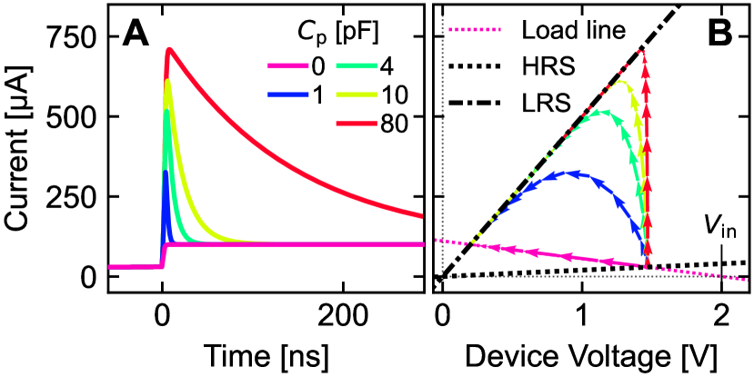
also known as the load line. For fast conductance switching events that are common in the targeted material systems, transient deviations from the load line occur as seen in the simplified situation of Fig. 2. During such transients, the excess energy delivered to the DUT due to capacitive discharge is significant and can strongly influence the end result of the switching process.
While the potential for overshooting transients is unavoidable in the context of a passive feedback arrangement, it is important that they are controlled to the extent possible and accurately measured when they occur. The only way that overshoots can be reduced in the discussed configuration is by minimizing the value of . Practically this means that a coaxial cable, acting approximately as a parasitic capacitance of 100 pF/m, cannot be used to connect to the DUT. The series resistance should rather be placed as close as possible to the DUT, with the components carefully selected and the printed circuit board (PCB) layout designed for low contribution to the total .
High fidelity current measurements can be achieved by amplification of the voltage across a ground referenced shunt termination following transmission over a coaxial line. Using this type of current measurement, positioning the DUT (rather than ) adjacent to the shunt is generally preferred because it avoids low pass filtering of the signal, allowing measurement of at a high bandwidth that is independent of the resistance state of the device. With prior knowledge of , Eq. 2 is often used to calculate the from a measurement of and , but there are several drawbacks associated with this method. One is the inaccuracy that comes from neglecting the capacitive currents of the left-hand side of Eq. 1. Another problem is measurement noise introduced by the term, as the small signal with high relative error is multiplied by a potentially large value. It is therefore advantageous to directly amplify the voltage at the DUT electrode rather than attempt to calculate it from other measured signals.
Following from these considerations, the basic intended configuration of external instruments and the designed circuit can be seen in Fig 3. If sufficient resolution is not obtained by sampling the current with a bare oscilloscope input, additional voltage amplification should be placed at the termination, where the use of several output stages is beneficial for dynamic range. Note that the length of the coaxial lines for DUT voltage and current sampling should be matched so that post-processing is not needed for signal synchronization.

A commercial integrated circuit, the DS1808 digipot from Maxim Integrated, was chosen as the central component to control the series resistance, . Internally it contains two separate potentiometers, each consisting of a chain of 32 resistors whose junctions can be connected to a "wiper" output via a set of CMOS transmission gates (analog switches). For each potentiometer, there are 32 available resistance settings spaced logarithmically (piecewise) from approximately to . According to the published specifications, the DS1808 has a maximum parasitic capacitance of 10 pF and a maximum voltage range of V[17].
To increase the coverage of values, the PCB is routed in a way that allows connection of both potentiometers either in series or in parallel by connecting or opening solder jumper pads. While a connection to a single potentiometer remains a possibility, the number of unique settings is increased to 528 between for the series combination and between for the parallel combination. Because a low resistance setting below 300 is not provided by the digipots, a reed switch was also included on the PCB to add an option to short the input directly to the output.
For amplification of the output voltage, a THS3091 current-feedback operational amplifier from Texas Instruments was used in a non-inverting configuration. This device features low distortion, low noise, a bandwidth of 210 MHz, and a slew rate of while adding only 0.1 pF parasitic capacitance[18].
All on-board settings are controlled via an Atmega32u4 microcontroller programmed as a USB serial interface to the PC. Control of the value is accessible using any programming language able to open a serial COM connection and send a simple command composed of three integer values corresponding to the wiper positions and the state of the bypass relay. The total time from issuing a serial command to reaching a new value is limited by USB / I2C communication, and is typically less than 300 s. The overall circuit design is visualized in the a block diagram of Fig 4, and a corresponding fabricated PCB is pictured in Fig. 5.


III Measurements
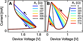
For quasistatic measurements of classical NDR materials using a series resistance, saddle-node bifurcations can occur that separate the NDR characteristic into stable and unstable regions. The range of the unstable region is determined by the value of the series resistor, with the bifurcations occurring where the derivative of the NDR curve voltage with respect to current crosses . While sweeping voltage, sudden current jumps are observed for sufficiently low values of in S-type NDR (Fig. 6A) and for sufficiently high values of in N-type NDR (Fig. 6B). Thus, an adaptable value allows control of the conditions under which each of these characteristic curves, which contain important information, can be measured.
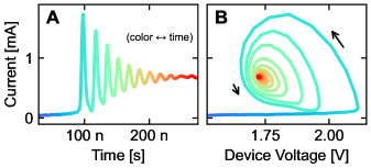
Where the material mechanism of NDR is dynamic and reversible, the presence of makes the measurement circuit prone to transient oscillations, and stable oscillatory limit cycles can also occur. Useful in these cases, the presented circuit is able to capture high speed transients and accurately project them onto the device plane (Fig. 7). This data can be used for device modelling and circuit simulations, each relevant for example in the ongoing investigations of coupled oscillatory devices in neuromorphic systems.
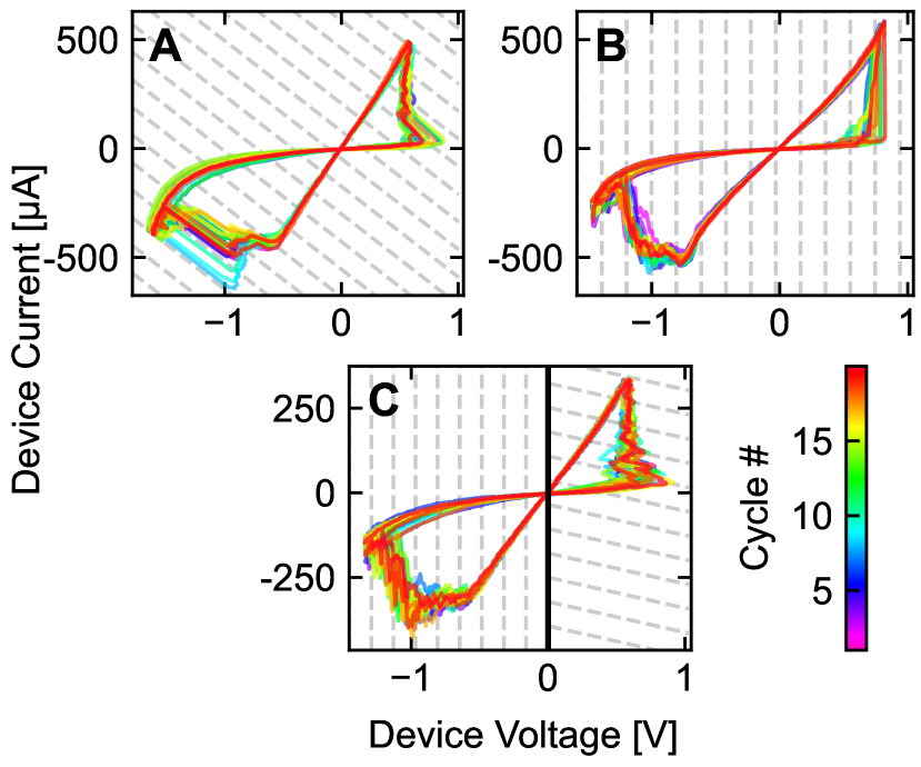
In ReRAM devices, NDR behavior is mediated by a combination of Joule heating and migration of point defects in the oxide material that locally increase its conductivity[4]. Altering the value allows these transitions to be probed in different ways, as seen in the example measurements of Fig. 8. In analogy to the NDR measurements of Fig. 6, a fixed value of can result in sudden and unstable transitions for one or both of the SET or RESET processes. By switching the value of during the measurement (Fig. 8C) it is observed that runaway load line transitions can be suppressed by appropriate selection of the external feedback.
IV Conclusion
When performing electrical measurements of resistive switching systems, the use of well understood circuitry is critical for realistic evaluation. With isolated devices vulnerable to runaway transitions, a series resistance circuit provides a simple means for control and tractable analysis of switching processes. In this context, parasitic capacitance is an important factor, and the values of both and lead to different switching outcomes in general. We have presented a circuit design for synchronized measurement of switching trajectories at high speed while using a programmable linear series resistance with low parasitic capacitance. Using this circuit, possible implications of the physical processes that accompany runaway transitions can be conveniently investigated, yielding insights into how optimal control can eventually be achieved.
Data Availability
The data that support the findings of this study are available from the corresponding author upon reasonable request.
References
- Burr et al. [2017] G. W. Burr, R. M. Shelby, A. Sebastian, S. Kim, S. Kim, S. Sidler, K. Virwani, M. Ishii, P. Narayanan, A. Fumarola, L. L. Sanches, I. Boybat, M. Le Gallo, K. Moon, J. Woo, H. Hwang, and Y. Leblebici, “Neuromorphic computing using non-volatile memory,” Adv. Phys. X 2, 89–124 (2017).
- Li et al. [2017] H. Li, T. F. Wu, S. Mitra, and H.-S. P. Wong, “Resistive RAM-Centric Computing: Design and Modeling Methodology,” IEEE Trans. Circuits Syst. I 64, 2263–2273 (2017).
- Sangwan and Hersam [2020] V. K. Sangwan and M. C. Hersam, “Neuromorphic nanoelectronic materials,” Nat. Nanotechnol. 15, 517–528 (2020).
- Waser et al. [2009] R. Waser, R. Dittmann, G. Staikov, and K. Szot, “Redox-Based Resistive Switching Memories - Nanoionic Mechanisms, Prospects, and Challenges,” Adv. Mater. 21, 2632–2663 (2009).
- Hardtdegen et al. [2016] A. Hardtdegen, C. La Torre, H. Zhang, C. Funck, S. Menzel, R. Waser, and S. Hoffmann-Eifert, “Internal Cell Resistance as the Origin of Abrupt Reset Behavior in HfO2-Based Devices Determined from Current Compliance Series,” in 2016 IEEE 8th International Memory Workshop (IMW) (IEEE, Paris, France, 2016) pp. 1–4.
- Ibáñez et al. [2021] M. J. Ibáñez, D. Barrera, D. Maldonado, R. Yáñez, and J. B. Roldán, “Non-Uniform Spline Quasi-Interpolation to Extract the Series Resistance in Resistive Switching Memristors for Compact Modeling Purposes,” Mathematics 9, 2159 (2021).
- Fantini et al. [2012] A. Fantini, D. J. Wouters, R. Degraeve, L. Goux, L. Pantisano, G. Kar, Y.-Y. Chen, B. Govoreanu, J. A. Kittl, and L. Altimime, “Intrinsic switching behavior in HfO2 RRAM by fast electrical measurements on novel 2R test structures,” in Memory Workshop (IMW), 2012 4th IEEE International (IEEE, 2012) pp. 1–4.
- Hennen et al. [2019] T. Hennen, D. Bedau, J. A. J. Rupp, C. Funck, S. Menzel, M. Grobis, R. Waser, and D. J. Wouters, “Switching Speed Analysis and Controlled Oscillatory Behavior of a Cr-Doped V2O3 Threshold Switching Device for Memory Selector and Neuromorphic Computing Application,” in 2019 IEEE 11th International Memory Workshop (IMW) (IEEE, Monterey, CA, USA, 2019) pp. 1–4.
- Gonzalez et al. [2020] M. B. Gonzalez, M. Maestro-Izquierdo, F. Jiménez-Molinos, J. B. Roldán, and F. Campabadal, “Current transient response and role of the internal resistance in HfOx-based memristors,” Appl. Phys. Lett. , 6 (2020).
- Maldonado et al. [2021] D. Maldonado, F. Aguirre, G. González-Cordero, A. M. Roldán, M. B. González, F. Jiménez-Molinos, F. Campabadal, E. Miranda, and J. B. Roldán, “Experimental study of the series resistance effect and its impact on the compact modeling of the conduction characteristics of HfO2-based resistive switching memories,” Journal of Applied Physics 130, 054503 (2021).
- Hardtdegen et al. [2018] A. Hardtdegen, C. La Torre, F. Cuppers, S. Menzel, R. Waser, and S. Hoffmann-Eifert, “Improved Switching Stability and the Effect of an Internal Series Resistor in HfO2/TiOx Bilayer ReRAM Cells,” IEEE Trans. Electron Devices 65, 3229–3236 (2018).
- Strachan et al. [2013] J. P. Strachan, A. C. Torrezan, F. Miao, M. D. Pickett, J. J. Yang, W. Yi, G. Medeiros-Ribeiro, and R. S. Williams, “State Dynamics and Modeling of Tantalum Oxide Memristors,” IEEE Trans. Electron Devices 60, 2194–2202 (2013).
- Kinoshita et al. [2008] K. Kinoshita, K. Tsunoda, Y. Sato, H. Noshiro, S. Yagaki, M. Aoki, and Y. Sugiyama, “Reduction in the reset current in a resistive random access memory consisting of NiOx brought about by reducing a parasitic capacitance,” Appl. Phys. Lett. 93, 033506 (2008).
- Lu et al. [2012] Y. M. Lu, M. Noman, W. Chen, P. A. Salvador, J. A. Bain, and M. Skowronski, “Elimination of high transient currents and electrode damage during electroformation of TiO 2-based resistive switching devices,” J. Phys. Appl. Phys. 45, 395101 (2012).
- Sharma et al. [2014] A. A. Sharma, M. Noman, M. Abdelmoula, M. Skowronski, and J. A. Bain, “Electronic Instabilities Leading to Electroformation of Binary Metal Oxide-based Resistive Switches,” Adv. Funct. Mater. 24, 5522–5529 (2014).
- Meng et al. [2020] J. Meng, B. Zhao, Q. Xu, J. M. Goodwill, J. A. Bain, and M. Skowronski, “Temperature overshoot as the cause of physical changes in resistive switching devices during electro-formation,” J. Appl. Phys. 127, 235107 (2020).
- DS1 [2001] DS1808 Dual Log Digital Potentiometer, Maxim Integrated (2001), archived at https://perma.cc/VK7V-8MSG.
- THS [2015] THS309x High-voltage, Low-distortion, Current-feedback Operational Amplifiers, Texas Instruments (2015), archived at https://perma.cc/PQX3-RUZD.
- Hennen et al. [2018] T. Hennen, D. Bedau, J. A. J. Rupp, C. Funck, S. Menzel, M. Grobis, R. Waser, and D. J. Wouters, “Forming-Free Mott-Oxide Threshold Selector Nanodevice Showing s-Type NDR with High Endurance ( 1012 Cycles), Excellent Vth Stability ( 5%), Fast ( 10 ns) Switching, and Promising Scaling Properties,” in IEDM (San Francisco, CA, USA, 2018) pp. 37.5.1–37.5.4.
- Hennen et al. [2021] T. Hennen, E. Wichmann, A. Elias, J. Lille, O. Mosendz, R. Waser, D. J. Wouters, and D. Bedau, “Current-limiting amplifier for high speed measurement of resistive switching data,” Rev Sci Instrum , 7 (2021).