Spin polarisation and non-isotropic effective mass in the conduction band of GdN
Abstract
GdN is a ferromagnetic semiconductor which has seen increasing interest in the preceding decades particularly in the areas of spin- and superconducting- based electronics. Here we report a detailed computational study and optical spectroscopy study of the electronic structure of stoichiometric and nitrogen vacancy doped GdN. Based on our calculations we provide the effective mass tensor for undoped GdN, and some indicative values for electron doped GdN. Such a property is valuable as it can directly affect device design, and be directly measured experimentally to validate the existing computation results.
pacs:
71.27.+a, 75.50.PpI Introduction
The increasing global demand for computational efficiency Andrae (2015) has pushed the development of conventional CMOS based logic and memory beyond the imagination of the materials scientists and physicists who pioneered the first generation of transistor based devices decades ago. With the limits of the present family of conventional-materials based devices (perpetually) on the horizon there has been an ongoing effort to design more exotic logic and memory systems, systems which can surpass the conventional technologies leading to orders of magnitude increases in operating efficiency and speed IRD (2018a, b).
Among the most attractive of these technologies are spintronics Hirohata et al. (2020); Bhatti et al. (2017) and superconducting electronics Soloviev et al. (2017); Likharev and Semenov (1991). Both of these operate at cryogenic temperatures, temperatures which limit the use of conventional materials. As such, a search for materials with the functionalities required for these technologies and the ability to operate at the required temperatures is an active area of materials science Li and Yang (2016); Shamiul Alam (2023). In this context the rare-earth nitride (LN - L a lanthanide) series of ferromagnetic semiconductors Natali et al. (2010) has seen a burst of interest in recent years. First studied in the 1950s Eick et al. (1956) the LN were found to be mostly ferromagnetic with Curie temperatures on the order of 50 K Hulliger (1978). The simple rock-salt structure and limited quenching of the orbital angular momentum results in rich and varied magnetic behaviours across the series, which is driven by the 4f occupation ranging from 0 in LaN to 14 in LuN. The series was initially thought to be half-metallic, similar to the other rare-earth pnicitdes Hulliger (1979). However, improved experimental procedures allowing the growth of high quality thin films, along with improved computational methods, has in recent decades revealed the semiconducting nature of at least several members of the series Granville et al. (2006); Aerts et al. (2004); Anton et al. (2016); Holmes-Hewett et al. (2020, 2023); Devese et al. (2022).
GdN is the most studied of the rare-earth nitrites, with a Curie temperature reported between 50 K and 70 K Ludbrook et al. (2009). The half filled 4f shell yields a strong magnetic moment of 7 per Gd ion, or 32 per nm3. GdN is insulating in the stoichiometric state with a valence band formed from N 2p states and a conduction band minimum formed from Gd 5d states. The stoichiometric band structure calculated in the present study is shown in Figure 1. The valence band maximum is at and there is a 0.9 eV optical band gap between the majority spin states at the X point Trodahl et al. (2007), to which we have tuned our calculation (see section II). The minority spin gap is significantly larger in the calculation ( 2.5 eV) between the minority spin N 2p and Gd 5d states at X, a result of a large spin-splitting in the conduction ( eV) and the valence ( eV) bands both resulting from exchange with the Gd 4f states Larson and Lambrecht (2006). Previous computational studies Larson et al. (2007); Preston et al. (2010), also tuned to the optical gap in the ferromagnetic phase, find a significantly smaller minority spin gap of eV.
The onset of optical absorption in the ferromagnetic phase represents the majority spin gap, as both the conduction band minimum and valence band maximum are majority spin. There is largely agreement in the existing experimental studies regarding the 0.9 eV majority spin gap Trodahl et al. (2007); Vilela et al. (2024); Azeem (2016); Yoshitomi et al. (2011). There is however much less agreement regarding the minority spin gap and associated spin-splitting, the latter of which is reported variously as 0.16 eV, 0.4 eV and 0.6 eV respectively in Refs Vidyasagar et al. (2012); Azeem (2016) and Vilela et al. (2024). In the context of majority-minority spin gaps the paramagnetic gap can be estimated as an average of the two. The present calculation shown in Figure 1 yields 1.75 eV, somewhat above the experimental paramagnetic gap of 1.5 eV.
As with many of the other rare earth nitrides GdN can be doped with electrons though the inclusion of nitrogen vacancies Maity et al. (2018); Holmes-Hewett et al. (2020); Devese et al. (2022). These have a low activation energy, dependent on growth conditions Punya et al. (2011), so can be readily formed in thin films to the order of a few % by either reducing the N2 partial pressure during deposition, or controlling the substrate temperature. Experimental results on intentionally doped GdN films support the simple argument of the nitrogen vacancy donors raising the Fermi level into the (initially) majority spin only Gd 5d bands Trodahl et al. (2017).

The rare confluence of a combine semiconducting-ferromagnetic ground state has seen GdN included in many prototype cryogenic devices. The material is particularly attractive in the area of superconducting spintronics. The inclusion of ferromagnetic materials as the weak link in a Josephson junction structure adds functionality based on the hysteric nature of the magnetisation Birge and Satchell (2024), however the low resistance of the ferromagnetic-metals commonly used results in switching speeds orders of magnitude lower than in conventional superconducting logic, rendering conventional ferromagnetic-metal based Josephson junctions incompatible Vernik et al. (2013). In this context GdN has been used as the ferromagnetic insulator of choice in the superconducting spintronics community, with various devices already demonstrated including superconducting- spin-filters Senapati et al. (2011); Massarotti et al. (2015); Ahmad et al. (2020), diodes Sharma et al. (2023), primitive memory devices Cascales et al. (2019); Pot et al. (2023), and even the recent proposal of a GdN based ferro-transmon qubit Ahmad et al. (2022).
Given the roughly a decade of intense interest in the application of GdN in such devices it is surprising that the most recent computational studies regarding the electronic structure of GdN are themselves over a decade old Larson et al. (2007); Punya et al. (2011); Mitra and Lambrecht (2008). In the present manuscript we attempt to fill this void by undertaking a computational study of GdN, informed by experiment, where we aim to provide details regarding electron transport in GdN and realistic material parameters which will aid experimentalists and engineers in device design.
II Methods
II.1 Computational
Density functional theory (DFT) based calculations were undertaken using Quantum Espresso Giannozzi et al. (2009); Cococcioni and de Gironcoli (2005) and rare earth pseudo-potentials developed using the rare-earth nitrides Topsakal and Wentzcovitch (2014). Self-consistent calculations on the primitive cell were completed using a -mesh with divisions, while super-cell calculations were on a division k-mesh. The wave function and charge density cut-off energies were 50 Ry and 200 Ry respectively for all calculations. Following our DFT calculations the output from Quantum Espresso was used to generate maximally localised Wannier functions using Wannier 90 Mostofi et al. (2014); Marzari and Vanderbilt (1997); Souza et al. (2001). The resulting Wannier functions were then used to calculate the electronic properties on denser k meshes, a grid for calculation of the density of states and Fermi level) and a grid for the optical conductivity. The effective mass was determined using conventional DFT based on 400 k along each high symmetry direction.
The 4 electrons of the LnN series are strongly correlated and thus require careful treatment beyond the traditional DFT methods Larson and Lambrecht (2006); Larson et al. (2007). In the basic DFT the 4 states are found at or near the Fermi level for most of the stoichiometric rare earth nitrides, when in reality this is not the case. The strongly correlated nature of these electrons pushes the filled states below and unfilled states above the Fermi level. This physics can be approximated using the DFT+ method where the behaviour of the correlated orbitals is determined by an adjustable parameter . In the present study two parameters are used, as described first in reference Larson and Lambrecht (2006). One to account for the strongly correlated 4 states (), and a second applied to the 5 states () to adjust to the experimental optical band gap in the ferromagnetic phase. The process is discussed further in references Holmes-Hewett (2021) and Holmes-Hewett et al. (2023).
II.2 film growth and optical spectroscopy
GdN thin films on the order of 100 nm were prepared in a Thermionics ultrahigh vacuum chamber with a base pressure of mbar. Gd metal was evaporated by an electron gun in a N2 partial pressure of mbar at a rate of Å s-1. Varying the N2 growth pressure acts to control the concentration of nitrogen vacancies (VN) in the films. The films were capped with nm insulating AlN to minimise deterioration when exposed atmospheric water vapour and oxygen. The films were simultaneously deposited at ambient temperature on Si and Al2O3 substrates to suit the required measurements.
Samples for electrical transport measurements were deposited on mm2 Al2O3 substrates predeposited with Cr/Au contacts in the van der Pauw configuration. Electrical measurements were conducted in a Janis closed-cycle helium cryostat and a Quantum Design Physical Properties System at temperatures from 300 to 4 K. Reflection and transmission measurements were performed with a Bruker Vertex 80v Fourier transform spectrometer in the 0.012-3 eV spectral range using films deposited on both Si and Al2O3 substrates. The reflectivity was measured relative to a 200 nm Al film and then corrected for the finite reflectivity of Al using data from Ehrenreich Ehrenreich et al. (1963). The reflectivity and transmission spectra were simultaneously modelled with refFIT software Kuzmenko (2005) using a Kramers-Kronig consistent consistent sum of Drude-Lorentzians to calculate the energy-dependent dielectric function from which the presented optical conductivity data was generated.
III Results
III.1 Density function theory
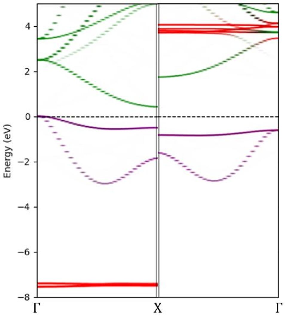
As is commonly reported, GdN is grown with varying nitrogen vacancy doping to control the carrier concentration. In the doped crystal the Gd ions in the lattice retain their 3+ oxidation state, so to maintain charge neutrality the three electrons formerly on the nitrogen ion must be accounted for. Two electrons occupy defect states which localise to the vacancy site, while the third electron finds a higher energy defect state, drawing the Fermi level up into the extended state Gd 5d conduction band. This one mobile electron per nitrogen vacancy is responsible for electron transport. The Fermi surface is then a prolate spheroid with its centre at the X point, major axis pointing along X and minor axes in the XW and XU plane. The first Brillouin zone with the Fermi surface highlighted is shown in the inset to Figure 2. It is then the dispersion along these three high symmetry directions which will dictate the transport properties of the material.
To represent the above description Figure 2 shows the calculated band structure of nitrogen vacancy doped GdN along these high symmetry directions. It is clear that the curvature of the bands contrasts significantly, resulting in a differing effective mass, and ultimately transport properties along different high symmetry directions. The figure shows the calculated wave-functions projected onto the atomic orbitals (colours noted in caption), in addition we have calculated the dispersion for the stoichiometric Gd 5d conduction band along the same high symmetry directions, shown for the majority spin as black dashed lines in the left hand panel of Figure 2. It is significant that the stoichiometric and nitrogen vacancy doped conduction bands are essentially superimposed on one another, fitting the picture that the electrons donated by nitrogen vacancy doping are simply lifting the Fermi level into the intrinsic conduction band. Although the shape of the bands is retained between the stoichiometric and doped calculations the gap between the Gd 5d and N 2p states at the X point has reduced from 0.9 eV in the stoichiometric case to 0.6 eV in the doped case, the renormalzation likely a result of screening from the delocalised electrons. The onset of optical absorption is still near 0.9 eV, however now between and X, and expected to be much weaker as the initial states are the occupied defect states, here with a concentration of only 1/27 to that of the N 2p. The intrinsic majority spin optical band gap (i.e. not involving defect states) increases to 1.2 eV ( 0.9 eV in the stoichiometric crystal) in a Moss-Berstein like shift.
The minority spin states are shown in the right hand panel of Figure 2. The Gd 5d states are again very similar to the stoichiometric crystal. However, the presence of the occupied defect states in the gap, below the Fermi level, effectively reduces minority spin optical gap from 2.5 eV in the stoichiometric to 1.8 eV in the doped crystal. The average absorption onset of the majority and minority spin gaps in the doped crystal (both with initial impurity states and Gd 5d final states) is now 1.35 eV (1.75 eV in the stoichiometric crystal). This is now less than is commonly reported for the paramagnetic band gap.
Using the present results from the doped crystal the spin splitting can be reported in various ways. The most appropriate for electrical transport (i.e. as in a spin filter) is the minimum energy difference between available (hole or electron) majority and minority spin states. As Fermi level lies in the majority spin Gd 5d band, for electron carriers this is the energy difference between the Fermi level and the bottom of the minority spin conduction band, roughly 1.1 eV, while for hole carriers this is the energy difference between the Fermi level and the top of the minority spin valance band, roughly 0.6 eV. For optical studies the most relevant spin splitting is the difference between the majority spin and minority spin optical gaps, which now 0.9 eV. This is closer to the experimental reports, yet still beyond the maximum 0.6 eV reported in reference Vilela et al. (2024).
III.2 Optical spectroscopy

As an initial comparison of our computational results to experiment we have calculated the optical conductivity for both the pristine and doped cells discussed above. These are displayed in Figure 3. The top panel of Figure 3 shows the calculated optical conductivity for stoichiometric GdN. The onset of optical absorption is in the majority spin states at 0.9 eV and initially shows an increase with a near form, which is expected from the Van Hove singularity at the conduction band minimum. Above 2 eV the gradient increases relating to the flattening of both the 5d and the N 2p bands near +2 eV and -2 eV respectively. At roughly 2.5 eV there is a similar onset of absorption in the minority spin states. The inset show the spectra between 0.8 eV and 3 eV now with experimental data (blue) measured at 8 K. Although the onset of absorption is a roughly the same energy in both spectra the form is very different, with the experiment not taking the typical shape expected for the onset of optical transitions in a parabolic band.
The lower panel of Figure 3 shows the calculated optical conductivity for the nitrogen vacancy doped super-cell. Here, as discussed in section III.1, the absorption onset is at roughly the same energy (0.9 eV) as the pristine cell. For the doped material the form of the optical conductivity differs greatly from the simple shape as the Fermi level now lies within the conduction band. The inset again shows the comparison between the calculation and experiment with a clear qualitative similarity between the two (the calculation has been scaled by a factor of 0.2 to best match the experiment). The film used for the measurement was moderately conductive with a resistivity of 0.1 cm at room temperature, increasing to 10 cm at 4 K. Given this resistivity, and based on Hall measurements on other films Lee et al. (2015), one could assume a carrier concentration on the order 10 17cm-3 at 4 K, however the striking resemblance between the optical spectra for this film and the super-cell calculation (carrier concentration cm-3) may rather imply that in this is incorrect. This film and possibly other nominally undoped rare-earth nitrides may harbour a significant population of localised carriers. These do not contribute to electron transport in the usual extended state manner; however, they do occupy states at the bottom of the conduction band, affecting the optical spectra and other related electrical properties. Similar optical spectra have been seen in other rare-earth nitrides Holmes-Hewett et al. (2019, 2020, 2023) and along with electrical transport measurements were discussed in the context of localised hopping type conductivity and a mobility edge scenario.
III.3 Effective mass
Although the details of the spin-splitting and related exchange energy remain to be determined the present data, calculations and existing experimental reports Trodahl et al. (2017) seem to agree that when GdN is doped with electrons via nitrogen vacancies the Fermi level is raised into the Gd 5d band, which is majority spin only at dilute to moderate doping levels. Motivated by these observations, and the similarity between the stoichiometric and nitrogen vacancy doped Gd 5d bands we have used the former to calculate the effective mass along the X, XW and XU directions, which may be of use in the context of device design. The results are shown in Figure 4 with the dispersion along the X, XW and XU directions in the top panel, and the effective mass in the bottom panel, both as a function of wave-vector measured relative to the X point at .
At the X point the first Brillouin zone of the FCC lattice has four-fold symmetry (see inset of Figure 2), which dictates that along any two directions in the plane of the X-face the effective mass is degenerate at X. Without loss of generality we choose directions along XU and XW to form our basis, the final perpendicular direction is then along X and will have a distinct effective mass at the X point. The X effective mass tensor is diagonal in this coordinate system and given by
The enhanced curvature along the XU and XW directions results in an order of magnitude effective mass difference between the longitudinal and transverse directions of the Fermi surface. Using these values we can estimate the conductivity effective mass as , which is dominated by the low mass components. Given the relative orientation between the equivalent X points in the first Brillouin zone an electrical field along any direction will result in contributions from both the transverse the longitudinal directions. The order of magnitude lower mass in the transverse direction will result in this dominating in any electrical transport measurement.
The effective mass precisely at the X point is useful in the context of tunnelling experiments where the GdN is likely intended to be insulating and close to stoichiometric, in addition the geometry of these experiments is well controlled and for example the common case of NbN/GdN/NbN multi-layers Senapati et al. (2011) results in transport through the GdN along a 001 direction. As discussed above the degeneracy of the X point results in contributions from both the transverse and longitudinal directions; at the X point the combination of these contributions can in principle be easily treated.
As one dopes the crystal with electrons the Fermi surface expands from the X point and the effective mass is a function of wavevector as shown in Figure 4. Along the X direction the effective mass is relatively stable with a slight drop before an increase near . As one continues along this direction there is ultimately a sign inversion near the first Brillouin zone boundary as the curvature of the band itself changes sign.
Due to the rapidly changing mass along the two transverse directions it may be difficult to predict the transport properties of even moderately electron doped GdN. The super-cell used in the calculation of Figure 2 was constructed from primitive unit cells with a N atom removed. The single mobile electron in a volume of results in a carrier concentration of 1cm-3 and is representative of the heavily doped GdN from experimental reports Maity et al. (2018). The presence of this electron raises the Fermi level roughly 0.6 eV into the conduction band, the resulting Fermi wave vectors are indicated on Figure 4. Far from the X point the effective mass tensor will no longer take the simple diagonal form presented above, but even so the wave vector dependent effective mass shown in Figure 4 gives a qualitative indication of the evolution of the effective mass with electron doping in GdN.

IV Conclusions
We have undertaken a computational study of the band structure and defect states in stoichiometric and nitrogen vacancy doped GdN. Our most direct result is the effective mass tensor at the X point, and calculation of the effective mass in the high symmetry directions moving away from the centre of this pocket. We have provided updated band structure calculations of GdN and compared these to conventional optical spectroscopy. The comparison between conventional spectroscopy and the calculation indicates that even nominally dilutly doped GdN has evidence of a large population of localised carriers in occupying states at the conduction band minimum.
V Data Availability
The data used during this study are available from the corresponding author upon reasonable request.
VI ACKNOWLEDGMENTS
This research was supported by Quantum Technologies Aotearoa, a research programme of Te Whai Ao – the Dodd Walls Centre, funded by the New Zealand Ministry of Business Innovation and Employment through International Science Partnerships, contract number UOO2347. The computations were performed on the Rāpoi high performance computing facility of Victoria University of Wellington.
References
- Andrae (2015) T. Andrae, A.S.G.; Edler, Challenges 6, 117 (2015).
- IRD (2018a) International roadmap for devices and systems - Beyond CMOS (2018).
- IRD (2018b) International roadmap for devices and systems - More Moore (2018).
- Hirohata et al. (2020) A. Hirohata, K. Yamada, Y. Nakatani, I.-L. Prejbeanu, B. Diény, P. Pirro, and B. Hillebrands, Journal of Magnetism and Magnetic Materials 509, 166711 (2020).
- Bhatti et al. (2017) S. Bhatti, R. Sbiaa, A. Hirohata, H. Ohno, S. Fukami, and S. Piramanayagam, Materials Today 20, 530 (2017).
- Soloviev et al. (2017) I. I. Soloviev, N. V. Klenov, S. V. Bakurskiy, M. Y. Kupriyanov, A. L. Gudkov, and A. S. Sidorenko, Beilstein Journal of Nanotechnology 8, 2689 (2017).
- Likharev and Semenov (1991) K. Likharev and V. Semenov, IEEE Transactions on Applied Superconductivity 1, 3 (1991).
- Li and Yang (2016) X. Li and J. Yang, National Science Review 3, 365 (2016).
- Shamiul Alam (2023) S. R. S. . A. A. Shamiul Alam, Md Shafayat Hossain, Nature Electronics 6, 185–198 (2023).
- Natali et al. (2010) F. Natali, N. O. Plank, J. Galipaud, B. J. Ruck, H. J. Trodahl, F. Semond, S. Sorieul, and L. Hirsch, Journal of Crystal Growth 312, 3583 (2010).
- Eick et al. (1956) H. A. Eick, N. C. Baenziger, and L. Eyring, Journal of the American Chemical Society 78, 5987 (1956).
- Hulliger (1978) F. Hulliger, Journal of Magnetism and Magnetic Materials 8, 183 (1978).
- Hulliger (1979) F. Hulliger, in Non-Metallic Compounds - II, Handbook on the Physics and Chemistry of Rare Earths, Vol. 4 (Elsevier, 1979) pp. 153 – 236.
- Granville et al. (2006) S. Granville, B. J. Ruck, F. Budde, A. Koo, D. J. Pringle, F. Kuchler, A. R. H. Preston, D. H. Housden, N. Lund, A. Bittar, G. V. M. Williams, and H. J. Trodahl, Phys. Rev. B 73, 235335 (2006).
- Aerts et al. (2004) C. M. Aerts, P. Strange, M. Horne, W. M. Temmerman, Z. Szotek, and A. Svane, Phys. Rev. B 69, 045115 (2004).
- Anton et al. (2016) E.-M. Anton, J. F. McNulty, B. J. Ruck, M. Suzuki, M. Mizumaki, V. N. Antonov, J. W. Quilty, N. Strickland, and H. J. Trodahl, Phys. Rev. B 93, 064431 (2016).
- Holmes-Hewett et al. (2020) W. F. Holmes-Hewett, C. Pot, R. G. Buckley, A. Koo, B. J. Ruck, F. Natali, A. Shaib, J. D. Miller, and H. J. Trodahl, Appl. Phys. Lett. 117, 222409 (2020).
- Holmes-Hewett et al. (2023) W. F. Holmes-Hewett, K. V. Koughnet, J. D. Miller, E. X. M. Trewick, B. J. Ruck, H. J. Trodahl, and R. G. Buckley, Sci Rep 13 (2023).
- Devese et al. (2022) S. Devese, K. Van Koughnet, R. G. Buckley, F. Natali, P. P. Murmu, E.-M. Anton, B. J. Ruck, and W. F. Holmes-Hewett, AIP Advances 12, 035108 (2022).
- Ludbrook et al. (2009) B. Ludbrook, I. Farrell, M. Kübel, B. Ruck, A. Preston, J. Trodahl, L. Ranno, R. Reeves, and S. Durbin, Journal of Applied Physics 106, 063910 (2009).
- Trodahl et al. (2007) H. J. Trodahl, A. R. H. Preston, J. Zhong, B. J. Ruck, N. M. Strickland, C. Mitra, and W. R. L. Lambrecht, Phys. Rev. B 76, 085211 (2007).
- Larson and Lambrecht (2006) P. Larson and W. R. L. Lambrecht, Phys. Rev. B 74, 085108 (2006).
- Larson et al. (2007) P. Larson, W. R. L. Lambrecht, A. Chantis, and M. vanSchilfgaarde, Phys. Rev. B 75, 045114 (2007).
- Preston et al. (2010) A. R. H. Preston, B. J. Ruck, W. R. L. Lambrecht, L. F. J. Piper, J. E. Downes, K. E. Smith, and H. J. Trodahl, Appl. Phys. Lett. 96, 032101 (2010).
- Vilela et al. (2024) G. L. S. Vilela, G. M. Stephen, X. Gratens, G. D. Galgano, Y. Hou, Y. Takamura, D. Heiman, A. B. Henriques, G. Berera, and J. S. Moodera, Phys. Rev. B 109, L060401 (2024).
- Azeem (2016) M. Azeem, Chin. Phys. Lett. 33, 027501 (2016).
- Yoshitomi et al. (2011) H. Yoshitomi, S. Kitayama, T. Kita, O. Wada, M. Fujisawa, H. Ohta, and T. Sakurai, Phys. Rev. B 83, 155202 (2011).
- Vidyasagar et al. (2012) R. Vidyasagar, S. Kitayama, H. Yoshitomi, T. Kita, T. Sakurai, and H. Ohta, Appl. Phys. Lett. 100, 232410 (2012).
- Maity et al. (2018) T. Maity, H. J. Trodahl, F. Natali, B. J. Ruck, and S. Vézian, Phys. Rev. Materials 2, 014405 (2018).
- Punya et al. (2011) A. Punya, T. Cheiwchanchamnangij, A. Thiess, and W. Lambrecht, MRS Proceedings 1290 (2011).
- Trodahl et al. (2017) H. J. Trodahl, F. Natali, B. J. Ruck, and W. R. L. Lambrecht, Phys. Rev. B 96, 115309 (2017).
- Birge and Satchell (2024) N. O. Birge and N. Satchell, APL Materials 12, 041105 (2024).
- Vernik et al. (2013) I. V. Vernik, V. V. Bol’ginov, S. V. Bakurskiy, A. A. Golubov, M. Y. Kupriyanov, V. V. Ryazanov, and O. A. Mukhanov, IEEE Transactions on Applied Superconductivity 23, 1701208 (2013).
- Senapati et al. (2011) K. Senapati, M. G. Blamire, and Z. H. Barber, Nat. Mater. 10, 849 (2011).
- Massarotti et al. (2015) D. Massarotti, A.Pal, G. Rotoli, L. Longobardi, M. Blamire, and F. Tafuri, Nature Communications 6, 7376 (2015).
- Ahmad et al. (2020) H. Ahmad, R. Caruso, A. Pal, G. Rotoli, G. Pepe, M. Blamire, F. Tafuri, and D. Massarotti, Phys. Rev. Appl. 13, 014017 (2020).
- Sharma et al. (2023) P. K. Sharma, S. Banerjee, B. Dutta, V. Singhal, P. Banerjee, H. K. Pal, and A. Pal, (2023), arXiv:2312.04650 [cond-mat.supr-con] .
- Cascales et al. (2019) J. P. Cascales, Y. Takamura, G. M. Stephen, D. Heiman, F. S. Bergeret, and J. S. Moodera, Applied Physics Letters 114, 022601 (2019).
- Pot et al. (2023) C. Pot, W. F. Holmes-Hewett, E.-M. Anton, J. D. Miller, B. J. Ruck, and H. J. Trodahl, Appl. Phys. Lett. 13 (2023).
- Ahmad et al. (2022) H. G. Ahmad, V. Brosco, A. Miano, L. Di Palma, M. Arzeo, D. Montemurro, P. Lucignano, G. P. Pepe, F. Tafuri, R. Fazio, and D. Massarotti, Phys. Rev. B 105, 214522 (2022).
- Mitra and Lambrecht (2008) C. Mitra and W. R. L. Lambrecht, Phys. Rev. B 78, 195203 (2008).
- Giannozzi et al. (2009) P. Giannozzi et al., J. Phys.: Condens. Matter 21, 395502 (2009).
- Cococcioni and de Gironcoli (2005) M. Cococcioni and S. de Gironcoli, Phys. Rev. B 71, 035105 (2005).
- Topsakal and Wentzcovitch (2014) M. Topsakal and R. Wentzcovitch, Comput. Mater. Sci. 95, 263 (2014).
- Mostofi et al. (2014) A. A. Mostofi, J. R. Yates, G. Pizzi, Y.-S. Lee, I. Souza, D. Vanderbilt, and N. Marzari, Computer Physics Communications 185, 2309 (2014).
- Marzari and Vanderbilt (1997) N. Marzari and D. Vanderbilt, Phys. Rev. B 56, 12847 (1997).
- Souza et al. (2001) I. Souza, N. Marzari, and D. Vanderbilt, Phys. Rev. B 65, 035109 (2001).
- Holmes-Hewett (2021) W. F. Holmes-Hewett, Phys. Rev. B 104, 075124 (2021).
- Ehrenreich et al. (1963) H. Ehrenreich, H. R. Philipp, and B. Segall, Phys. Rev. 132, 1918 (1963).
- Kuzmenko (2005) A. B. Kuzmenko, Rev. Sci. Instrum. 76, 083108 (2005).
- Lee et al. (2015) C. M. Lee, H. Warring, S. Vézian, B. Damilano, S. Granville, M. Al Khalfioui, Y. Cordier, H. J. Trodahl, B. J. Ruck, and F. Natali, Appl. Phys. Lett. 106, 022401 (2015).
- Holmes-Hewett et al. (2019) W. F. Holmes-Hewett, R. G. Buckley, B. J. Ruck, F. Natali, and H. J. Trodahl, Phys. Rev. B 99, 205131 (2019).