Spectral broadening of optical transitions at tunneling resonances in InAs/GaAs coupled quantum dot pairs
Abstract
We report on linewidth analysis of optical transitions in InAs/GaAs coupled quantum dots as a function of bias voltage, temperature, and tunnel coupling strength. A significant line broadening up to 100 eV is observed at hole tunneling resonances where the coherent tunnel coupling between spatially direct and indirect exciton states is maximized, corresponding to a phonon-assisted transition rate of at 20 K. With increasing temperature, the linewidth shows broadening characteristic of single-phonon transitions. The linewidth as a function of tunnel coupling strength tracks the theoretical prediction of linewidth broadening due to phonon-assisted transitions, and is maximized with an energy splitting between the two exciton branches of meV. This report highlights the linewidth broadening mechanisms and fundamental aspects of the interaction between these systems and the local environment.
I Introduction
Vertically stacked coupled quantum dot (CQD) pairs embedded in an electric field effect structure allow for wide-range tuning of atom-like charge and spin states due to an enhanced quantum confined Stark effect (QCSE).Ramanathan et al. (2013); Scheibner et al. (2009); Stinaff et al. (2006) Optically generated electron-hole pairs can be localized in one of the dots, the electron and hole can be localized in separate dots, or they can be delocalized in both quantum dots by forming a molecular exciton state. The coupling between two dots is quantified by the tunnel coupling strength. The coherent manipulation of exciton states and control of interdot coupling in CQDs offers advantages for CQD-based quantum devices for optical sensing and quantum information processing.Jennings et al. (2019); Kim et al. (2011); Loss and DiVincenzo (1998); Scheibner et al. (2012); Gao et al. (2012); Vora et al. (2015); Knill et al. (2001); Bayer et al. (2001) The pure dephasing, phonon relaxation and charges surrounding the quantum dots are a few major challenges hindering this venture.Borri et al. (2003); Muljarov et al. (2005); Bardot et al. (2005); Climente et al. (2006); Nakaoka et al. (2006); Gawarecki et al. (2010); Gawarecki and Machnikowski (2012); Wijesundara et al. (2011); Rolon et al. (2012); Müller et al. (2012, 2013); Daniels et al. (2013) These phenomena are coupled to the linewidth broadening and line profile, providing details of coupling to the local environment. The pure dephasing expresses the time scale of coherent interactions of charge states with lattice phonons. Other reports highlight charge fluctuation-induced broadening of indirect excitons in CQDs.Daniels et al. (2013); Ha et al. (2015); Zhou et al. (2013) The linewidth analysis of different charge states and dependence on applied field, including the tunneling resonances where one charge is delocalized, has fundamental research interest and is important to understand the quantum systems for potential quantum computing and sensing applications.
In this paper, we report the detailed analysis of linewidth broadening of direct and indirect excitons and examine the linewidth as a function of electric field near tunneling resonances. We investigate the hypothesis of broadening mechanisms as a function of temperature and tunnel coupling strength. These measurements explore the interaction of the optical transitions in quantum system with the local environment and adjacent charges.

II Experimental Methods and Results
Molecular beam epitaxy-grown, vertically stacked self-assembled InAs/GaAs quantum dot pairs with 4 nm interdot barrier thickness embedded in a Schottky diode structure are used in this study. The Schottky diode structure allows application of electric field to tune the energy band diagram by shifting the relative energy levels and favors the tunneling of charge carriers between the quantum dots. The details of the fabrication procedure are described elsewhere.Kerfoot et al. (2014) A variable wavelength CW diode laser operating at wavelength nm and power density is used to excite the CQDs quasi-resonantly. The laser beam is focused on the sample at an angle of 45 degrees to minimize the collection of scattered light. The emission from quantum dot molecules is collected with a 50X magnification microscope objective, dispersed by a triple spectrometer in additive configuration, then subsequently collected using a liquid nitrogen cooled CCD camera. The photoluminescence (PL) energy resolution is limited by the spectrometer response of eV for m slit opening. A 2600 series Keithley sourcemeter with 6.5-digit resolution is used to apply the electric field along the growth direction of the CQD pair. These measurements are done in a closed cycle helium cooled cryostat at temperatures of K, where K is the minimum attainable temperature of the cryostat.

The characteristic electric field dispersed optical transition energy map for one of the CQDs is shown in Figure 1a. This map is generated by fine stepping the applied voltage (in mV increments) along the growth direction of the self-assembled CQD and collecting the corresponding PL. The small separation of 4 nm between the quantum dots allows electron/hole tunneling when electronic levels are brought in resonance by applied electric field skewing the band structure in the intrinsic region of the Schottky-type diode. The PL bias map of the CQD shows multiple optical transitions appearing and disappearing as a function of bias. Every single optical transition is assigned to a charging state based on the spatial location of charge carrier generated. Scheibner et al. (2009, 2008) Here, we focus our analysis on the spectral broadening of the neutral exciton optical transitions, which generate the two most prominent lines in the electric field dispersed PL spectrum of Fig. 1a. The two transitions form an anticrossing (AC) in the center of the image. This anticrossing is a result of a hole level resonance between a direct exciton (), with an electron and hole in the bottom dot, and an indirect exciton (), with an electron in the bottom dot and hole in the top dot. The PL emission energy of the direct exciton shows a weak dependence on electric field, while that of the indirect exciton shows a strong electric field dependence. This difference in response to the electric field is a result of the static dipole moment , defined by the elementary charge and the spatial separation of electron and hole. The avoided crossing is the spectral signature of the formation of molecular states, i.e. the symmetric and anti-symmetric mixing of the direct and indirect excitons’ wavefunctions, .Doty et al. (2009) The resulting exciton state, , should exhibit properties in between that of the direct and the indirect exciton. For example, at the center of the anticrossing the Stark shift is the average of the Stark shift observed for the direct and indirect excitons. Likewise, the radiative lifetime at the center of the anticrossing can be expected to be the arithmetic average of the lifetimes of both exciton states. Consequently, if we were to measure the linewidth of the exciton transition as we follow one of the anticrossing branches through the anticrossing region, i.e. from the direct exciton to the indirect exciton, we expect the linewidths to gradually and monotonically decrease in the absence of nonradiative broadening mechanisms.
The line profiles for three different exciton states , , and tunneling resonance are shown in Figure 1b. The solid lines are pseudo-Voigt fits to the experimental data, evaluated as a linear combination of Lorentzian and Gaussian lineshapes. The linewidth of the direct exciton corresponds to the resolution limit of our experimental setup, eV. In contrast, we find that the PL linewidth of the indirect exciton is eV, while the linewidth at the upper branch of the anticrossing is eV. In resonant measurements, resolution limited by the laser linewidth, such as described by Czarnocki et al.,Czarnocki et al. (2016) we have been able to show that the actual transition linewidth of the direct exciton is on the order of a few eV, consistent with the typical radiative lifetimes for InAs/GaAs QDs.Bardot et al. (2005) For the indirect exciton one would expect a much-reduced linewidth, due to the reduced overlap of the electron and hole wavefunctions. That the indirect exciton transitions exhibit the opposite, a larger linewidth than the direct exciton transitions, has been attributed to charge fluctuations near the CQDs and the larger static dipole moment.Ramanathan et al. (2013); Zhou et al. (2013); Ha et al. (2015) Regardless of this inverted behavior of the linewidths, we expect a gradual and monotonic change of the exciton transition linewidth as we follow one of the branches through the anticrossing.
In contrast to the expected behavior, we find a non-monotonic change of the PL linewidth. Towards the center of the anticrossing the linewidth increases to values significantly above that of the indirect exciton. In the example shown in Fig. 2a, the linewidth of the upper branch broadens at the tunneling resonance to eV compared to eV in the limit of the direct exciton transition and eV in the limit of the indirect exciton transition, with similar values for the lower branch. We investigated more than 20 molecules and observed linewidth broadening up to eV at the tunneling resonance. Theoretical work by Daniels et al. suggests that the linewidth broadening at the anticrossing is the result of enhanced phonon coupling.Daniels et al. (2013) They find that at the tunneling resonances where the two involved exciton states come closest in energy to each other, transition rates between the two branches assisted by the emission or absorption of phonons are enhanced.
The relative intensities of the upper and lower exciton branches are shown in Fig. 2b. The intensity of each branch is equal near the tunneling resonance, where the wavefunction overlap is maximized. The indirect exciton becomes significantly weaker in intensity away from the tunneling resonance, leading to increased uncertainty of linewidth fit values. The slope (change in exciton peak energy as a function of applied bias) of the upper and lower branches is shown in Fig. 2c, and follows the predicted dependence of Eq. 5 with equal slopes at the tunneling resonance.
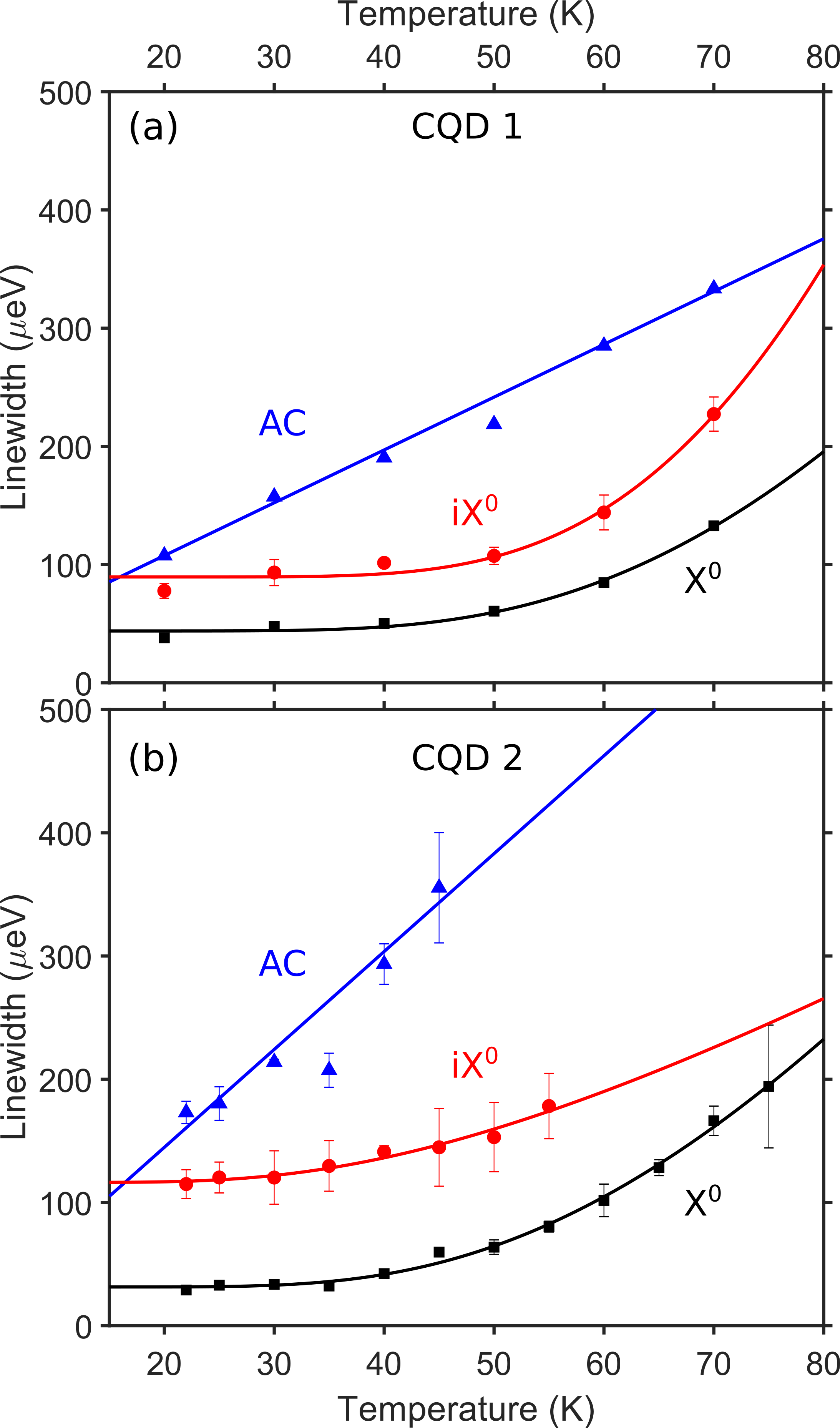

The temperature dependence of the PL linewidth is shown in Fig. 3 for two CQDs on the same sample, with the theoretical dependence given by Eq’s. (12) and (14). At low temperatures, the linewidth is determined by the one-phonon transition rate between the lowest two eigenstates, with the temperature dependence entering through the phonon mode population at the transition frequency. The energy splitting at the anticrossing is significantly smaller than the thermal energy in these measurements, leading to the observed linear broadening for the upper branch
| (1) |
The slope of this linear broadening, measured as eV/K for CQD 1 and eV/K for CQD 2, is therefore proportional to the interdot phonon coupling strength through the spectral density at the transition frequency. The difference in broadening slope and phonon coupling strength between CQD 1 and CQD 2 can be explained by a variation of lateral alignment between QDs, as discussed in Section IV. This explanation is supported by the observation of different tunnel coupling strengths eV and eV of the first two excited states of the neutral exciton in CQD 1, corresponding to coupling between the ground state of the bottom QD and the first two excited states of the top QD with -like orbitals meV and meV above the ground state, respectively.Scheibner et al. (2008) The different energies of the -like and -like excited states indicate an elongated top QD, while the larger tunnel coupling strength of the second excited state indicates a lateral misalignment between QDs along the shorter axis of the top QD. The measurements were limited to a temperature K due to the closed cycle cryostat system used. We expect that the linewidth at the anticrossing would approach a constant value at lower temperatures between K where the thermal energy decreases below the energy splitting.
The effect of energy splitting between exciton branches on the phonon-induced linewidth broadening for 7 CQDs is shown in Fig. 4. The value of phonon broadening for each branch is obtained by fitting the bias-dependent linewidth to Eq. 17 to remove the effects of Gaussian broadening due to charge fluctuations and spectrometer resolution. The results are compared with numerical simulations of perfectly aligned QDs with an interdot barrier width of nm, predicting a maximum broadening of eV at meV for the upper branch and eV at meV for the lower branch. This corresponds to a maximum transition rate of () for phonon emission (absorption). The experimental data appears to follow the simulated curve with variations of up to from predictions using average phonon coupling strength. The inferred transition rates are comparable to measuredMüller et al. (2012, 2013) and calculatedClimente et al. (2006); Gawarecki et al. (2010); Gawarecki and Machnikowski (2012); Daniels et al. (2013) electron/hole interdot relaxation rates in the meV energy range, though substantially lower rates have also been observed.Nakaoka et al. (2006); Wijesundara et al. (2011); Rolon et al. (2012)
III Theoretical Model
To describe the optical transitions of a tunnel-coupled quantum dot pair (CQD) in an electric field-effect diode structure near a resonant tunneling anticrossing, we follow Refs. Daniels et al., 2013 and Gawarecki et al., 2010 by starting with a two-band effective mass model to describe bound charges in the conduction and heavy-hole valence bands. This gives single-particle wavefunctions with band index , QD location , spin state , and lattice-periodic Bloch wavefunctions . The confinement model and resulting envelope wavefunctions are detailed in Appendix A.
Near the ground state hole tunneling resonance of the neutral exciton state, the spatially direct and indirect excitons expressed in the localized basis as and , respectively, are coupled to form new eigenstates
| (2) | ||||
The coefficients are found by diagonalizing the Hamiltonian matrixBayer et al. (2001)
| (3) |
where is the hole tunnel coupling energy and is the experimentally determined energy of state as a function of bias voltage applied to the diode. The eigenstate energies
| (4) | ||||
form an avoided crossing, or anticrossing, with the minimum energy difference at resonance given by . Using the linear approximation of Stark shift near an anticrossing centered at , the eigenstate energies are given by and , leading to the bias-dependent slopes
| (5) |
for each eigenstate.
Coupling between single bound charges and lattice phonons can be described using the general HamiltonianClimente et al. (2006); Gawarecki et al. (2010); Gawarecki and Machnikowski (2012); Daniels et al. (2013)
| (6) | ||||
with creation (annihilation) operators () for phonon modes with polarization and wave vector , () for electrons in state , and () for holes in state . The phonon coupling constants are expanded into bulk and localized contributions as , with bulk coupling matrix elements depending on phonon mode and coupling mechanism and geometric form factors
| (7) |
describing overlap of the envelope wavefunctions of involved states modulated by the phonon mode phase.
Since we are interested in transitions between the two lowest-energy neutral exciton states near a tunneling resonance, the relevant energy differences are less than 15 meV, so coupling to optical phonons at energies of 30-40 meV is neglected. The relevant phonon coupling mechanisms which contribute to the bulk matrix element therefore include deformation potential (DP) coupling to LA phonons, given by
| (8) |
and piezoelectric (PE) coupling to LA and TA phonons, given by
| (9) |
In equations (8) and (9), is the mass density of the crystal, is the crystal volume used for normalization of phonon modes (cancels out after summation over wave vectors), is the propagation velocity of phonon mode , is the deformation potential of the conduction/valence band, is the piezoelectric constant of the crystal, is the electric permittivity of the crystal, and the directional dependence of the PE coupling is detailed in Appendix B. Note that these bulk coupling matrix elements assume a constant value of each material parameter, without taking into account variations in composition due to the CQD structure. Previous studies therefore assume that these parameters are determined entirely by the GaAs barrier material, or by assuming a uniform effective composition.Gawarecki et al. (2010); Daniels et al. (2013)
The single-particle phonon coupling Hamiltonian given by Eq. (6) can be transformed to the diagonalized exciton basis as
| (10) |
where the exciton-phonon coupling constants are obtained by projecting Eq. (6) onto the diagonalized eigenstates. Transitions between states and necessarily involve hole tunneling, such that electron-phonon coupling does not contribute. Pure dephasing processes with no population transfer, describing phonon-assisted optical transitions, can occur by electron- or hole-phonon coupling. Taking these properties into account, the exciton-phonon coupling constants are given in terms of the localized single-particle coupling constants as
| (11) | ||||

The rate of phonon-assisted tunneling transitions from state to state due to first-order coupling is given by Fermi’s golden rule as
| (12) |
where the phonon spectral density
| (13) |
measures the coupling to phonon modes at the transition frequency to ensure energy conservation, the temperature-dependent phonon mode population is given by the Bose distribution , and the step function for phonon absorption (emission).
The general expression for the energy linewidth of each exciton state
| (14) |
contains contributions from real transitions to other states as well as virtual single-state transitions associated with phonon-assisted optical absorption, resulting in acoustic phonon sidebands around the Lorentzian zero-phonon line (ZPL) and pure dephasing.Besombes et al. (2001); Favero et al. (2003); Borri et al. (2003, 2005) Here we consider only the lowest-energy direct and indirect states, neglecting excited states, which are expected to be meV higher in energy and have a negligibly small tunneling rate. The frequency-dependent pure dephasing rate is calculated similarly to the tunneling rate, with the phonon energy determined by the detuning of the optical frequency from resonance:
| (15) |
Experimentally, the emission spectrum is detected using a spectrometer with a finite resolution. As a result, the detected spectrum is convolved with the typically Gaussian spectrometer response function of width (eV in these experiments), leading to a Voigt ZPL profile with phonon sidebands. In the presence of a fluctuating electric field due to many charged lattice defects near the CQD, an additional Gaussian broadening is present, with a width proportional to the bias slope of the transition energy given in Eq. 5. With both of these broadening mechanisms, the combined Gaussian ZPL broadening is given by
| (16) |
IV Discussion
The non-monotonic bias dependence of linewidth in Fig. 2a, together with the additional temperature-dependent broadening in Fig. 3, indicate a significant enhancement of phonon-assisted transition rates between eigenstates at tunneling resonances. The bias-dependent ZPL linewidth can be fit to the predicted form of Gaussian broadening in Eq. 16 with an additional phonon-induced broadening with a Lorentzian shape, resulting in the function
| (17) |
for each branch, with fit parameters , , and describing the position and shape of the anticrossing energy levels and , , and describing the strength of broadening due to charge fluctuations, spectrometer resolution, and phonon-assisted transitions, respectively.


The theory predicts an asymmetry in peak linewidths of the upper and lower branches, with the upper branch being more broad due to a faster phonon emission process compared to phonon absorption, resulting in a shorter lifetime for state . Fits to observed spectra appear to show an additional broadening of the lower branch just past the center of the anticrossing, to a level higher than the peak linewidth of the upper branch. However, the region with increased fit linewidth of the lower branch corresponds to where a second faintly visible peak merges with it. This peak appears to be due to a weakly-allowed recombination from the dark exciton spin state due to spin-orbit coupling, with an exchange splitting of eV far from the anticrossing.Daniels et al. (2013); Doty et al. (2010)
Fig. 5 shows the calculated phonon-assisted transition and pure dephasing rates both on and off the anticrossing resonance for each coupling mechanism at 20 K, as a function of phonon energy. Transitions between eigenstates are dominated by piezoelectric coupling at low energies, with a maximum at meV for phonon absorption from the lower branch. The linewidth broadening effect is therefore predicted to be strongest for CQDs with an anticrossing splitting energy of meV. The sideband-producing pure dephasing process is dominated by deformation potential coupling, with a maximum at 1.2 meV. The experimental spectra should therefore give a measure of piezoelectric coupling strength through the ZPL linewidth at the anticrossing and deformation potential coupling through the intensity and distribution of acoustic phonon sidebands, which are more prominent away from the anticrossing where the ZPL is narrower. The oscillatory decay of transition and dephasing rates as a function of phonon energy is a known feature of CQDs, arising from resonances in the phonon coupling form factor (Eq. 7) between phonon wavelength and QD separation.Climente et al. (2006); Gawarecki et al. (2010); Wijesundara et al. (2011); Rolon et al. (2012) The complex oscillation pattern and its bias dependence are due to the combination of single-particle coupling components between localized basis states, as calculated from Eq. 11. The phonon coupling strength , primarily due to the piezoelectric interaction, was initially too high when calculated using the material parameters for GaAs listed in Table 1. This was reduced to match observed peak anticrossing linewidths by using effective composition values of when calculating phonon coupling constants, with material parameters varying linearly between GaAs () and InAs (). The deformation potential parameters and were both increased by a factor between 1.27 and 2.22 relative to the values listed in Table 1 to match observed sideband intensities between and of ZPL intensity, since literature values of these parameters are highly inconsistent. The resulting values of InAs composition and phonon coupling strength match our experimental observations within the two-band effective mass model and are consistent with reports of In migration during QD growth,Liu et al. (2000); Kegel et al. (2001); Lenz et al. (2002); Jovanov et al. (2012) though inclusion of coupling with light-hole valence bands may significantly modify these values.Climente et al. (2008); Gawarecki and Machnikowski (2012) The coupling strength could also be modified more weakly through the form factor by changing the QD charge confinement and single-particle wavefunctions.
The variations in phonon coupling strength can potentially be explained by differences in CQD geometry throughout the sample, with simulated dependence on interdot barrier width shown in Fig. 6 and on lateral misalignment in Fig. 7. While the interdot barrier width is expected to be quite uniform throughout each sample, variances in CQD alignment have been observed and could significantly reduce the phonon coupling depending on the lateral confinement within each QD.Doty et al. (2010) Since the value of tunnel coupling and anticrossing energy is proportional to wavefunction overlap between localized states, we calibrate the value of anticrossing energy expected in each case using previous measurements on a series of CQD samples grown similarly with different interdot barrier widths to obtain the curves in the lower plots.Bracker et al. (2006) The simulations predict maximum phonon broadening for interdot barrier widths near 4 nm, and a decrease in phonon broadening with lateral QD misalignment.
While the data and simulations presented in this report focus on the hole tunneling resonance of the neutral exciton state, we expect that the enhancement of phonon coupling at tunneling resonances is a more general effect which can apply to different charge states as well. The geometric phonon coupling form factor is increased by the formation of delocalized eigenstates, which occurs at any tunneling resonance regardless of the configuration of resident charges. The bulk PE coupling constant (Eq. 9) is equal for electrons and holes, so the effect can occur regardless of which charge carrier is tunneling. The only remaining requirement for strong phonon coupling enhancement is that the AC splitting energy lies near the maximum of the phonon spectral density for PE coupling, a condition which depends on the size and confinement potential of the QDs. Electron tunneling ACs typically have a much larger energy splitting due to their lower effective mass, inhibiting this effect since PE coupling is strongly weighted towards lower phonon energies.Bracker et al. (2006) The effect might be observed with electron tunneling by reducing AC splitting energy through proper band engineering of the interdot barrierLiu et al. (2011) or by working with excited-state ACs.Scheibner et al. (2008); Müller et al. (2012, 2013) Initial observations indicate a similar level of phonon broadening at hole tunneling resonances in positive trion and neutral biexciton transitions, though the presence of additional optically active spin states makes the fitting procedure more complicated and the results less reliable.
V Conclusion
To conclude, we have measured the linewidths of direct exciton, indirect exciton and tunneling resonance states for CQDs. We find that pure dephasing, phonon relaxation and charge fluctuations in the CQDs can explain the observed linewidth broadening. The existence of phonon transitions between the molecular-like excitons in the system causes the linewidth to broaden beyond the charge fluctuation-induced broadening of the indirect exciton state. The transition of linewidths from direct to indirect exciton state is non-monotonic near tunneling resonances and phonon-induced broadening up to 100 eV is reported at 20 K, corresponding to phonon-assisted transition rates up to . These measurements are in good agreement with theoretical calculations of linewidth broadening at tunneling resonances including phonon-assisted transitions due to PE and DP coupling.
Acknowledgements.
We acknowledge funding from the Defense Threat Reduction Agency (Grant No. HDTRA1-15-1-0011). A.S.B., S.G.C., and D.G. acknowledge the support of Office of Naval Research.Appendix A Single-Particle Wavefunctions
The slowly-varying envelope wavefunctions are solutions to the Schrödinger equation
| (18) |
with effective mass , confinement potential and single-particle confinement energies .
Eq. (18) can be simplified by modeling the confinement potential of each quantum dot (QD) using the cylindrically symmetric function
| (19) |
to describe finite well confinement in the vertical direction due to band-edge offsets of the heterostructure and harmonic oscillator confinement in the lateral direction, where is the Heaviside step function, is the height of the QD, and the angular frequency of the lateral harmonic oscillator is set by the experimentally determined spacing between the ground and first excited states. Eq. (18) is then solved using separation of variables to give envelope wavefunctions of single-particle localized ground states as
| (20) |
where is a normalization constant defined such that and the -component of the wavefunction is expressed as the piecewise function
| (21) |
with wavenumber determined as the -th solution to the transcendental equation
| (22) |
due to the boundary conditions for continuity of the wavefunction and its first derivative,
| (23) |
and . In a coordinate system with the origin set at the center between the two QDs and assuming no lateral misalignment such that cylindrical symmetry is preserved, wavefunctions for particles localized in each dot are found from Eqs. (20) and (21) as , with the substitution to account for the different height of each QD and center-to-center QD separation .
We note that Refs. Daniels et al., 2013 and Gawarecki et al., 2010 use a more detailed geometrical model of the CQD, treating the confinement potential as a pair of lens-shaped finite wells. They use an adiabatic separation of variables technique to solve the 1-D Schrödinger equation with finite double well potential in the vertical direction at each radial distance and use the resulting radius-dependent confinement energy as an additional potential term in the radial Schrödinger equation. Finally, the Ritz variational method is applied to approximate the eigenstates as linear combinations of the obtained vertical and radial wavefunctions which minimize the total energy. Ref. Gawarecki et al., 2010 additionally uses a continuum elasticity model to calculate the strain distribution and obtain spatially-dependent components of the anisotropic effective mass tensor, both of which are used as inputs to the eigenstate calculations.
Appendix B Simulation Methods
For numerical simulations, each integral is converted to a sum over a grid of values with a sufficient number of grid points to achieve satisfactory convergence. Since the system is assumed to have cylindrical symmetry, single-particle localized ground state wavefunctions are calculated using Eq. (20) and represented in cylindrical coordinates as a product of - and -dependent components . Both and values are represented as 100-point grids, covering nm in the direction and nm in the direction. For simulations varying lateral offset between QDs (Fig. 7), wavefunctions are represented in Cartesian coordinates with a 25-point grid in each dimension since cylindrical symmetry is broken. Due to the delta function in Eq. (13) which enforces energy conservation, it is most convenient to express phonon wavevectors in terms of energy in spherical coordinates . Both angular coordinates are represented as 200-point grids covering a full solid angle, with the azimuthal coordinate from to and the polar coordinate from to .
The directional dependence of the PE coupling is given in terms of the phonon mode polarization vectors as
| (24) |
Using the phonon mode polarization vectors
| (25) | ||||
equation (24) for each phonon mode becomes
| (26) | ||||
Due to the cylindrical symmetry, is averaged over the azimuthal coordinate as to obtain
| (27) | ||||
Evaluation of the geometric form factors defined in Eq. (7) involves integration over a three-dimensional grid of spatial coordinates for each value of the phonon wave vector on a separate three-dimensional grid, thereby constituting a major bottleneck in numerical calculations. Ref. Gawarecki et al., 2010 uses the cylindrical symmetry of the envelope wavefunctions to simplify these integrals by separating variables and evaluating the angular integral in terms of ’th-order Bessel functions of the first kind . For the separable ground-state wavefunctions defined in Eq. (20) and phonon wave vectors defined in cylindrical coordinates as , this expression becomes
| (28) | ||||
The form factor is then expressed in spherical coordinates using the transformations and .
Finally, single-particle coupling constants , calculated using the obtained form factors and bulk coupling constants given by Eqs. (8) and (9), are represented for each particle and set of QD locations as a function of phonon mode , phonon energy , and polar angle . The summation over phonon modes is represented in spherical coordinates as an integral over wave vectors with a fixed magnitude:
| (29) | ||||
where the dispersion relation is used to relate wave vector magnitude to the mode-dependent group velocity , and the mode volume cancels with the corresponding factor in the bulk coupling constants .
Ref. Daniels et al., 2013 uses a single-particle Green’s function description of linear susceptibility within the electric dipole and rotating wave approximations to obtain an expression for the optical absorption spectrum as a sum of Lorentzian contributions
| (30) |
where is the optical dipole matrix element of transition . These matrix elements are expressed in terms of electron-hole wavefunction overlaps
| (31) |
of localized exciton states, giving
| (32) | ||||
The optical emission spectrum is also calculated similarly to the absorption spectrum, with only the pure dephasing rates modified by changing the sign of detuning terms to to reflect the reversal of phonon absorption and emission processes.
At each value of the bias voltage , the tunneling Hamiltonian given by Eq. (3) is diagonalized to obtain the eigenstate coefficients . These are used to obtain the phonon coupling constants and optical dipole matrix elements in the eigenstate basis. The phonon spectral density can then be calculated using Eq. (29), allowing calculation of the optical transition rates and absorption and emission spectra using Eq. (30). As a final step, Gaussian convolutions are applied to the optical transition spectra in the energy and bias directions to reproduce broadening due to the spectrometer response and local charge fluctuations, respectively. The values of material and structural parameters used in the simulations are listed in Table 1, except where otherwise noted.
Appendix C Parameter Values
| GaAs | InAs | ||
| Material Parameters | |||
| Electron effective mass () Barker and O’Reilly (2000) | 0.059 | 0.042 | |
| Hole effective mass () Barker and O’Reilly (2000) | 0.37 | 0.34 | |
| Conduction band edge (eV) Barker and O’Reilly (2000) | 1.518 | 1.057 | |
| Valence band edge (eV) Barker and O’Reilly (2000) | 0 | 0.192 | |
| CB deformation potential (eV) Gawarecki et al. (2010) | -9.3 | ||
| VB deformation potential (eV) Gawarecki et al. (2010) | -0.7 | ||
| Piezoelectric constant () Gawarecki et al. (2010) | 0.16 | 0.045 | |
| Relative dielectric constant Gawarecki et al. (2010) | 12.9 | 15.15 | |
| Crystal density () Gawarecki et al. (2010) | 5300 | 5670 | |
| LA phonon velocity (m/s) Gawarecki et al. (2010) | 5150 | ||
| TA phonon velocity (m/s) Gawarecki et al. (2010) | 2800 | ||
| Quantum Dot Parameters | |||
| Bottom QD height (nm) Scheibner et al. (2008) | 2.9 | ||
| Top QD height (nm) Scheibner et al. (2008) | 2.1 | ||
| QD center separation (nm) | 6.5 | ||
| excited state spacing (meV) | 100 | ||
| excited state spacing (meV) Scheibner et al. (2008) | 21.2 | ||
| tunnel coupling () | 330.5 | ||
| Exciton intensity ratio | 17.09 | ||
| Bias fluctuation width (mV) | 3.58 | ||
| Experiment Parameters | |||
| Temperature (K) | 20 | ||
| Spectrometer resolution () | 37.0 | ||
References
- Ramanathan et al. (2013) S. Ramanathan, G. Petersen, K. Wijesundara, R. Thota, E. Stinaff, M. Kerfoot, M. Scheibner, A. Bracker, and D. Gammon, App. Phys. Lett. 102, 213101 (2013).
- Scheibner et al. (2009) M. Scheibner, A. S. Bracker, D. Kim, and D. Gammon, Solid State Commun. 149, 1427 (2009).
- Stinaff et al. (2006) E. A. Stinaff, M. Scheibner, A. S. Bracker, I. V. Ponomarev, V. L. Korenev, M. E. Ware, M. F. Doty, T. L. Reinecke, and D. Gammon, Science 311, 636 (2006).
- Jennings et al. (2019) C. Jennings, X. Ma, T. Wickramasinghe, M. Doty, M. Scheibner, E. Stinaff, and M. Ware, Adv. Quantum Tech. 3, 1900085 (2019).
- Kim et al. (2011) D. Kim, S. G. Carter, A. Greilich, A. S. Bracker, and D. Gammon, Nature Phys. 7, 223 (2011).
- Loss and DiVincenzo (1998) D. Loss and D. P. DiVincenzo, Phys. Rev. A 57, 120 (1998).
- Scheibner et al. (2012) M. Scheibner, S. Economou, A. Bracker, D. Gammon, and I. Ponomarev, J. Opt. Soc. Am. B 29, A82 (2012).
- Gao et al. (2012) W. Gao, P. Fallahi, E. Togan, J. Miguel-Sanchez, and A. Imamoglu, Nature 491, 426 (2012).
- Vora et al. (2015) P. M. Vora, A. S. Bracker, S. G. Carter, T. M. Sweener, M. Kim, C. S. Kim, L. Yang, P. G. Brereton, S. E. Economou, and D. Gammon, Nat. Commun. 6, 7665 (2015).
- Knill et al. (2001) E. Knill, R. Laflamme, and G. J. Millburn, Nature 409, 46 (2001).
- Bayer et al. (2001) M. Bayer, P. Hawrylak, K. Hinzer, S. Fafard, M. Korkusinski, Z. R. Wasilewski, O. Stern, and A. Forchel, Science 291, 451 (2001).
- Borri et al. (2003) P. Borri, W. Langbein, U. Woggon, M. Schwab, M. Bayer, S. Fafard, Z. Wasilewski, and P. Hawrylak, Phys. Rev. Lett. 91, 267401 (2003).
- Muljarov et al. (2005) E. A. Muljarov, T. Takagahara, and R. Zimmermann, Phys. Rev. Lett. 95, 177405 (2005).
- Bardot et al. (2005) C. Bardot, M. Schwab, M. Bayer, S. Fafard, Z. Wasilewski, and P. Hawrylak, Phys. Rev. B 72, 035314 (2005).
- Climente et al. (2006) J. I. Climente, A. Bertoni, G. Goldoni, and E. Molinari, Phys. Rev. B 74, 035313 (2006).
- Nakaoka et al. (2006) T. Nakaoka, E. C. Clark, H. J. Krenner, M. Sabathil, M. Bichler, Y. Arakawa, G. Abstreiter, and J. J. Finley, Phys. Rev. B 74, 121305(R) (2006).
- Gawarecki et al. (2010) K. Gawarecki, M. Pochwala, A. Grodecka-Grad, and P. Machnikowski, Phys. Rev. B 81, 245312 (2010).
- Gawarecki and Machnikowski (2012) K. Gawarecki and P. Machnikowski, Phys. Rev. B 85, 041305(R) (2012).
- Wijesundara et al. (2011) K. C. Wijesundara, J. E. Rolon, S. E. Ulloa, A. S. Bracker, D. Gammon, and E. A. Stinaff, Phys. Rev. B 84, 081404(R) (2011).
- Rolon et al. (2012) J. Rolon, K. Wijesundara, S. Ulloa, A. Bracker, D. Gammon, and E. Stinaff, J. Opt. Soc. Am. B 29, A146 (2012).
- Müller et al. (2012) K. Müller, A. Bechtold, C. Ruppert, M. Zecherle, G. Reithmaier, M. Bichler, H. J. Krenner, G. Abstreiter, A. W. Holleitner, J. M. Villas-Boas, et al., Phys. Rev. Lett. 108, 197402 (2012).
- Müller et al. (2013) K. Müller, A. Bechtold, C. Ruppert, T. Kaldewey, M. Zecherle, J. S. Wildmann, M. Bichler, H. J. Krenner, J. M. Villas-Boas, G. Abstreiter, et al., Ann. Phys. (Berl.) 525, 49 (2013).
- Daniels et al. (2013) J. M. Daniels, P. Machnikowski, and T. Kuhn, Phys. Rev. B 88, 205307 (2013).
- Ha et al. (2015) N. Ha, T. Mano, Y.-L. Chou, Y.-N. Wu, S.-J. Cheng, J. Bocquel, P. M. Koenraad, A. Ohtake, Y. Sakuma, K. Sakoda, et al., Phys. Rev. B 92, 075306 (2015).
- Zhou et al. (2013) X. R. Zhou, J. H. Lee, G. J. Salamo, M. Royo, J. I. Climente, and M. F. Doty, Phys. Rev. B 87, 125309 (2013).
- Kerfoot et al. (2014) M. Kerfoot, A. Govorov, C. Czarnocki, D. Lu, Y. Gad, A. Bracker, D. Gammon, and M. Scheibner, Nat. Commun. 5, 3299 (2014).
- Scheibner et al. (2008) M. Scheibner, M. Yakes, A. Bracker, I. Ponomarev, M. Doty, C. Hellberg, L. Whitman, T. Reinecke, and D. Gammon, Nat. Phys. 4, 291 (2008).
- Doty et al. (2009) M. F. Doty, J. I. Climente, M. Korkusinski, M. Scheibner, A. S. Bracker, P. Hawrylak, and D. Gammon, Phys. Rev. Lett. 102, 047401 (2009).
- Czarnocki et al. (2016) C. Czarnocki, M. L. Kerfoot, J. Casara, A. R. Jacobs, C. Jennings, and M. Scheibner, J. Vis. Exp. 112, e53719 (2016).
- Besombes et al. (2001) L. Besombes, K. Kheng, L. Marsal, and H. Mariette, Phys. Rev. B 63, 155307 (2001).
- Favero et al. (2003) I. Favero, G. Cassabois, R. Ferreira, D. Darson, C. Voisin, J. Tignon, C. Delalande, G. Bastard, P. Roussignol, and J. M. Gérard, Phys. Rev. B 68, 233301 (2003).
- Borri et al. (2005) P. Borri, W. Langbein, U. Woggon, V. Stavarache, D. Reuter, and A. D. Wieck, Phys. Rev. B 71, 115328 (2005).
- Bracker et al. (2006) A. Bracker, M. Scheibner, M. Doty, E. Stinaff, I. Ponomarev, J. Kim, L. Whitnam, T. Reinecke, and D. Gammon, Appl. Phys. Lett. 89, 233110 (2006).
- Doty et al. (2010) M. F. Doty, J. I. Climente, A. Greilich, M. Yakes, A. S. Bracker, and D. Gammon, Phys. Rev. B 81, 035308 (2010).
- Liu et al. (2000) N. Liu, J. Tersoff, O. Baklenov, A. L. Holmes, and C. K. Shih, Phys. Rev. Lett. 84, 334 (2000).
- Kegel et al. (2001) I. Kegel, T. H. Metzger, A. Lorke, J. Peisl, J. Stangl, G. Bauer, K. Nordlund, W. V. Schoenfeld, and P. M. Petroff, Phys. Rev. B 63, 035318 (2001).
- Lenz et al. (2002) A. Lenz, R. Timm, C. Eisele, S. K. Becker, R. L. Sellin, U. W. Pohl, D. Bimberg, and M. Dähne, Appl. Phys. Lett. 81, 5150 (2002).
- Jovanov et al. (2012) V. Jovanov, T. Eissfeller, S. Kapfinger, E. C. Clark, F. Klotz, M. Bichler, J. G. Keizer, P. M. Koenraad, M. S. Brandt, G. Abstreiter, and J. J. Finley, Phys. Rev. B 85, 165433 (2012).
- Climente et al. (2008) J. I. Climente, M. Korkusinski, G. Goldoni, and P. Hawrylak, Phys. Rev. B 78, 115323 (2008).
- Liu et al. (2011) W. Liu, S. Sanwlani, R. Hazbun, J. Kolodzey, A. S. Bracker, D. Gammon, and M. F. Doty, Phys. Rev. B 84, 121304(R) (2011).
- Barker and O’Reilly (2000) J. A. Barker and E. P. O’Reilly, Phys. Rev. B 61, 13840 (2000).