SliT: A strip-sensor readout chip
with subnanosecond time walk
for the J-PARC muon /EDM experiment
Abstract
A new silicon-strip readout chip named “SliT” has been developed for the measurement of the muon anomalous magnetic moment and electric dipole moment at J-PARC. The SliT chip is designed in the Silterra 180 nm CMOS technology with mixed-signal integrated circuits. An analog circuit incorporates a conventional charge-sensitive amplifier, shaping amplifiers, and two distinct discriminators for each of the 128 identical channels. A digital part includes storage memories, an event building block, a serializer, and LVDS drivers. A distinct feature of the SliT is utilization of the zero-crossing architecture, which consists of a CR-RC filter followed by a CR circuit as a voltage differentiator. This architecture allows generating hit signals with subnanosecond amplitude-independent time walk, which is the primary requirement for the experiment. The test results show a time walk of ns between 0.5 and 3 MIP signals. The equivalent noise charge is (rms) at pF as a strip-sensor capacitance. The SliT128C satisfies all requirements of the J-PARC muon /EDM experiment.
Index Terms:
silicon-strip, CMOS, ASIC, time walk, low-noise, J-PARC, Muon, , EDMI Introduction
The anomalous magnetic moment () and the electric dipole moment (EDM) of the muon are sensitive probes of new physics beyond the Standard Model (SM). The SM is a well-tested physics theory, however, there exists a discrepancy in the muon between the SM prediction [1, 2] and its most precise measurement by the E821 collaboration at Brookhaven National Laboratory (BNL) by more than three standard deviations [3]. An experiment to improve the precision of the muon is ongoing at Fermilab which uses the upgraded apparatus and plans to increase statistics [4]. On the other hand, another measurement of the muon /EDM is currently under preparation based on a different experimental approach to make a definitive conclusion. This experiment applies an innovative technique using a reaccelerated thermal muon beam at the Japan Proton Accelerator Research Complex (J-PARC) [5].
A primary goal of the experiment is to measure the muon with a precision of 0.1 parts per million (ppm), which corresponds to an improvement by a factor of five compared to the BNL experiment. At the same time, we seek for the muon EDM with a sensitivity of cm. The reaccelerated thermal muon beam with a repetition rate of 25 Hz to be used at J-PARC is produced from a thermal muonium source, followed by laser ionization and acceleration. The reaccelerated muons with a momentum of 300 MeV/ are stored under a 3 T magnetic field. The muon makes the orbital cyclotron motion in the mid-plane of the muon storage magnet. A positron tracking detector is placed in the innner region of the muon storage ring for the detection of positrons from the muon decay, i.e., . Fig. 1 shows the concept of the muon storage ring and positron detector in the experiment. The 40 sensor vanes are aligned radially in the detection volume. Each vane consists of single-sided p-on-n type silicon-strip sensors [6] with mutually orthogonal strips on both sides. A two-dimensional position of a positron track is therefore determined by two layers of the strip sensors. Circular positron tracks are reconstructed by connecting two-dimensional positions and their momenta are derived from the curvature. To maximize the statistical sensitivity of the muon , we will use the positron tracks with a momentum in the range from 200 MeV/ to 275 MeV/ for the analysis. The measurement will be performed in an interval following a fill of 33 s, which is five times longer than the lifetime of the muon with the momentum of 300 MeV/.
An integrated circuit with a fast response and high granularity is used to readout data from the silicon strip detectors. The integrated circuit is equipped with a deep buffer memory to store the data for a beam spill. The stored data is readout before the next beam bunch coming. To meet the experimental requirements, a series of custom front-end readout chips named “SliT” has been developed in 180 nm CMOS technology. We have newly developed a full channel chip named “SliT128C”, and its performance has been tested in the laboratory. In this paper, we describe the ASIC (application-specific integrated circuit) design in section II, report the evaluation setup and the performance test results in section III, and finally give conclusions in section IV.
II Architecture of the ASIC
II-A Experimental requirements and developmental background
The readout ASIC was implemented in the Silterra 180 nm CMOS technology. Table I summarizes the technological parameters. The front-end ASICs for silicon-strip sensors are requested to tolerate a high hit rate up to 1.4 MHz per strip with a stability to dynamically changing hit rates by a factor of 150 from the beginning to the end of measurements. In order to minimize the pileups, a pulse width for a typical minimum-ionizing particle (MIP) signal has to be smaller than 100 ns. Here, the pulse width is defined from a 1 MIP output, which intersects a threshold set at 0.3 MIP. For the further reduction of the pileups and precise detection of circular positron tracks from the muon decays, a subnanosecond time walk is of critical importance in analog processing blocks of the readout ASIC. The experimental requirements translated to concrete circuit specifications are summarized in Table II.
AC-coupled single-sided p-on-n type silicon-strip sensors with a double-metal structure were made by Hamamatsu Photonics K.K. [6]. The sensor thickness is 320 m. In this paper, the most probable value of the MIP charge is defined as 3.84 fC, which corresponds to an input charge of about 24,000 . The sensor capacitance is approximately 17 pF, and the total detector capacitance seen from an input of the ASIC is estimated to be less than 30 pF. This value includes the parasitic capacitance coming from Flexible Printed Circuits (FPCs) [7], which connect strip sensors with ASICs. Since the maximum wiring length inside the FPCs is about 250 mm, the parasitic capacitance from the FPCs is not negligible. The equivalent noise charge (ENC) of less than 1600 e- at pF is required.
In the previous studies, we started from a small-scale analog prototype in Silterra 180 nm CMOS technology. Then we fabricated module-prototype chips named “SliT128A” [8] and “SliT128B” [9]. The module-prototype ASICs included 128 readout channels, buffer memories, and other digital processing circuits to store and cope with timing information from the strip sensors. Since the time walk performance was measured as 17.2 ns in SliT128A, we introduced an additional CR block after the semi-Gaussian band-pass filter in SliT128B (see the next section for detailed description of this measure). As a result, the time walk improved to 2 ns, however, it was still larger than the requirement. A new readout chip named “SliT128C” improves the overall analog performance, e.g., the ENC, time walk, and jitter, by optimizing transistor parameters of bias circuits in SliT128B.
Fig. 2 shows the photograph of SliT128C. Inputs of 128 channels are aligned in staggered pads with a pitch of 100 m. The incident signals are processed from the left analog block to the right digital block. Power supply is provided from the top and bottom pads only, and digital outputs are accessed on the right-hand side. To suppress the digital cross talks, the analog and digital blocks are enclosed in distinct deep N-well islands.
| Technology | Silterra 180 nm CMOS, 6 metals |
| Process options | Deep NWell, MIM cap. (4 fF/m2) |
| high resistive p+ poly (1050 /sq.) | |
| Chip size | 6.54 mm 7.2 mm |
| Thickness | 381 m |
| Supply rail | 1.8 V (core/IO) |
II-B Analog processing block
Fig. 3 shows the signal processing chain of each channel. The strip sensor is AC-coupled to an input of the charge-sensitive amplifier (CSA), while test pulses can be injected via an AC-coupling capacitor of 100 fF. The CSA is based on a folded cascade configuration with a p-channel input transistor (m nm). In terms of noise performance, we increased the folding number of the input transistor to , which are placed in parallel. The feedback capacitor was implemented by a metal-insulator-metal structure with a value of 170 fF. A transfer gate type FET was employed for the CSA DC-feedback component.
The CSA output is fed into a CR-RC shaping amplifier composed of a pole-zero cancellation circuit (PZC) and a second-order integration low-pass filter. The capacitors and resistance values in the PZC were selected to meet the equation of . In the semi-Gaussian shaper, high-resistance p+ poly-silicons were chosen as resistors. Strictly speaking, the parameters of and have to meet the equation of for the ideal case that the network functions as the second-order CR-RC shaper [10], however, we have tuned the actual values to minimize time walks by a SPICE simulation.
The shaper output is amplified by an inverting amplifier by a factor of two. This function is selectable with a CMOS switch on the outside chance that voltage slopes of the shaper output affect timing accuracy. After the inverting amplifier, the output is fed into two signal paths, one of which is buffered and connected to a discriminator. Baseline tuning is required to adjust the thresholds that is performed by two sets of 7-bit current DACs and resistors. The other signal path is connected to the additional CR circuit, which functions as a voltage differentiator.
In the previous chip, SliT128A, the hit timing was produced from the first-order CR-RC shaper with a peaking time of 50 ns and a single discriminator. This method, however, was not able to reduce the time walk of the discriminator rising edge below the requirement of 1 ns, even after the fine tuning of the threshold. By implementing the differentiator after the CR-RC shaper, we improved the time walks between 0.5 and 3 MIP signals. By differentiating the semi-Gaussian shape, the output shape becomes bipolar, which traverses the baseline given by in Fig. 3. The traversing timing becomes independent of input charges. This method corresponds to the so-called “zero-crossing” architecture and the traversing timing locates at a peaking time of the preceding CR-RC filter. As a result, the discriminator rising edge from the differentiator path remains less than ns, and at the same time, the time walk can be considerably improved.
The noise level after the voltage differentiator becomes worse than the ENC of the CR-RC shaper. To suppress triggers on noise, we preserved the CR-RC shaper path and used both information to define the final pulses by making an AND operation. The leading-edge timing of the final output is determined from the differentiator, while the trailing-edge timing is determined from the CR-RC shaper. Precisely speaking, the noise bandwidths of the CR-RC and CR-RC-CR are theoretically the same, i.e., the differentiator introduces a low-frequency cutoff, whereas the upper cutoff frequency remains about the same [11]. The noise level is related with the reduction in peak amplitude of the bipolar shapes. This degraded slope also produces larger time jitter (not the time walk itself), compared with the CR-RC filter. The time jitter or temperature effect on the time walk is, however, averaged due to large event statistics and not a severe problem in our experiment. The time walk and time jitter estimated by the Monte Carlo simulation, including the device mismatch and parasitic effect, are listed in Table II.
The monitor lines were also implemented to examine analog waveforms at each processing point, e.g., the CSA, CR-RC shaper, differentiator etc. The 20-bit control registers are implemented to enable switches, i.e., a test pulse injection, the inverting amplifier, distinct discriminators, monitor lines, and tuning DACs for each channel.
II-C Digital processing block
Fig. 4 (a) shows the block diagram of the digital part. It consists of a signal interface (I/F), a memory controller, a serializer, a timing generator, and a parameter controller. The timing generator block provides the “Write Start” and “Read Start” signals to the memory controller, which are synchronized with an external 200 MHz clock. The parameter controller block is a slow control circuit for the registers of both the analog and digital parts. The signal interface block receives the discriminator outputs from the analog part. D-type flip-flops sample these signals by the external 200 MHz clock. After the first flip-flops, subsequent two D-type flip-flops resample these signals by 100 MHz clocks which are 180 degrees out of phase. This is because the sampling frequency of 200 MHz is close to the maximum clock frequency of logic circuits in the Silterra technology.
Fig. 4(b) shows the block diagram of the memory controller. The memory controller block receives two kinds of data, which are synchronized by different 100 MHz clocks, from the signal I/F block. When the memory-write controller block receives the “Write Start” signal, it starts to store data in SRAMs. The memories have 8192 word depths for each channel, and the data can be stored within 40.96 s ( ns). The storing process continues until the SRAMs are full. When the memory-read controller block receives the “Read Start” signal, it reads out all of the data from memories and sends them to the serializer block. The data is then sent out by the LVDS drivers with a 50 MHz clock. The data are synchronized by the same 50 MHz clock in the backend electronics, e.g., an FPGA board in our applications, with the DDR (Double Data Rate) mode.
III Performance Tests
III-A Experimental setup
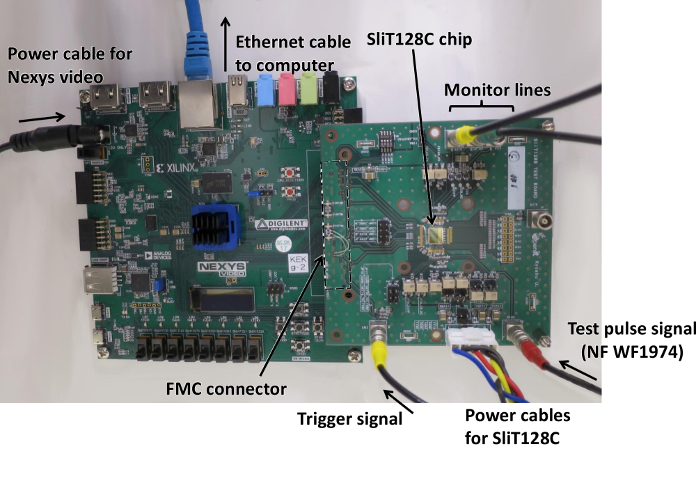
The performance of the SliT128C was evaluated with a test pulse from a function generator. A dedicated printed circuit board (PCB) was designed for performance testing. Fig. 5 shows the experimental setup. A bare die is directly mounted on the PCB and a light-shielding box is placed on the chip. The PCB is electrically connected to the ASIC by 25 m-diameter aluminum wires, and also connected with a commercial field programmable gate array (FPGA) board. We chose the Digilent Nexys Video [12] as an interface with a computer, which is a commercial rigid PCB with a Xilinx Artix-7 FPGA (XC7A200T). This FPGA board provides an easy-to-use programming environment and allows easy modifications to test logics. To store all data from SliT128C, a FIFO is programmed in the FPGA. The stored data are transferred to a computer via an Ethernet cable with the SiTCP protocol [13]. We evaluated the analog performance of 32 out of 128 readout channels, each of which was equipped with 33 pF as a pseudo-strip-sensor capacitance for the test.
III-B Analog waveform and dynamic range
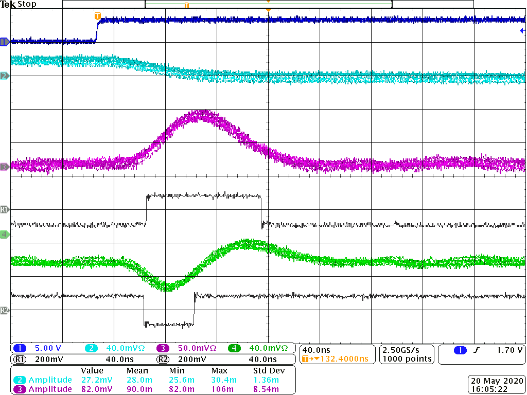
The response of the monitor outputs was investigated to evaluate the analog waveform and dynamic range. Fig. 6 shows typical analog output signals, when a test pulse with 1 MIP charge was injected. The outputs of discriminators are superimposed in black. All monitor lines are functioning as designed. The peaking time and pulse width were 64.2 ns and 99.2 ns, respectively. Comparing with the values from a SPICE simulation (35.1 ns and 75 ns) as shown in Table II, we observe larger values due to a finite output-buffer performance to drive a large capacitive load of the bonding wire, 5 cm microstrips on the PCB, and the probe capacitance of 3.9 pF. The actual pulse width at the discriminator must be shorter than the monitor values, and can be estimated only from the discriminator pulse width described in the following section.
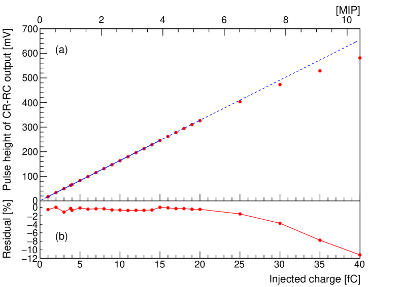
Fig. 7 shows a pulse height of the CR-RC output as a function of injected charges. The wide dynamic range is needed to avoid the saturation for the high hit-rate environment. The integrated non-linearity (INL) was measured as less than 1% and 3.8% in the ranges from 1.92 fC to 20 fC and from 1.92 fC to 30 fC, respectively. An INL of 5% is sufficient for our application. The corresponding dynamic range is larger than 7.8 MIP. We also confirmed that the channel-to-channel variation of offset voltages is within the amplitude of a 1.5 MIP charge that is reasonable to be compensated by 7-bit DACs.
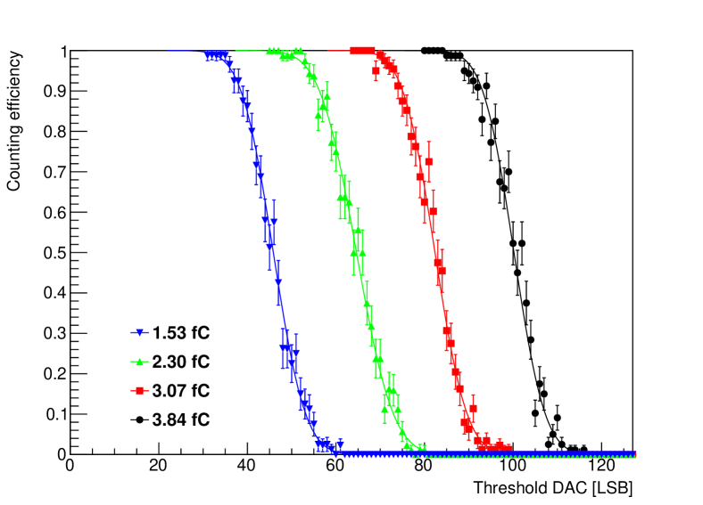
III-C S-curve scan and equivalent noise charge
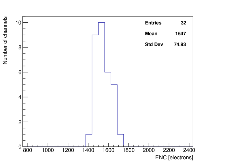
The noise performance was evaluated by scanning the threshold with different injected charges (s-curve scan). First, we enabled only the discriminator in the CR-RC filter, and performed the threshold scans. Fig. 8 shows a counting efficiency as a function of the threshold DAC, a so-called s-curve for a typical channel. The counting efficiency was calculated from the digital outputs. By fitting a complementary error function, i.e., integrated Gaussian function, to the data, the center value and the standard deviation of the Gaussian function are obtained. The center value corresponds to the pulse height. The standard deviation indicates the noise level. One least significant bit (LSB) step size of the threshold DAC for the CR-RC shaper is equivalent to the input charge of 0.043 fC. We repeated this measurement for 32 readout channels, and plot the ENC distribution in Fig. 9. The average equivalent noise charge is measured to be electrons at pF, where the uncertainty indicates the channel-to-channel variation. If we assume the simulated ENC dependence on the detector capacitance (31 electrons/pF), we obtain the ENC to be 1454 electrons at pF, which satisfies the requirement for the noise performance. The simulated ENC is electrons at pF. The ENC difference between the measurement and the simulation can arise due to various factors: parasitic input capacitance, digital crosstalk, and noise injection from the power supplies.
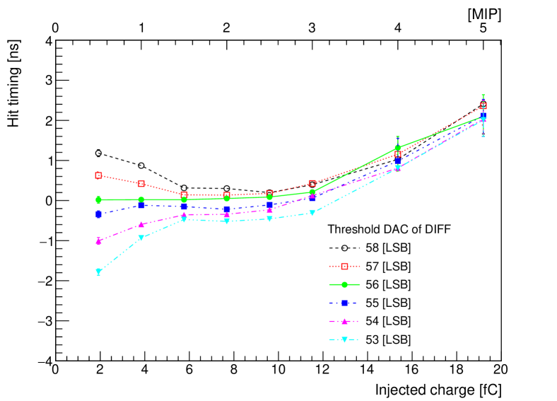
III-D Time walk
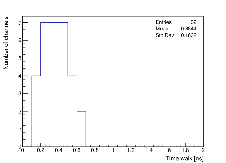
Based on the above results, we set the threshold voltage of the CR-RC shaper to match 1.53 fC which corresponds to an 0.3 MIP charge level in each channel. Then the threshold voltage for the voltage differentiator was adjusted to minimize the time walk. Fig. 10 shows the hit timing vs. threshold voltages of the voltage differentiator in a typical readout channel. The hit timing is defined as the leading-edge timing of the final output, which is determined by the differentiator. A plateau appeared in the hit timing by giving a proper threshold voltage to the differentiator. The time walk of our application is defined as a maximum timing variation in the range from 0.5 MIP to 3.0 MIP. Fig. 11 shows the time walk distribution for the 32 readout channels. This result satisfies the requirement for the time walk and the mean value of the time walk was ns, where the uncertainty indicates the channel-to-channel variation. We note that the hit timing over the injected charges of 3 MIP is increasing, however, we confirmed the plateau can be expanded up to 5 MIP by further tuning the bias of the shaping amplifiers.
III-E Time over threshold and timing jitter
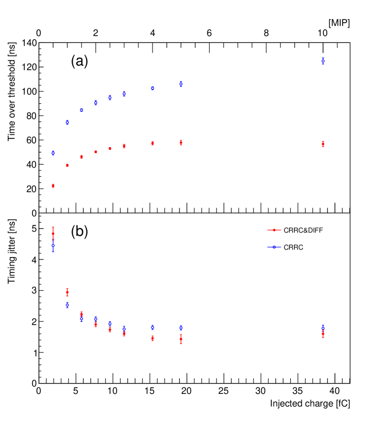
The time over threshold (ToT) as a function of injected charge is shown in Fig. 12(a). The reconstruction quality of the positron tracks can be improved by filtering events based on the ToT information. As described in section II, the leading edge of the hit signal is determined either from the voltage differentiator or the single CR-RC shaper by the register setting. We compared the performance at the normal operating conditions, i.e., using outputs from both CR-RC and voltage differentiator in discriminators, in the case that the CR-RC path only is used to get the ToT values. Both cases are labeled as CRRC&DIFF (red) and CRRC (blue) in the figure. Averaged ToT of 32 channels at 1 MIP are determined as ns (CRRC&DIFF) and ns (CRRC).
We note that the ToT value at 1 MIP of the CRRC case (74.5 ns) can be compared with the simulation value of the pulse width (75 ns) as shown in Table II. The measurement results are close to the designed performance. The ToT of the CRRC&DIFF becomes flat above 15 fC. The non-saturation region can be expanded up to 20 fC by tuning the bias of the shaping amplifiers.
Fig. 12(b) shows the timing jitter () as a function of the injected charge. The timing jitter becomes worse for smaller signals, since the leading edge of the hit signal is directly affected by the electrical noise. The average timing jitter at 1 MIP for 32 channels is ns for the CRRC& DIFF case and ns for the CRRC case. The jitters at 0.5 MIP is ns for the CRRC & DIFF, and ns for the CRRC. They are comparable with the sampling interval of 5 ns.
| Requirement | Simulation | Measurement | |
|---|---|---|---|
| Peaking time | ns | 35.1 ns | 64.2 nsa |
| Pulse width at 1 MIP | ns | 75.0 ns | 74.5 ns |
| Dynamic range | MIP | 8 MIP | MIP |
| ENC | @ pF | 1210 @ pF | @ pF |
| Time walk (0.5-3.0 MIP) | ns | 0.4 ns | ns |
| Jitter at 0.5 MIP | ns | 4.89 ns | ns |
| Power consumption | 0.64 W/chip | N.A. | 0.30 W/chip |
-
a
Outputs measured from the monitor which include delays due to the parasitic capacitance and finite buffer drive strength.
When the number of fired channels are increased, the instantaneous IR drop becomes a main issue to degrade the timing performance. This issue is related with the implementation of decoupling capacitors between supply powers and ground. In our application, the fired channels are estimated to be a few dozen channels at most, and thus, the performance degradation can be negligible in our application.
III-F Power consumption
We supplied 1.8 V for an analog circuit and 1.8 V for a digital one. An additional dedicated bias voltage of 1.1 V is applied to the input transistors in the CSA for noise optimization and avoiding IR-drops. By measuring the current at each power line, power consumption was determined to be 0.13 W, 0.11 W, and 0.06 W for the analog, the digital, and the CSA, respectively. The total power consumption is 0.30 W per chip.
IV Conclusions
We have developed a series of silicon-strip readout chips named SliT with the 180 nm CMOS technology. The SliT is designed for the precise measurement of the muon /EDM, which is planned at J-PARC in Japan. The main objective of the SliT is to provide the timing information for positron tracks from silicon-strip sensors, with amplitude-independent time walks. We have also developed a new readout chip named “SliT128C”. In this chip, the leading edge is generated from the timing of baseline-crossing by the bipolar waveforms. This zero-crossing architecture is implemented by adding the voltage differentiator at the output of the CR-RC shaper. As a result, the time walk effect is suppressed to subnanosecond ( ns). The equivalent noise charge is with pF. The SliT128C consists of 128 channels, which are completely functional. Other evaluated performance results are also summarized in Table II. The SliT128C satisfies all requirements of the J-PARC muon /EDM experiment.
Acknowledgment
The authors would like to thank O. Sasaki, H. Ikeda, and M. Miyahara for constructive comments and useful discussions concerning the design of SliT. The authors also wish to thank the Open Source Consortium of Instrumentation (Open-It) of KEK. This work was supported by the JSPS KAKENHI (Grant No. JP15H05742 and JP18H05226) and the 37th CASIO research funding program (Grant No. 26).
References
- [1] A. Keshavarzi, D. Nomura and T. Teubner, Phys. Rev. D 101, 014029 (2020).
- [2] M. Davier, A. Hoecker, B. Malaescu and Z. Zhang, Eur. Phys. J. C 80, 241 (2020).
- [3] G. W. Bennett et al. [Muon g-2 Collaboration], Phys. Rev. D 73, 072003 (2006).
- [4] J. Grange et al. [Muon g-2], arXiv:1501.06858 [physics.ins-det].
- [5] M. Abe et al., PTEP 2019, 053C02 (2019)
- [6] Hamamatsu Photonics K.K. (available at: https://www.hamamatsu.com/us/en/product/type/S13804/index.html)
- [7] T. Yamanaka et al., Nucl. Instrum. Meth. A 958, 162786 (2020).
- [8] T. Aoyagi et al., JINST 15, P04027 (2020).
- [9] Y. Sato et al., Nucl. Instrum. Meth. A 969, 164035 (2020).
- [10] T. Kishishita et al., IEEE TNS. 57, 15 (2010).
- [11] H. Spieler, “Semiconductor Detector Systems”, Oxford University Press.
- [12] Digilent Nexys Video (available at: https://reference.digilentinc.com/reference/programmable-logic/nexys-video/start)
- [13] T. Uchida, IEEE TNS. 55, 3 (2008).