Sliding ferroelectricity in a bulk misfit layer compound (PbS)1.18VS2
Abstract
Twisted heterostructures of two-dimensional crystals can create a moiré landscape, which can change the properties of it’s parent crystals. However,the reproducibility of manual stacking is far from perfect. Here, the alternated stacking of post-transition metal monochalcogenides and transition metal dichalcogenides in misfit layer compound crystals is used as a moiré generator. Using X-ray diffraction, the presence of twins with a well-defined small twist angle between them is shown. Due to the twist, the surface electrical potential from the induced ferroelectricity is observed using scanning probe microscopy and electron microscopy.
The group of possible two-dimensional (2D) ferroelectric materials has been significantly expanded by the recent theoretical prediction [1, 2, 3, 4] and experimental confirmation [5, 6, 7, 8, 9, 10] of sliding ferroelectricity. For certain stacking configurations in bi- and multilayer 2D materials, the inversion and/or mirror symmetry is broken and thereby an in- and/or out-of-plane polarization are induced. Due to the weak interlayer interaction in van der Waals multilayers, the polarization can be reversed via in-plane lattice sliding.
Experimentally, a sliding ferroelectric material can be created by manual stacking of 2D van der Waals materials on top of each other with a defined twist angle [11, 12, 13, 14]. Unfortunately, manual stacking can create difficulties with device reproducibility [15]. Sliding ferroelectricity can also be observed in bulk van der Waals crystals, as long as there is no inversion symmetry between the layers, as was recently shown for the amphidynamic crystal (15-crown-5)Cd3Cl6 [16]. In the case of transition metal dichalcogenides (TMD) crystals, the centrosymmetric 2H-form is the most common stable form and rarely a 3R-stacked bilayer can be found [14]. Nevertheless, bulk crystals with a broken inversion symmetry can be grown, such as 3R-MoS2 [17] or graphene polytypes with stacking faults or twins [4, 10]. Also in van der Waals epitaxy of 2D materials on (quasi)-2D substrates, the formation of stacking faults and twins is often observed, due to very similar binding energies for the different stacking configurations [18].
In this work, instead of manually stacking a van der Waals heterostructure with a certain twist angle, we searched for a class of 2D materials where twins having a small twist angle with respect to each other can be easily induced during the growth. A member of the TMD class are the misfit layer compounds (MLCs) with the general formula (MX)1+m(TX2)n, where M = Sn, Pb, Sb, Bi, or a rare earth element; T = Ti, V, Cr, Nb, or Ta; X = S, or Se; 0.08 m 0.28; and n = 1, 2, or 3 [19]. MLCs, characterized by the alternating stacking of a TMD layer and a post-transition metal chalcogenide monolayer (TMM), are the ideal class of 2D materials which should favor the creation of twins. During the growth, each next layer of 2D TMD(TMM) is grown on a TMM(TMD) substrate layer, which should be similar as with van der Waals epitaxy of thin films, result in the creation of twins.
Using a combination of single crystal X-ray diffraction analysis (XRD), scanning electron microscopy (SEM), photoemission electron microscopy (PEEM) and scanning probe microscopy (SPM), we show that within (PbS)1.18VS2 bulk crystals, twins are present. The twist angle between different twins is small and that twins with 3R-stacking show the characteristic properties of a sliding ferroelectric material.
The crystal structure of a MLC (also called composite) is formed by two or more distinct columns or layers, where each of them is called a subsystem. Two subsystems and are related by an interlattice matrix via [20, 21]. The interaction between the subsystems corresponds to a perturbing potential that modulates the columns or layers and generates satellite reflections on the diffraction pattern of the composite. The intensities of the satellite reflections depend on the modulation. Since the diffraction pattern of a composite contains the contribution of each subsystem and the satellites, at least four indices are necessary to index it.
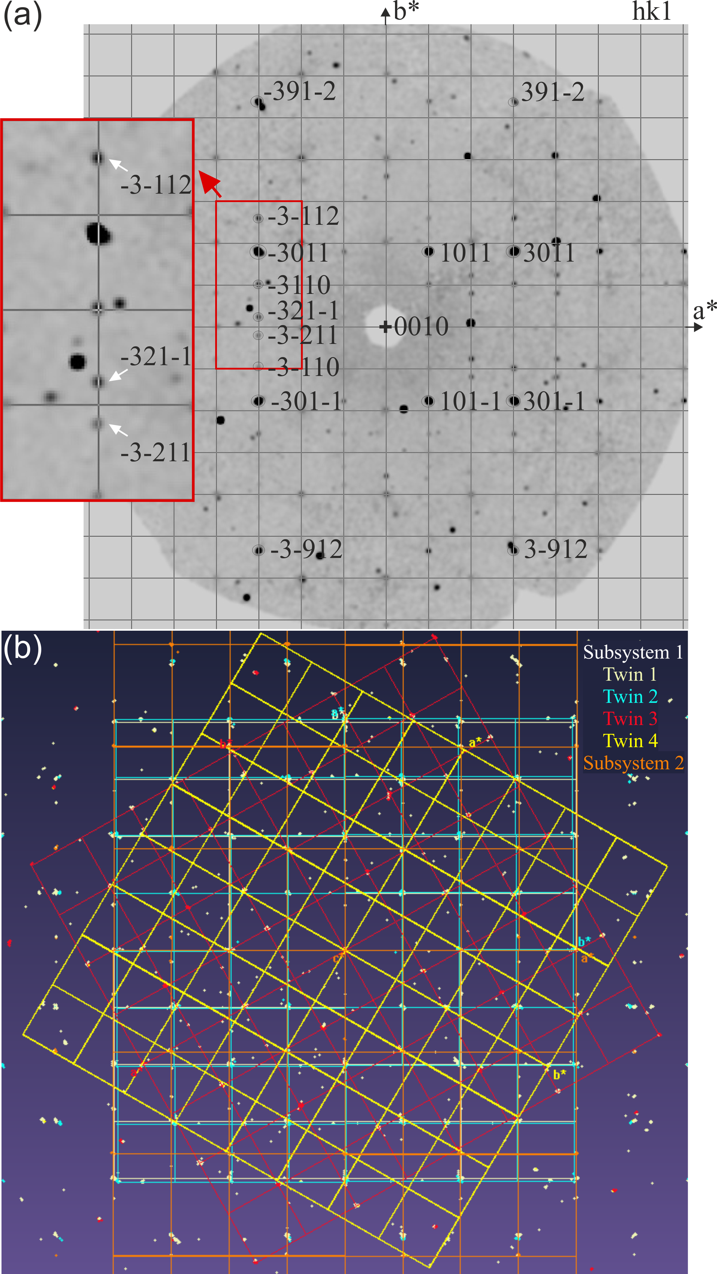
(PbS)1.18VS2 crystals were grown using chemical vapor transport according to a modified recipe of Gotoh et al. [23, 24]. They crystallize as a layer composite structure (see Figs. LABEL:fgr:fig_s1 – LABEL:fgr:fig_s3 in the Supplemental Material [24]), where subsystems 1 and 2 are PbS and VS2, respectively. Subsystems 1 and 2 have parallel sublattice parameters a and c, while b is the incommensurate axis. Using the superspace formalism, indices , , , and [21] are necessary to index both reciprocal sublattices of (PbS)1.18VS2, where is the modulation vector of sublattice 2, and is the modulation vector of sublattice 1.
A diffraction vector Q is given by , where are the reflection indices containing information from both subsystems;
-
•
, main reflections common for both subsystems;
-
•
, main reflections for the first subsystem, order satellites for the second subsystem;
-
•
, , main reflection for the second subsystem, order satellites;
-
•
, , pure satellite reflection of order and order for the first and second subsystem, respectively.
In a previous attempt to elucidate the crystal structure of (PbS)1.18VS2, Gotoh et al. [23, 25] observed satellites on electron diffraction photographs, but not by single crystal XRD. Hence, the structure was analyzed using the superspace formalism without observed satellites.
In our case, not only satellites were observed by single crystal X-ray diffraction, but also twins were present in the data, as shown in the reconstructed reciprocal space section (Fig. 1). Using a monoclinic unit cell to index both subsystems, the and parameters are common to both subsystems: subsystem 1 (PbS) has unit cell parameters , , Å, and . Subsystem 2 (VS2) has Å. Figure 1(a) contains reflections belonging to subsystems 1 and 2, weak satellites, and several reflections that are not indexed. The extra reflections can be indexed, if other twins are included during the data integration. Since the two subsystems have either a distorted cubic or a hexagonal subcell, there are several possible configurations of layer organization, which allows for a range of twin orientations. Figure 1(b) shows the reciprocal space map containing four possible twins from the PbS subsystem: twin 1 has 30.8 of indexation, twin 2 has 26.6 of indexation, twin 3 has 24.5 of indexed peaks, and twin 4 has 4.8 of indexed peaks. The second subsystem is shown in orange and has 19.7 of indexed peaks. Each twin has part of the indexed peaks overlapped with other components. Data integrated for the structure analysis [26] includes three twins, which can be seen in Fig. LABEL:fgr:fig_s3(a) in the Supplemental Material [24]. The first twin is the one with the highest percentage of indexed reflections and has the main reflections from subsystems 1 and 2, plus satellites (Fig. LABEL:fgr:fig_s3(b) in the Supplemental Material [24]). Even though the relation between twins 2, 3, and 4 to twin 1 seems to be a rotation of approximately 180, 30, and 60 around , respectively (see Fig. 1(b)), the real rotation is along all the three axes , , and .
From a crystallographic point of view, a variety of twin angles can be expected, but the dominant twist angles here, have a preference angle of approximately 0 and 180 with respect to the twin with the highest indexation. Table. LABEL:tab:tab_s1 in the Supplemental Material [24] shows this effect in more detail. This is probably no coincidence, as the difference between the twist angle of two twins being approximately 0 twins would result in an 3R-type alignment and 60 or 180 twins would result in an 2H-type alignment [13] of the VS2-layer, respectively. This indicates that these two configurations are local energy minima, similar as has been observed in exfoliated van der Waals heterostructures [13].
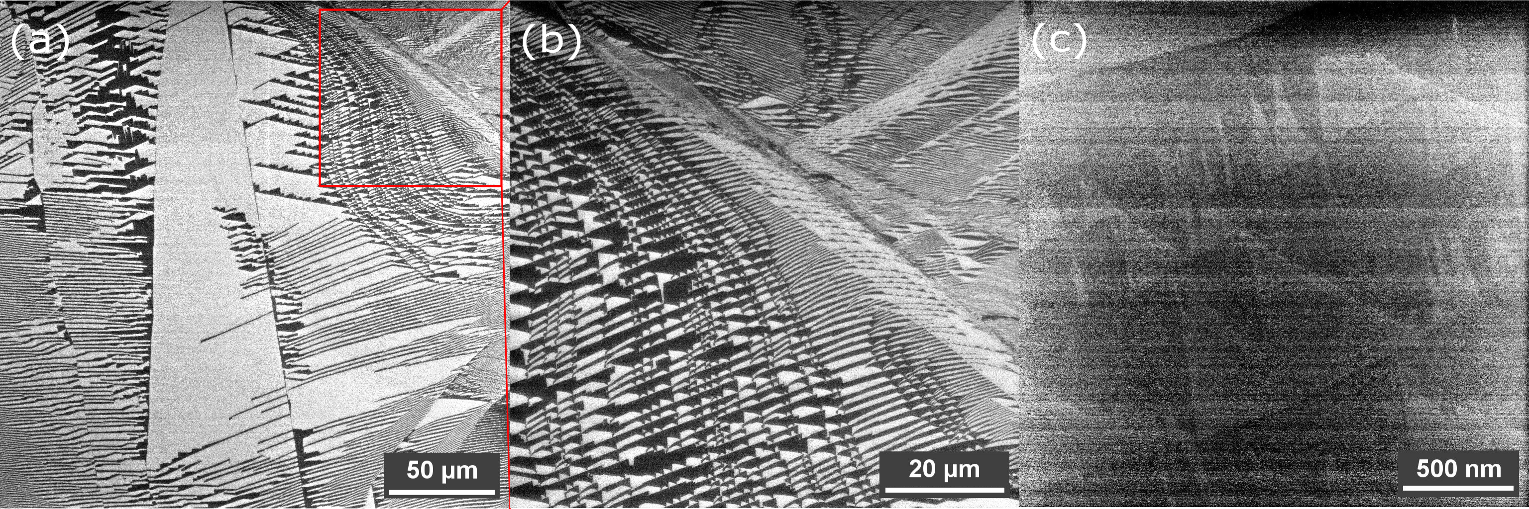
To investigate the possible presence of sliding ferroelectricity between the different twins, secondary electrons imaging (SE) in a SEM was used to map the surface electrical potential and spatial variations of topography [27, 28, 29]. In Fig. 2, SE images of the (PbS)1.18VS2 surface cleaved in ambient conditions are shown. Clearly visible is the presence of a complex domain structure, where the shape of the domains is either preferentially aligned stripes or triangular-like. Similar domain shapes were observed before in exfoliated TMD-based van der Waals heterostructures, which were stacked on top of each other with a small twist angle between the layers. Those domains were shown to be ferroelectric [5, 6, 7, 8]. The triangular domain indicates that the layers in those areas have a 3R-type alignment, and the triangular moiré is induced by the distorted hexagonal VS2 layer. SE imaging of a 2H-type alignment is shown in Fig. LABEL:fgr:fig_s6 in the Supplemental Material [24].
The period of the domain network is for very small twist angles equal to , where is the lateral lattice constant of VS2 [7]. The largest observed triangular shape domains with lateral dimensions around 30 m suggest that the smallest twist angles present between the hexagonal lattices of the VS2 layers are of the order 10-4 rad.
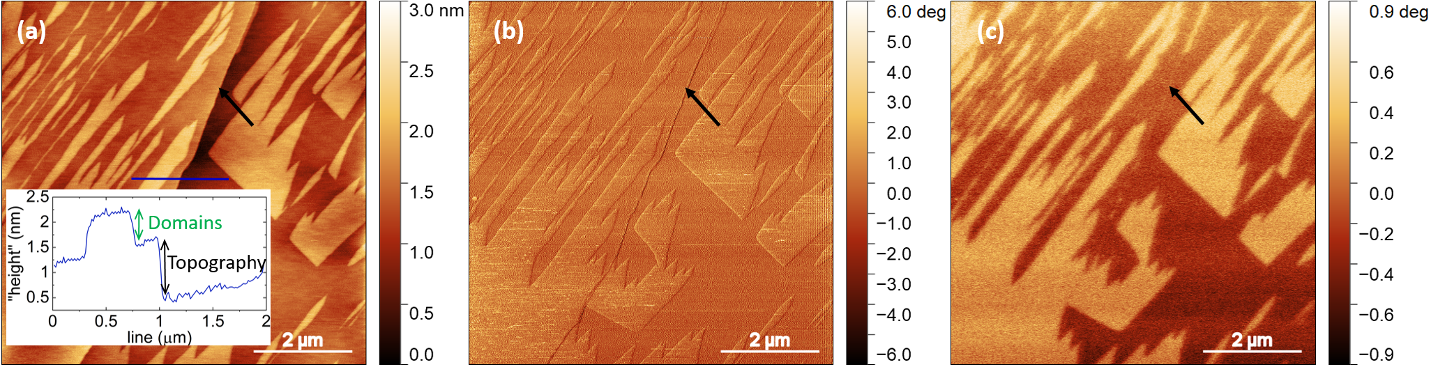
As recently shown, the ferroelectric domains in van der Waals moiré materials can be straightforwardly imaged using electric force microscopy (EFM) [9, 30]. Even in standard tapping mode atomic force microscopy (TM-AFM), the phase and even topography can be used for imaging moiré interlayer modulation of the van der Waals potential [31]. Our TM-AFM and EFM measurements were performed on freshly cleaved single crystals. Like the SEM images presented in Fig. 2, domain structures with similar shapes and sizes were found, depending on the position at the sample surface. In Fig. 3, the topography and phase of the TM-AFM and EFM’s phase are shown. When Fig. 3(a) and (b) are compared, two different features can be seen in both the topography and TM-AFM phase contrast; the terrace step going through the whole image, marked by the arrow, and the domains. In the topography image, the features appear as approximately 1 nm high steps. In the TM-AFM phase image, the domains induce a constant phase shift, resulting from different energy dissipation due to the modulation of van der Waals forces in the moiré structures [31] while the terraces are visible only as lines along the step edges.
The domains are also visible in the EFM phase image in Fig. 3(c) (lift height 15 nm, zero bias voltage). The domains show a large contrast, while the terrace edge is barely visible. When a bias voltage is applied, the phase difference between both domains becomes larger, and the contrast can be switched when an opposite bias voltage is applied (not shown). This effect is similar to measurements on der Waals heterostructures [31, 7, 6, 9]. However, in our case, the domains are much more pronounced in the topography than reported. This is probably due to the samples’ bulk character and surface quality.
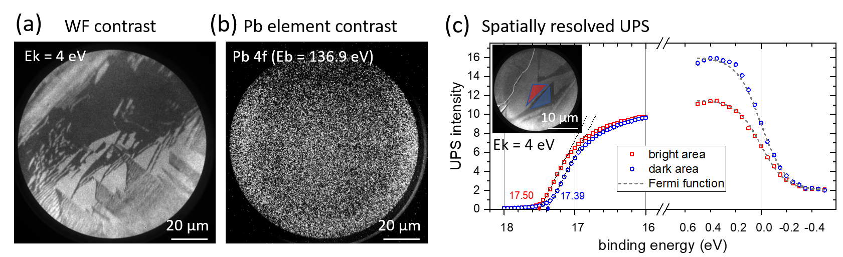
Energy-filtered PEEM imaging can provide spatial information on the elemental composition, but also on changes in the work function caused by the different alignment of the electric polarization, as already shown in the early 1970s by Le Bihan [32, 33] and Morlon et al. [34] for ferroelectric domains in BaTiO3.
In Fig. 4(a), an energy-filtered PEEM image is shown acquired using a Hg lamp and an analyzer kinetic energy setting of 4 eV. In this mode, the image is dominated by secondary electrons and reflects differences in the work function. The work function contrast reveals a domain structure similar to what was also observed using SEM and SPM. To verify if these domains are not caused by alternations of either a PbS or VS2 termination of the crystal, an elemental map of the same area was measured using energy-filtered PEEM of the Pb 4f core spectrum (see Fig. LABEL:fgr:fig_s4 in the Supplemental Material [24] for the complete XPS spectrum). As the intensity of the PEEM imaging is very sensitive to the stacking of the final layers of the crystal, a different termination of the sample should result in the appearance of PbS and VS2 domains. As shown in Fig. 4(b), no contrast is visible, so it can be concluded that the termination of the whole area is the same.
Subsequently, spatially resolved ultraviolet photoelectron spectroscopy (UPS) was used to measure the work function of both domains. In Fig. 4(c), the UPS spectra of the two polarized regions are shown for low binding energies, [-0.5 - +0.5 eV], and high binding energies, [16 - 18 eV]. The low energy window reflects the density of states at the valence band maximum, whereas the high energy window reflects the drop in intensity due to the cut-off energy of secondary electrons. Comparing the data of both domains, it is visible that the Fermi edge remains at the same position. The fit by a Fermi function, dashed lines in Fig. 4(c), gives a Fermi energy position eV. In contrast, the secondary electron energy cut-off around 17.5 eV, derived from the tangential fit, is downshifted by 0.11 eV between the two domains. This indicates that the change in the UPS spectra is due to a different work function of both domains.
In the following part, we discuss the consequences of the observed twins and domains in the (PbS)1.18VS2 crystals. In contrast to ‘traditional’ electrically isolating ferroelectrics, (PbS)1.18VS2 crystals are semiconducting [19], according to electric transport measurements, or even metallic, according to UPS or UV-VIS absorption spectroscopy [35]. The comparably large conductivity makes the ‘traditional’ electrical characterization used to identify ferroelectric materials and to switch the ferroelectric domains very challenging. Nevertheless, here we show using the combination of the structural data obtained with single crystal XRD and the observed domains obtained using various technique that sliding ferroelectricity is present in bulk MLC crystals .
Generally, the crystal structure refinement of MLCs using single crystal XRD is challenging [36]. However, moiré patterns in van der Waals heterostructures, which work as a magnifying glass [37], provide essential information for the structural refinement of the very small twist angle and strain variations between the different layers.
The presence of moiré structures in (PbS)1.18VS2 make this class of materials a possible next platform to explore the physics of strong electronic correlations and possible non-trivial band topology. A first hint of such strongly correlated physics can be found in low-temperature studies which were performed in the past on the MLC LaS1.17VS2, which can be either electron or hole-doped using Pb and Sr [38, 39].
To conclude, sliding ferroelectricity has been observed in bulk (PbS)1.18VS2 crystals. The mutual interaction between the PbS and VS2 subsystems is the key mechanism, which introduces well-defined groups of twins in the (PbS)1.18VS2 bulk crystal, where the stacking of the twins determines if there is locally a 2H- or 3R-type alignment. The possibility to steer interaction-driven twist angles in bottom-up growth can provide a new pathway to create large-scale moiré landscapes, twintronics, both in thin films and bulk crystals and might remove the problems with manual stacked devices [15].
We thank Peter Minárik for the FIB lamella preparation and Jan Michalička for the support during the HRTEM measurement. The authors acknowledge the support provided by the Czech Science Foundation (project No. 22-04816S) and from the Czech Ministry of Education, Youth, and Sports (MEYS) project SOLID21 (Project No. CZ.02.1.01/0.0/0.0/16-019/0000760). Single-crystal growth and characterization were performed in MGML, within the program of Czech Research Infrastructures (project no. LM2023065). CzechNanoLab (project no. LM2023051) funded by MEYS CR is acknowledged for the financial support of the TEM measurements at CEITEC Nano Research Infrastructure.
References
- Li and Wu [2017] L. Li and M. Wu, ACS Nano 11, 6382 (2017).
- Yang et al. [2018] Q. Yang, M. Wu, and J. Li, J. Phys. Chem. Lett. 9, 7160 (2018).
- Yang and Wu [2023] L. Yang and M. Wu, Adv. Funct. Mater. n/a, 2301105 (2023).
- Atri et al. [2023] S. S. Atri, W. Cao, B. Alon, N. Roy, M. V. Stern, V. Falko, M. Goldstein, L. Kronik, M. Urbakh, O. Hod, and M. B. Shalom, (2023), arXiv:2305.10890 [cond-mat.mtrl-sci] .
- Stern et al. [2021] M. V. Stern, Y. Waschitz, W. Cao, I. Nevo, K. Watanabe, T. Taniguchi, E. Sela, M. Urbakh, O. Hod, and M. B. Shalom, Science 372, 1462 (2021).
- Yasuda et al. [2021] K. Yasuda, X. Wang, K. Watanabe, T. Taniguchi, and P. Jarillo-Herrero, Science 372, 1458 (2021).
- Weston et al. [2022] A. Weston, E. Castanon, V. Enaldiev, F. Ferreira, S. Bhattacharjee, S. Xu, H. Corte-León, Z. Wu, N. Clark, A. Summerfield, T. Hashimoto, Y. Gao, W. Wang, M. Hamer, H. Read, L. Fumagalli, A. Kretinin, S. Haigh, O. Kazakova, A. Geim, V. Fal’ko, and R. Gorbachev, Nat. Nanotechnol. 17, 390 (2022).
- Rogée et al. [2022] L. Rogée, L. Wang, Y. Zhang, S. Cai, P. Wang, M. Chhowalla, W. Ji, and S. P. Lau, Science 376, 973 (2022).
- Woods et al. [2021] C. R. Woods, P. Ares, H. Nevison-Andrews, M. J. Holwill, R. Fabregas, F. Guinea, A. K. Geim, K. S. Novoselov, N. R. Walet, and L. Fumagalli, Nat. Comm. 12, 347 (2021).
- Garcia-Ruiz et al. [2023] A. Garcia-Ruiz, V. Enaldiev, A. McEllistrim, and V. I. Fal’ko, (2023), arXiv:2305.10896 [cond-mat.mtrl-sci] .
- Carr et al. [2018] S. Carr, D. Massatt, S. B. Torrisi, P. Cazeaux, M. Luskin, and E. Kaxiras, Phys. Rev. B 98, 224102 (2018).
- Gargiulo and Yazyev [2017] F. Gargiulo and O. V. Yazyev, 2D Mater. 5, 015019 (2017).
- Rosenberger et al. [2020] M. Rosenberger, H. Chuang, M. Phillips, V. Oleshko, K. McCreary, S. Sivaram, C. Hellberg, and B. Jonker, ACS Nano 14, 4550 (2020).
- Weston et al. [2020] A. Weston, Y. Zou, V. Enaldiev, A. Summerfield, N. Clark, V. Zólyomi, A. Graham, C. Yelgel, S. Magorrian, M. Zhou, J. Zultak, D. Hopkinson, A. Barinov, T. Bointon, A. Kretinin, N. Wilson, P. Beton, V. Fal’ko, S. Haigh, and R. Gorbachev, Nat. Nanotechnol. 15, 592 (2020).
- Lau et al. [2022] C. Lau, M. Bockrath, K. F. Mak, and F. Zhang, Nature 602, 41 (2022).
- Miao et al. [2022] L. Miao, N. Ding, N. Wang, C. Shi, H.-Y. Ye, L. Li, Y. Yao, S. Dong, and Y. Zhang, Nat. Mater. 21, 1158 (2022).
- Suzuki et al. [2014] R. Suzuki, M. Sakano, Y. Zhang, R. Akashi, D. Morikawa, A. Harasawa, K. Yaji, K. Kuroda, K. Miyamoto, T. Okuda, K. Ishizaka, R. Arita, and Y. Iwasa, Nat. Nanotechnol. 9, 611 (2014).
- Mortelmans et al. [2021] W. Mortelmans, S. De Gendt, M. Heyns, and C. Merckling, Appl. Mater. Today 22, 100975 (2021).
- Wiegers [1996] G. Wiegers, Prog. Solid. State Ch. 24, 1 (1996).
- Petříček et al. [1991] V. Petříček, K. Malý, P. Coppens, X. Bu, I. Císařová, and A. Frost-Jensen, Acta Crystallogr. Sect. A 47, 210 (1991).
- Císařová et al. [1993] I. Císařová, K. Malý, V. Petříček, and P. Coppens, Acta Crystallogr. Sect. A 49, 336 (1993).
- Oxford UK [2022] R. C. Oxford UK, “Rigaku Oxford Diffraction, CrysAlisPro Software system,” (2022).
- Gotoh et al. [1990] Y. Gotoh, M. Goto, K. Kawaguchi, Y. Oosawa, and M. Onoda, Mater. Res. Bull. 25, 307 (1990).
- sup [2023] “See supplemental material at xxx for experimental details, XPS core level spectroscopy, TEM and the reciprocal space map of (PbS)1.18VS2 , which includes refs. [40-55].” (2023).
- Mitsuko et al. [1990] O. Mitsuko, K. Katsuo, G. Yoshito, and O. Yoshinao, Acta Crystallogr. Sect. B 46, 487 (1990).
- cry [2023] “A detailed description of the crystal structure is under preparation and will be published elsewhere.” (2023).
- Andersen et al. [2021] T. I. Andersen, G. Scuri, A. Sushko, K. De Greve, J. Sung, Y. Zhou, D. S. Wild, R. J. Gelly, H. Heo, D. Bérubé, A. Y. Joe, L. A. Jauregui, K. Watanabe, T. Taniguchi, P. Kim, H. Park, and M. D. Lukin, Nat. Mat. 20, 480 (2021).
- Bihan and Maussion [1972] R. L. Bihan and M. Maussion, J. Phys. Colloques 33, C2 (1972).
- Hunnestad et al. [2020] K. Hunnestad, E. Roede, A. van Helvoort, and D. Meier, J. Appl. Phys. 128, 191102 (2020).
- Moore et al. [2021] S. L. Moore, C. Ciccarino, D. Halbertal, L. McGilly, N. Finney, K. Yao, Y. Shao, G. Ni, A. Sternbach, E. Telford, B. Kim, S. Rossi, K. Watanabe, T. Taniguchi, A. Pasupathy, C. Dean, J. Hone, P. Schuck, P. Narang, and D. Basov, Nat. Commun. 12, 5741 (2021).
- Chiodini et al. [2022] S. Chiodini, J. Kerfoot, G. Venturi, S. Mignuzzi, E. Alexeev, B. T. Rosa, S. Tongay, T. Taniguchi, K. Watanabe, A. Ferrari, and A. Ambrosio, ACS Nano 16, 7589 (2022).
- Bihan [1970] R. L. Bihan, C. R. Acad. Sci. Ser. B 270, 741 (1970).
- Bihan [1972] R. L. Bihan, C. R. Acad. Sci. Ser. B 275, 29 (1972).
- Morlon et al. [1970] B. Morlon, E. Coquet, and A. Devin, C. R. Acad. Sci. Ser. B 270, 283 (1970).
- Sourisseau et al. [1995] C. Sourisseau, R. Cavagnat, M. Fouassier, J. L. Tirado, and J. Morales, J. Raman Spectrosc. 26, 675 (1995).
- Ng and McQueen [2022] N. Ng and T. McQueen, APL Mater. 10, 100901 (2022).
- Cosma et al. [2014] D. A. Cosma, J. Wallbank, V. Cheianov, and V. Fal’ko, Faraday Discuss. 173, 137 (2014).
- Ino et al. [2004] A. Ino, T. Okane, S.-I. Fujimori, A. Fujimori, T. Mizokawa, Y. Yasui, T. Nishikawa, and M. Sato, Phys. Rev. B 69, 195116 (2004).
- Yasui et al. [1995] Y. Yasui, T. Nishikawa, Y. Kobayashi, M. Sato, T. Nishioka, and M. Kontani, J. Phys. Soc. Jpn. 64, 3890 (1995).
- Bruker Nano GmbH [20xx] G. Bruker Nano GmbH, Berlin, “Software: Esprit family,” (20xx).
- Petříček et al. [2014] V. Petříček, M. Dušek, and L. Palatinus, Z. Kristallogr. Cryst. Mater. 229, 345–352 (2014).
- Palatinus and Chapuis [2007] L. Palatinus and G. Chapuis, J. Appl. Crystallogr. 40, 786 (2007).
- Momma and Izumi [2011] K. Momma and F. Izumi, J. of Appl. Crystallogr. 44, 1272 (2011).
- Ettema and Haas [1993] A. R. H. F. Ettema and C. Haas, J. Condens. Matter Phys. 5, 3817 (1993).
- Brandt [2003] J. Brandt, Geometric and electronic structure of misfit layered compounds and epitaxial thin films of PbS on transition metal dichalcogenides, Ph.D. thesis, Mathematisch-Naturwissenschaftlichen Fakultát, Christian-Albrechts-Universität, Kiel (2003).
- Hossain et al. [2018] M. Hossain, J. Wu, W. Wen, H. Liu, X. Wang, and L. Xie, Adv. Mater. Interfaces 5, 1800528 (2018).
- Zhang et al. [2017] Z. Zhang, J. Niu, P. Yang, Y. Gong, Q. Ji, J. Shi, Q. Fang, S. Jiang, H. Li, X. Zhou, L. Gu, X. Wu, and Y. Zhang, Adv. Mater. 29, 1702359 (2017).
- Hossain et al. [2021] M. Hossain, M. Iqbal, J. Wu, and L. Xie, RSC Adv. 11, 2624 (2021).
- Silversmit et al. [2004] G. Silversmit, D. Depla, H. Poelman, G. B. Marin, and R. De Gryse, J. Electron Spectrosc. Relat. Phenom. 135, 167 (2004).
- Göhler et al. [2022] F. Göhler, S. Ramasubramanian, S. K. Rajak, N. Rösch, A. Schütze, S. Wolff, D. L. M. Cordova, D. C. Johnson, and T. Seyller, Nanoscale 14, 10143 (2022).
- Göhler et al. [2018] F. Göhler, G. Mitchson, M. B. Alemayehu, F. Speck, M. Wanke, D. C. Johnson, and T. Seyller, Journal of Physics: Condensed Matter 30, 055001 (2018).
- Leiro et al. [1998] J. Leiro, K. Laajalehto, I. Kartio, and M. Heinonen, Surface Science 412-413, L918 (1998).
- Fong et al. [2006] D. D. Fong, A. M. Kolpak, J. A. Eastman, S. K. Streiffer, P. H. Fuoss, G. B. Stephenson, C. Thompson, D. M. Kim, K. J. Choi, C. B. Eom, I. Grinberg, and A. M. Rappe, Phys. Rev. Lett. 96, 127601 (2006).
- Baniecki et al. [2009] J. Baniecki, M. Ishii, K. Kurihara, K. Yamanaka, T. Yano, K. Shinozaki, T. Imada, and Y. Kobayashi, J. Appl. Phys. 106, 054109 (2009).
- Krug et al. [2010] I. Krug, N. Barrett, A. Petraru, A. Locatelli, T. Mentes, M. Niño., K. Rahmanizadeh, G. Bihlmayer, and C. Schneider, Appl. Phys. Lett. 97, 222903 (2010).