Silicon photonic devices for scalable quantum information applications
Abstract
With high integration density and excellent optical properties, silicon photonics is becoming a promising platform for complete integration and large-scale optical quantum information processing. Scalable quantum information applications need photon generation and detection to be integrated on the same chip, and we have seen that various devices on the silicon photonic chip have been developed for this goal. This paper reviews the relevant research results and state-of-the-art technologies on the silicon photonic chip for scalable quantum applications. Despite the shortcomings, properties of some components have already met the requirements for further expansion. Furthermore, we point out the challenges ahead and further research directions for on-chip scalable quantum information applications.
pacs:
I. INTRODUCTION
Quantum information science is a new frontier subject combining quantum mechanics and information science. The quantum nature of particle superposition, entanglement, and measurement are applicable for more efficient information processing, computation, transmission and storage. The development of quantum information industry promises more powerful computing power, high security information communication and a deeper understanding of nature. It is expected to resolve numerous scientific problems that are difficult to be effectively solved by existing classical techniques. For example, absolutely secure information transmission Bennett1984 ; Gisin2002 , exponentially or polynomial accelerating the resolving of hard scientific problems Shor1994 ; Grover1997 , efficient simulation of molecular structures Feynman1982 and precision measurement beyond the standard quantum limit Giovannetti2011 .
In the last decades, quantum fundamental science is rapidly transformed into quantum technologies with huge resources invested by global academia, research centers and industry. Quantum scientific research is moving from the stage of principle verification of quantum rules to the stage of practical device research and development governed by these rules. We have seen that quantum computational advantage realized in different systems Arute2019 ; Zhong2020 ; Wu2021 , quantum key distribution via thousands of kilometer level satellite-to-ground quantum network Liao2017 and quantum-enhanced sensing for gravitational waves Abbott2016 , magnetic field Boss2017 and mass of nanoparticle Zheng2020 .
Photon, as one ideal information carrier, has been widely used in quantum information processing and shows several unique advantages such as fast transmission speed, low noise, multiple degrees of freedom for information encoding and high capacity. Besides, light has a wide range of applications in energy, communication, computation, medical care etc. These increasingly mature industrial applications provide favorable supports for photonic quantum technologies. Currently, fibre optical communication technology has become the pillar for information transmission, and photonic integration and optoelectronic integration for information processing has developed rapidly in recent years for the future all-optical network. Therefore, optical quantum systems are becoming a promising platform for quantum information processing O'brien2009 ; Flamini2018 ; Slussarenko2019 .
To enhance the complexity of quantum optical experiments, optical quantum systems tend to use photonic integrated circuits Wang2020 . Compared to systems that use discrete optical components on an optical table, the integrated photonic devices enable localize and manipulate photons at micro/nano scales, and thus greatly improve the stability and scalability of quantum optical experiments and provide a complex and compact quantum photonics approach for quantum communication, sensing and computing applications Lu2021 . Therefore, the integrated techniques will lead quantum applications moving out of the laboratory and into large-scale and practical. Multiple optical waveguide materials, such as silica Politi2008 ; Jiang2017 ; Zhang20192 ; Li2022 , silicon (Si) Silverstone2016 , silicon nitride (SiN) Zhang2018 ; Lu2019 ; Taballione2021 ; Ren2022 , lithium niobate Jin2014 ; Wang20172 ; Xu2022 , and techniques, such as lithography Bojko2011 , laser-writing Sugioka2014 , have been developed. Among those materials, silicon photonics is a good candidate because of its easy preparation, high integration density and excellent optical properties Rudolph2017 . Also thanks to the leadership of classical silicon photonics in large-scale photonic integrated circuits, the performance of silicon-based devices has been rapidly improved Thomson2016 .
Currently, photonic devices on the silicon chip for various quantum applications have been developed, sucn as high-efficiency chip-fiber coupler Son2018 , large-scale programmable quantum photonic circuits Harris2016 and single-photon detectors Pernice2012 . However, scalable quantum applications put forward new and higher requirements for integrated photonic devices. For example, high isolation on-chip filter is needed to separate pump and single-photon level signals, and modulator should also operate at cryogenic condition. In this paper, we review the relevant research results and state-of-the-art technologies on the silicon photonic chip for scalable quantum applications. Since silicon optical chips can be easy prepared, their applications are very wide and diverse. Here we just review common complementary metal oxide semiconductor (CMOS) compatible silicon-on-insulator (SOI) chips with telecom optical band O + C. We’re glad to see that properties of some integrated components have already met the requirements for further quantum application and expansion. Furthermore, we point out the challenges ahead and further research directions. This review mainly focus on advances of silicon photonic devices, and for more information about related novel quantum experiments, we recommend some related good reviews, such as preparation of photon-pair sources with silicon photonics Feng2020 ; Chen2021 , advances of quantum experiments on the silicon chip Wang2020 ; Adcock2020 , and hybrid integrated techniques for quantum applications Elshaari2020 ; Kim2020 .
The review is structured as follows: Section II reviews the state-of-the-art technologies of basic components on the silicon chip, such as on-chip photon sources, detectors, chip interconnects and so on. In Section III, we introduce some key and fundamental quantum information processing in silicon photonic circuits and review research works on multiphoton and high dimensional applications, quantum error correction, quantum key distribution as well as quantum state teleportation between chips. These excellent works leads to scalable quantum computing and communication. Finally, in Section IV, we outlook the future of silicon photonics for scalable quantum information applications and provide challenges for further scaling.
II. Scalable techniques on silicon photonic chips
Scalable quantum information processing needs to improve the complexity on the single chip as much as possible. Different degrees of freedom of photons should achieve universal quantum operation, and quantum photonic source, detector, logic operation and other core functions should be improved to high quality and be integrated on the same chip. Considering the limited chip size and difficulty in hybrid integration with different materials, multifunction chip can also be achieved by high efficiency optical interconnection for quantum communication and distributed quantum computing and metrology. Accordingly, we divide the state-of-the-art techniques in silicon photonics into two aspects to review, single-chip and interconnection technologies. The contents of this section include single-photon sources, photon detection, wavelength and mode division multiplexing and cryogenic techniques on the single chip and chip interconnects techniques.
.1 A. Single-photon sources
| Ref. | Structure | Bandwidth | PGR/SER | CAR | Wavelength | |
| Li2017 | Single-mode waveguide | 100 GHz | 0.7 MHz.mW-2 | 80 | – – | 1538.2 & 1562.2 nm |
| Ma2017 | Micro-ring resonator | 2.1 GHz | 149 MHz.mW-2 | 12105 | 0.00533 | 1535.5 & 1574.7 nm |
| Paesani2020 | Multimode waveguide | 4 nm | 18.6 MHz.mW-2 | – – | 0.053 | 1516 & 1588 nm |
| Zhou2018 | GaN Defect | 3–50 nm | 1.5 MHz | – – | 0.05 | 1085–1340 nm |
| Zhao2021 | 2D MoTe2 | 8.5–37 nm | – – | – – | 0.058 | 1080–1550 nm |
| Hollenbach2020 | G center | 0.5 nm | 99 kHz | – – | 0.07 | 1278 nm |
| Higginbottom2022 | T center | 255 MHz | – – | – – | 0.2 | 1326 nm |
Scalable quantum photonic information processing requires multiple high-quality single photon sources. Today, there are two promising approaches to achieving a near-deterministic single photon source, one is based on multiplexing an array of probabilistic parametric photon pair sources, and the other is based on solid-state single-photon emitters.
With strong third-order nonlinear response, silicon waveguides can be directly used to prepare photon pair sources via spontaneous four-wave mixing process (SFWM) Li2017 . Many techniques were developed to improve photonic source quality, such as using micro-ring resonators Ma2017 ; Liu2020 ; Burridge2020 and introducing special phase-matching condition Paesani2020 . More details are given in Table I. Upon pair generation, one of the photons is detected to herald the presence of its partner. Although each photon pair source is probabilistic, multiple heralded single photons can be dynamically switched to one single output mode, and thus increasing the output probability. Any degree of freedom of the photon pairs can be used for multiplexing, such as path, frequency and time bins. Also, these can be combined to multiplicatively increase the number of multiplexed modes. In ref. Collins2013 , a 63.1% efficiency increase in the heralded single-photon output has been demonstrated through multiplexing photons generated in two silicon waveguides. In ref. Zhang2015 , the enhancement was increased to 905% by using a silicon waveguide pumped by time and wavelength division multiplexed pulses. In ref. Xiong2016 , 100% enhancement was achieved by multiplexing photons from four temporal modes. Recently, although not within silicon photonics, a factor of 9.7 enhancement in efficiency has been realized using optical delay to multiplex 40 heralded single-photon sources Kaneda2019 .
Despite these developments, on-chip integration of multiplexing systems is still an outstanding challenge, and the main obstacle is the device loss. For example, assuming that 1 ns delay line corresponds to 10 cm long silicon waveguide, and the waveguide has the state-of-the-art low loss of 0.08 dB/m Lee2012 , 100 ns delay line will introduce 0.8 dB loss, which is still much higher than that in commercial fiber. The integrated high-speed switch, one necessary component in multiplexing systems, usually needs ion doping or hybrid integration with other electro-optic materials such as lithium niobate He2019 , and these post-processing processes always introduce extra losses. Significant reduction in these losses will enable multiple near-deterministic single photon sources achieved on the silicon chip with probabilistic nonlinear parametric processes.
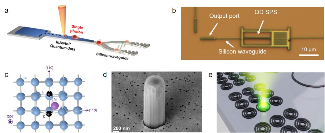
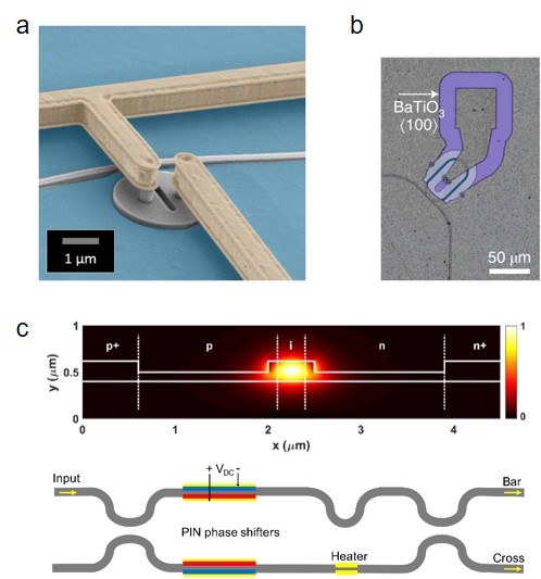
Another approach, the solid-state emitters generate deterministic single photons and can be integrated or transferred on the silicon photonic circuits. Since silicon is opaque below around 1100 nm, single-photon emitters integrated with silicon would need to radiate photons beyond this wavelength limit. Multiple quantum dots at telecommunication wavelengths have been demonstrated Haffouz2018 ; Kim2017 ; Muller2018 ; Katsumi2018 ; Katsumi2019 ; Zhou2018 ; Redjem2020 ; Zhao2021 . Among them, the most common are semiconductor quantum dots including InAsP Haffouz2018 , InAs/InP Kim2017 ; Muller2018 and InAs/GaAs Katsumi2018 ; Katsumi2019 , etc. By using emission-wavelength-optimized waveguides, ref. Haffouz2018 demonstrated photon emission from single InAsP quantum dot with large tuning range from 880 to 1550 nm. With hybrid integration techniques, transfer semiconductor quantum dots on the silicon waveguides (Fig. 1a and 1b) has been implemented with values around 0.3 Kim2017 ; Katsumi2018 ; Katsumi2019 . By using localized defects in the gallium nitride crystal, high-quality solid-state quantum emitters in the telecom range has been achieved Zhou2018 . Even at room temperatures, was obtained with continuous wave (CW) laser excitation. Two-dimensional (2D) materials show many amazing properties and have also been used to produce quantum emitters, for example, telecom-wavelength single-photon emitters via coupling 2D molybdenum ditelluride (MoTe2) to nano-pillar arrays have been reported with and under pulsed and CW laser excitation, respectively Zhao2021 . Colour centers, known as G centers and T centers, which originate from carbon-related defect in silicon, are becoming another kind of candidates with telecom-O band radiation Redjem2020 ; Hollenbach2020 ; Bergeron2020 ; Higginbottom2022 . Different from other methods, colour centers can be directly integrated into silicon waveguides without hybrid integration for large-scale quantum photonic information applications Hollenbach2021 ; Prabhu2022 . For example, tens of thousands of individually addressed photon-spin qubits have been demonstrated with T centers, which will provide photonic links between spin qubits and greatly advance quantum information networks Higginbottom2022 .
To integrate solid-state emitters with photonic waveguides, many approaches are proposed such as nanoscale positioning approaches Liu20212 . For the important coupling efficiency, ref. Katsumi2018 showed total single-photon coupling efficiency of 63% experimentally and in theory higher than 99%. In ref. Prabhu2022 , emitters were directly integrated in silicon waveguides and showed 40% coupling efficiency in simulation. In addition, the use of optical micro-cavities deserves further consideration to improve the extraction efficiency Peng2017 ; Liu20213 ; Wei2022 . To further scaling up, simultaneous operation of multiple emitters is necessary. However, no two solid-state quantum emitters are alike when being produced experimentally. To keep coherence among them, wavelength tunability is necessary. Electronic integration or induced strain have been utilised to tune the wavelength and quantum interference between photons generated from independent quantum emitters have been demonstrated Patel2010 ; Flagg2010 . In nanophotonic devices, the wavelength tuning of the selected integrated quantum emitter have been realized Elshaari2018 ; Machielse2019 ; Katsumi2020 . The rapid development of processing and tuning techniques has enhanced the indistinguishability of photons between different emitters and increased the number of emitters on-chip. Though not in the telecom band, quantum interference of photons from two remote quantum dots with a visibility of 93.0% Zhai2022 and large-scale integration of artificial atoms in hybrid AlN photonic circuits Wan2020 have been demonstrated recently.
.2 B. Photon Detection
| Ref. | Detection Efficiency | Jitter | Dark Count Rate | Reset Time | Temperature | Number Resolving |
| Pernice2012 | 91% | 18 ps | 50 Hz | 505 ps | 1.7 K | – – |
| Akhlaghi2015 | 100% | 55 ps | 0.1 Hz | 7 ns | 2.05 K | – – |
| Vetter2016 | 30% | 32 ps | 1 Hz | 510 ps | 1.7 K | – – |
| Munzberg2018 | 70% | 480 ps | 0.1 mHz | 480 ps | 1.6 K | – – |
| Zhu2020 | 5.6% | 16.1 ps | 2 Hz | 85.8 ns | 1.0 K | 4 |
| Llin2020 | 29.4% | 134 ps | 100 kHz | – – | 125 K | – – |
| Fang2020 | 60.1% | – – | 340 kHz | 88 ns | 300 K | – – |
Photon detector converts optical signals into electrical signals and is an essential part for photonic quantum information applications. For squeezed light measurement, germanium (Ge) photodetectors integrated on silicon were developed Benedikovic2019 and homodyne detectors have been realized based on them Rafaelli2018 . Furthermore, by interfacing silicon photonics with integrated amplification electronics, complete integrated homodyne detectors have been demonstrated Tasker2021 and a shot-noise-limited bandwidth of more than 20 GHz has been achieved Bruynsteen2021 .
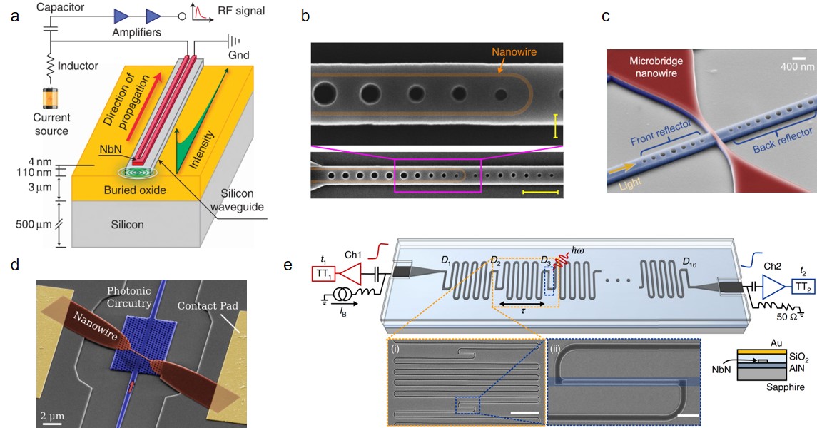
For single-photon level detection, superconducting nanowire single-photon detectors (SNSPDs) show excellent performance, such as near unity system detection efficiency Reddy2020 GHz maximum count rate Pernice2012 and picosecond level temporal resolution Korzh2020 . SNSPD uses superconducting material that works below its critical temperature. Even if only one photon hits, the energy is enough to excite the material, and generate voltage pulses subsequently. A range of superconducting materials have been developed, including NbN Pernice2012 , NbTiN Akhlaghi2015 , MoSi Li2016 and WSi Buckley2017 , etc. In vertical optical coupling between fibers and SNSPDs, fiber end faces are parallel to the SNSPDs’ photonsensitive surfaces, and photons are vertically incident to the nanowires. By optimizing the device’s vertical optical stack design, as well as the coupling of the guided fiber mode to the active detection area of the device, 98% system detection efficiency has been achieved Reddy2020 . For coupling between waveguides and SNSPDs, travelling wave coupling is used, as shown in Fig. 2a, which can achieve efficient detection of photons in the optical waveguide. This hybrid integration method directly places SNSPDs into silicon photonics, thus greatly enhancing the scalability of quantum photonic integrated circuits. For example, in ref. Pernice2012 , ballistic photon transport in silicon ring resonators has been demonstrated by exploiting high temporal resolution detectors. Besides, SNSPDs are integrated with high-quality factor microcavities to increase the coupling efficiency (Fig. 2b) Akhlaghi2015 and decrease the dark count rate (Fig. 2c and 2d) Vetter2016 ; Munzberg2018 .
Typically, single-photon detectors operate in Geiger mode, that is, the electrical signal generated by the read-out circuit indicating the detection of one photon. However, in many experiments, it is desirable to use a detector that can resolve the number of photons. By analyzing the relationship between photon numbers and resistance of the nanowire, multi-photon detection was achieved with one convertioanl SNSPD Cahall2017 . SNSPDs with photon number resolving ability has also been achieved on the AlN platform through exploring the pulse shapes of the detector output (Fig. 2e) Zhu2018 . Besides, with an integrated impedance-matching taper on the superconducting nanowire, the detector’s output amplitude turned into more sensitive to the number of photons, and detector with photon number resolving up to four, 16.1 ps timing jitter and < 2 Hz dark count rate has been demonstrated Zhu2020 .
The high-quality of SNSPDs boosts various novel applications, such as quantum computational advantage using photonsZhong2020 , imaging and spectroscopy Zhao2017 ; Wollman2019 ; Cheng2019 , and integrated quantum key distribution Beutel2021 ; Zheng2021 . Despite great progress achieved, SNSPDs cannot work without bulky and expensive cryogenic systems (< 4 K). Other types, such as germanium-on-silicon Vines2019 ; Llin2020 and InGaAs/InP single-photon detectors Zhangzhang2015 ; Fang2020 , are potential alternatives. For detection efficiency, germanium-on-silicon detectors have recently been demonstrated to be 38% at 1310 nm at 125 K Vines2019 , and InGaAs/InP detectors to be 60.1% at 1550 nm at 300 K. Further reduction of dark count rate will broaden their appeal in many quantum applications. More details about integrated single-photon detectors are summarized in Table II. In addition to these conventional devices, single-photon detection based on low-dimensional materials is emerging and has shown superior performance Wang2022 .
.3 C. Wavelength and mode division multiplexing
| Ref. | Structure | Size | Contrast | IL | FSR | Bandwidth |
| Xia2007 | High-order micro-ring | 700m2 | 40 dB | 1.8 dB | 18 nm | 310 GHz (1 dB) |
| Ong2013 | High-order micro-ring | 3000m2 | 50 dB | 3 dB | 7.3 nm | 11.6–125 GHz (3 dB) |
| Liao2014 | Unbalanced MZIs | 2 mm2 | 15 dB | 9 dB | 0.8 nm | 0.61, 0.34 and 0.21 nm (3 dB) |
| Qiu2017 | WBG | 600m2 | 35 dB | 0.6 dB | – – | 3 nm (3 dB) |
| Harris2014 | Cascaded WBG | 1280m2 | 65 dB | 3 dB | – – | 1–2 nm (3 dB) |
| Oser2020 | Cascaded WBG | 3105m2 | 60 dB | 2 dB | – – | 5.5 nm (3 dB) |
Due to the significant enhancement in demand for information processing and communication capability, much effort has been done to encode more information on one single chip. One way is to increase the integration density. Devices are developed to be more compact and their spacing to be narrower. For example, by using the concept of symmetry breaking, high-density waveguide superlattices with low crosstalk were demonstrated Song2015 .This concept has also been used to construct two-qubit quantum logic gate, and greatly reduced the footprint Zhang2021 . Recently, an ultradensely integrated multidimensional optical system with a footprint of 2030m2 has been demonstrated based on inverse-designed dielectric metasurface network Zhou2022 . Another way is to introduce new degrees of freedom through multiplexing, including wavelength division multiplexing (WDM) and mode division multiplexing (MDM).
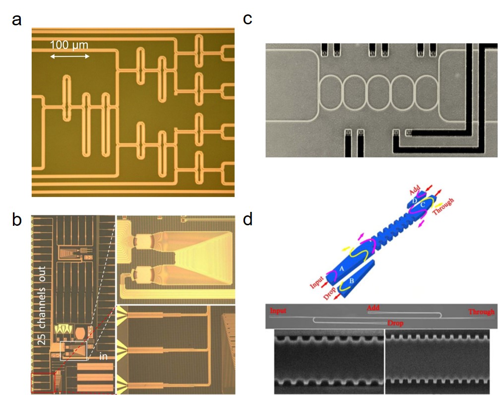
WDM is a technique that encodes information with different optical wavelengths as different channels. Structures like ring resonators, unbalanced MZIs, waveguide Bragg gratings (WBGs) and arrayed waveguide gratings (AWGs) are used in the WDM systems for the purpose of wavelength multiplexing and de-multiplexing Horst2013 ; Cheung2014 ; Tan2014 ; Chen2015 ; Munk2019 ; Liuliu2019 . Among them, 512 channel dense WDM Cheung2014 , channel spacing down to 17 GHz Munk2019 , hybrid integration with detectors (Fig. 3b) Liuliu2019 have been demonstrated. Although not with silicon photonics, high-speed quantum key distribution with WDM on integrated photonic circuits has been reported Price2018 .
In addition to increasing channel capacity, WDM technique is also used as filters for the spectrum manipulation in various optical systems Liu2021 . With unbalanced MZIs, an programmable filter has been demonstrated and showed the tunability of the filter central wavelength, bandwidth and variable passband shape Liao2014 . With high-order ring resonators, on-chip filters are becoming ultra-compact, ultra-high-contrast and show high flexibility Xia2007 ; Ong2013 ; Chen2014 ; Liu2019 . For example, 5th order ring resonator optical filters showed out-of-band rejection ratio of 40 dB, and insertion loss of only 1.8 dB within a footprint of 700m2 (Fig. 3c) Xia2007 . To increase the free spectral range (FSR), a resonator with a small radius of 0.8m was demonstrated and a record large FSR of 93 nm was achieved recently Liu2019 . WBGs are FSR free and could also be employed to build filters. The add-drop structure showed high-contrast and the filter bandwidths changed with the waveguide widths (Fig. 3d) Qiu2017 . More details about filting in silicon photonics are summarized in Table III. For scalable quantum information applications, these filters will be employed to filter out the pump light before detection or separate single photons at different wavelengths, as reported in refs. Harris2014 ; Oser2020 .
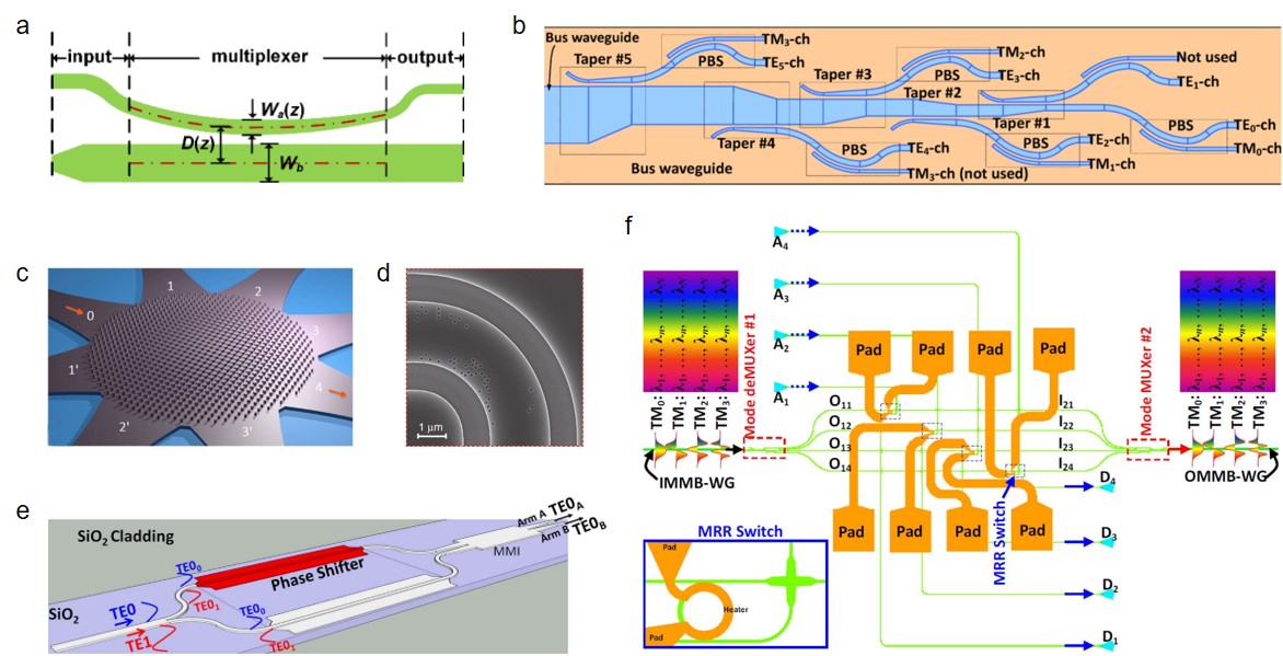
MDM is an emerging technique that uses the high-order transverse waveguide modes of multimode waveguides to encode more information Li2019 . Since multimode waveguides still support multiple wavelengths, this technique is compatible with WDM to further increase the channel capacity Luo2014 ; Dai2015 ; Wang2017 . As shown in Fig. 4, various multimode silicon photonic devices have been developed for low-loss and low-crosstalk light manipulation with multiple mode-channels in MDM systems, such as mode (de)multiplexer Dai2013 ; Guo2017 , grating couplers Lai2018 , high-speed switches Xiong2017 , sharp waveguide bends and mode-independent crossings Li2018 ; Xu2018 ; Liuy2019 . At present, mode (de)multiplexer including six mode-channels of TE polarization and four mode-channels of TM polarization has been realized Dai2018 . In addition, by using multimode optical waveguides with higher-order modes, some special silicon photonic devices that cannot be realized only with fundamental modes have been demonstrated, such as add-drop optical filters based on multimode Bragg gratings Qiu2017 ; Oser2020 .
The utilization of higher-order modes for quantum photonics has stimulated many novel applications. For example, in ref. Feng2016 , the transverse waveguide-mode degree of freedom was introduced for quantum encoding, and on-chip coherent conversion of photonic entangled quantum states between path, polarization, and transverse waveguide-mode degrees of freedom was demonstrated. In ref. Mohanty2017 , quantum interference between the guided modes was demonstrated within a multimode optical waveguide. Recently, with the help of two newly developed multimode devices, transverse mode-encoded 2-qubit logic quantum gate was realized Feng2022 , and showed the potential for universal transverse mode-encoded quantum operations and large-scale multimode multi-degrees of freedom quantum systems. The special inter-modal phase matching conditions were used to prepare quantum photonic sources. In particular, an on-chip transverse-mode entangled photon pair source via SFWM in a multimode waveguide was demonstrated Feng2019 . Furthermore, by exploiting special excitation scheme in low-loss multimode waveguides, quantum photonic source was engineered to high spectral purity and mutual indistinguishability through inter-modal SFWM Paesani2020 .
.4 D. Cryogenic techniques
The large-scale expansion of quantum photonic integrated circuits requires the integration of all functions on one single chip including quantum photonic sources, state manipulation and photon detection. Because common and efficient SNSPDs must work at cryogenic temperatures, for example, 2 K, quantum photonic sources and state manipulation processes should also extend to the same temperature condition. Besides, in quantum networks, optical interfaces with other quantum systems such as semiconductor and superconducting quantum computing systems also need to operate the whole system at cryogenic temperatures.
While passive optical components can often be used directly at low temperatures, implementation of active components and nonlinear processes has been a prominent challenge. At present, quantum state manipulation structures used in quantum photonic chips at ambient conditions are generally based on thermo-optic effect. However, the thermo-optic coefficient of silicon decreases significantly at low temperatures Komma2012 . In particular, when the temperature is several kelvin, the thermo-optic coefficient is four orders of magnitude lower than that at room temperatures, which makes thermo-optic modulators difficult to work. Another problem is that as temperatures drop, so does the cooling capacity available of the cooling system. Therefore, modulators operating at cryogenic conditions should maintain very low power consumption and heat production.
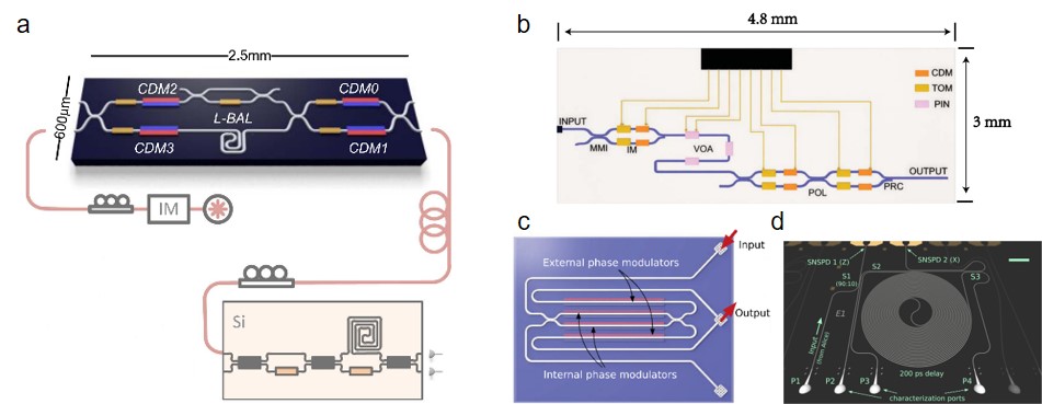
To date, some works have been reported on cryogenic modulation Gehl2017 ; Eltes2020 ; Chakraborty2020 with silicon photonics. In ref. Gehl2017 , by doping at higher concentrations, one microdisk modulator (Fig. 5a) prepared by plasma dispersion effect has been achieved at temperature 4.8 K and transmitting data rates up to 10 Gb/s has been achieved. As the first success implementation, this work opens the door for using silicon photonics to interface other systems at cryogenic conditions. Besides, electro-optic modulation at temperature 4 K by using the Pockels effect of integrated barium titanate (BaTiO3) devices has been reported (Fig. 5b)) Eltes2020 . This material showed an effective Pockels coefficient of 200 pm V-1 at 4 K, and the fabricated devices showed high electro-optic bandwidth (30 GHz), ultralow-power consumption and high-speed data modulation (20 Gb/s). Another implementation employed DC Kerr effect of the silicon waveguides and achieved phase modulation at a temperature of 5 K at GHz speeds (Fig. 5c) Chakraborty2020 . Despite these progresses, these modulation devices are still in the initial research stage, and the relevant applications in quantum information research have not been demonstrated. For large-scale quantum information applications, they should be more compact and have lower excess loss. More recently, programmable Mach–Zehnder meshes have been realized by using aluminium nitride (AlN) piezo-optomechanical actuators coupled to SiN waveguides Dong2022 , which can also operate at cryogenic conditions. Though the modulators operate in the visible band and on the SiN platform, the work demonstrates the possibility of on-chip large-scale cryogenic modulation.
In addition to cryogenic modulation, some works have also been reported on cryogenic nonlinear processes in silicon photonics Pernice2011 ; Sun2013 ; Sinclair2019 . In ref. Sinclair2019 , the temperature dependence of the two-photon absorption and optical Kerr nonlinearity of a silicon waveguide with temperatures from 5.5 to 300 K was measured, and the nonlinear figure of merit was found to be improved at cryogenic temperatures. Quantum applications, however, such as quantum photonic sources preparation by cryogenic SFWM, has not been demonstrated yet.
.5 E. Chip interconnects
Chip interconnection plays the key role in building large-scale quantum networks. In photonic quantum technologies, chip interconnection needs efficient transfer of optical signals among different optical components. However, due to the mismatch in the effective mode sizes between different components such as fibers and silicon waveguides, special coupling structures are needed Son2018 .
| Ref. | Technique | Loss | Bandwidth |
| Ding2014 | Grating coupling | 0.58 dB (TE) | 71 nm (3 dB) |
| Pu2010 | End coupling (tapered fiber) | 0.36 dB (TM); 0.66 dB (TE) | >80 nm (1 dB) |
| Fang2011 | End coupling (SMF) | 2.0 dB (TM); 1.2 dB (TE) | >120 nm (1 dB) |
| Jia2018 | End coupling (SMF) | 1.3 dB (TM); 0.95 dB (TE) | >100 nm (1 dB) |
| Luo2020 | 3D vertical coupling | 1 dB (TE and TM) | 170 nm (TE); 104 nm (TM) (1 dB) |
| Trappen2020 | 3D-printing | 1.9 dB | – – |
| Lindenmann2012 ; Lindenmann2015 ; Billah2018 | Wire bonding | 0.4 dB | – – |
| Dietrich2018 | In situ 3D nanoprinting | 0.6 dB | – – |
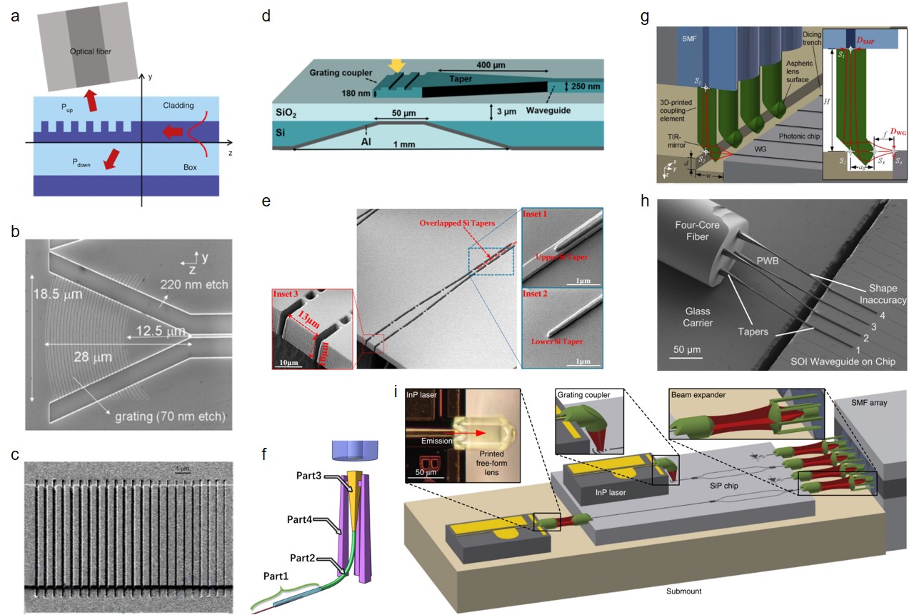
Grating coupler is one common such structure, which enlarges the mode size of the waveguide by etching diffraction gratings on the waveguide surface Taillaert2002 . The cross-section view of the uniform surface-corrugated grating structure is shown in Fig. 6a, and the picture of one fabricated grating coupler is shown in Fig. 6b. Typically, the grating couplers have an alignment tolerance value of 2m for 1 dB excess losses and over 20 nm 1 dB bandwidth. The relaxed spatial alignment tolerance facilitates multi-path alignment, which is one key part for scalable photonic information applications. Since quantum signals are difficult to be amplified, the losses should be reduced as much as possible. For the uniform grating structure, the grating couplers have a typical coupling efficiency of 5 dB Van2007 . To improve the coupling efficiency, different principles and techniques were introduced. One method is to spatially vary fill factors and etch depths (Fig. 6c), which can achieve larger overlap integral values between the field profiles of light from the grating coupler structure and the optical fiber Tang2010 ; Li2013 ; Benedikovic2014 ; Li2014 ; Marchetti2017 . These apodized grating couplers achieved a typical coupling efficiency of 1 dB. Considering that a substantial portion of the optical power input is lost in the substrate due to the diffraction downward from the grating structure (Fig. 6a), another rule is to improve the radiation directionality. Many techniques were developed, such as using overlay grating elements Vermeulen2010 and substrate metal mirrors (Fig. 6d) Hoppe2020 . Especially, one can improve both the overlap integral and directionality Taillaert2004 , and below 1 dB coupling loss was achieved in this way Ding2014 . It is worth mentioning that such high-efficiency grating couplers have been employed and played an important role in multi-photon quantum information processing on the silicon photonic circuits Paesani2019 ; Llewellyn2020 ; Vigliar2021 . The grating couplers are typically polarization dependent. In order to utilize polarization degree of freedom to encode quantum information, 2D grating couplers are alway used, which are able to couple orthogonal polarization of light into separate waveguides Xue2019 .
End coupler is another common structure for chip-fiber coupling. Designs of the tapered waveguide have been introduced to enlarge the effective mode size of the integrated silicon waveguides (Fig. 6e). Similar to grating couplers, the end couplers have also achieved below 1 dB coupling losses with commercial single mode fibers Pu2010 ; Fang2011 ; Jia2018 . In addition, the end couplers can achieve greater 1 dB bandwidth and support the simultaneous and efficient coupling of two polarization modes (Table IV). The locating on the chip edges facilitates direct packaging with the fiber array, despite requiring additional dedicated fabrication steps, such as chip dicing and polishing. Multi-channel packaging with end coupling has been demonstrated for deep learning Shen2017 and quantum transport simulations Harris2017 . Similar to end coupling, a three-dimensional (3D) fabricated polymer coupler showing coupling loss of 1 dB was demonstrated recently (Fig. 6f). Luo2020 .
In addition to fabricating complex coupling structures on chip, many other efficient approaches are also worth considering. For example, 3D-printed optical probes on the fiber end faces (Fig. 6g), which can realize the detection of vertical cutting edge devices, were recently demonstrated with 1.9 dB coupling loss Trappen2020 . Photonic wire bonding and in situ 3D nanoprinting are other novel and promising techniques for chip-scale multi-platform interconnects (Fig. 6h and 6i). Using polymer waveguides with 3D geometry, photonic wire bonding can bridge photonic circuits on different chips Lindenmann2012 ; Lindenmann2015 ; Billah2018 ; Rhee2022 . With this technique, 1.6 dB coupling loss between silicon chips Lindenmann2012 , 1.7 dB coupling loss between a four-core fiber and a silicon chip Lindenmann2015 and 0.4 dB coupling loss between an indium phosphide chip and a silicon photonic chip Billah2018 were demonstrated. In situ 3D nanoprinting technique exploits direct-write two-photon laser lithography to create ultracompact elements such as lenses and expanders, which can be directly integrated onto surfaces of optical integrated devices Dietrich2018 . These elements can be optimized according to the coupling objectives, thus increasing the flexibility. In ref. Dietrich2018 , coupling efficiencies of up to 0.6 dB between edge-emitting lasers and single-mode fibres and 2.5 dB between lasers and passive chips were achieved. Introducing these two new technologies into integrated quantum photonics will greatly improve the chip complexity and integration.
III. Scalable quantum information applications
After decades of development, silicon photonics has made a series of significant advances in quantum computing, quantum simulation, quantum communication and metrology, etc. Here we give a review of some important advances in recent years, and they are fundamental and have irreplaceable values in the extended applications of quantum information processing, including multiphoton and high-dimensional applications and quantum error correction on one single chip, and quantum key distribution and state teleportation among chips.
.6 A. Multiphoton and high-dimensional applications
Assuming that a system contains photons with dimension, the system capacity is . Therefore, increasing the number of photons will improve the system capacity exponentially, and it is vitally important. Although multiple solid-state quantum emitters can be integrated on the same chip and multiple determinate single photons can be generated, controlling emitters to ensure indistinguishability between photons remains a major difficulty. Through multiplexing techniques, single emitter can also generate multiple identical photons and complex quantum states Istrati2020 ; Wangw2017 , however, there are still difficulties in on-chip integration of multiplexing components. Alternative approach, SFWM can generate multiple photons directly on the single chip and the relevant work have made great progress in recent years.
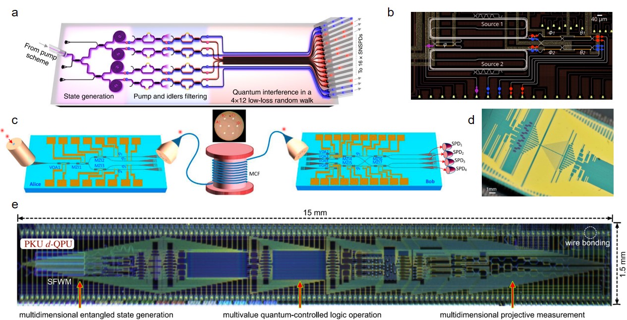
With strong third-order nonlinear response, silicon waveguides and micro-ring resonators have been used to generate entangled photon pairs with different degrees of freedom Feng2019 ; Takesue2007 ; Takesue2008 ; Matsuda2012 ; Silverstone2015 ; Li2017 and to demonstrate various optical quantum applications Wangwang2017 ; Paesani2017 ; Qiang2018 ; Qiang2021 . Furthermore, multiple photon pairs were multiplexed to generate quantum states consisted with more photons. In 2011, ref. Harada2011 has performed quantum interference experiment with two heralded photons generated in two independent silicon waveguides. A visibility of 73% has been observed. Later, in 2018, this multi-photon interference process has been demonstrated on one single chip with heralded photons from two independent micro-ring resonator sources and interference fringe visibility as 72% was measured Faruque2018 . Almost at the same time, silicon waveguides have been used to prepare complex four-photon states Zhang2019 and frequency-degenerate entangled four-photon states Feng20192 . These works stimulate more multi-photon applications in integrated optical chips, such as preparation of programmable four-photon graph states Adcock2019 , generation and sampling of quantum states of light (Fig. 7a) Paesani2019 and observing nonlocal quantum interference Feng2021 . So far, the number of photons on one single silicon chip has been increased to 8 Paesani2019 and more photons could be achieved by further reducing losses. In improving the quality of multi-photon interference, different strategies have been demonstrated to improve the spectral purity of photon pairs Paesani2020 ; Liu2020 ; Burridge2020 . In particular, ref. Paesani2020 has achieved on-chip heralded two-photon quantum interference with a visibility of 96% (Fig. 7b). These high-quality integrated photonic sources are promising in practical quantum applications.
High-dimensional encoding is another feasible approach to a larger system capacity. Moreover, it shows many unique quantum properties and provides improvements in particular applications such as higher capacity and noise robustness in quantum communications Hu2018 and higher efficiency and flexibility in quantum computing Lanyon2009 . On integrated chips, many degrees of freedom can be used for high-dimensional encoding, such as path, transverse-mode, frequency and time-bins. Among them, path encoding is the most common one due to its ease of implementation. With on-chip beam splitter and Mach-Zehnder interferometers, photons can be routed and manipulated in multiple paths. Coupled waveguide array also can be used to construct the desired dynamic evolution Hamiltonian for research including quantum walk, boson sampling and quantum simulation.
For high-dimensional quantum applications with integrated devices, ref. Ding2017 has experimentally demonstrated high-dimensional chip-to-chip quantum interconnection for the first time in 2017 (Fig. 7c). High-dimensional quantum information generated in one silicon photonic chip has been distributed to another chip through one multicore fiber. Combined with on-chip quantum photonic sources, programmable high-dimensional bipartite entangled systems have been realized Wang2018 ; Lu2020 . Recently, a programmable qudit-based quantum processor including all key functions for initialisation, manipulation, and measurement of two quantum quart states and multi-value quantum-controlled logic gates has been demonstrated on a silicon chip (Fig. 7e) Chi2022 .
Despite path, other degrees of freedom also have advantages in increasing the system capacity. For example, integrated photonic sources always have multiple frequencies Feng2020 and waveguide transverse-mode shows a compact way for parallel encoding Dai2018 . Furthermore, it is effective to use multiple degrees of freedom of a quantum particle simultaneously Feng2016 . The development of on-chip conversion devices will greatly increase the application prospects of these degrees of freedom.
.7 B. Quantum error correction
Despite many natural advantages, quantum information processor faces one basic difficulty, that is, the errors. When the product of logical operations and error rates of qubits reaches a certain level, the logical operations will loss their reliability. Meanwhile, due to quantum no-clone theorem, qubits cannot be copied, and eliminate errors by repetition as in classical processors is impossible. Therefore, effective quantum error correction is a necessary step to realize one realistic quantum processor. In photonic quantum technologies, photon loss, quality of quantum states, and imperfect logical operations are all sources of errors. Various schemes were developed to improving fault-tolerant capability with photons, such as making efforts for decreasing fabrication imperfections to obtain high-performance optical components. In ref. Wilkes2016 , 60 dB extinction ratio MZI can be achieved with improved design, which equivalently can implement single-qubit quantum gate with 99.9999% fidelity.
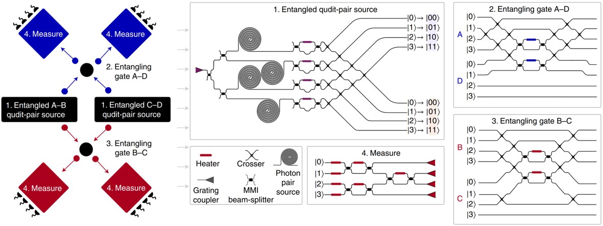
Another famous method is the generation of large-scale cluster states for measurement-based quantum computation (MBQC) Yao2012 ; Larsen2019 ; Asavanant2019 , which depends on a sequence of local measurements on a special entangled state, called the cluster or graph state. MBQC is equivalent to the circuit-based quantum computation model, and since it is relatively easy to prepare this kind of entangled states with nonlinear photonics, this model is highly valued in photonic quantum information applications. Besides being used in quantum computation, cluster state also shows important applications in other fields such as quantum error correction, multi-partite quantum communication and quantum metrology, as well as in the study of fundamental problems such as non-locality and decoherence Hein2006 ; Shettell2020 . So far, with silicon photonic circuits, all types of four-photon graph state have been programmably generated Adcock2019 , and a range of quantum information processing tasks with and without error-correction encodings have been implemented (Fig. 8) Vigliar2021 . The success rate was increased from 62.5% to 95.8% when running a phase-estimation algorithm by using the error-correction program. Similar to MBQC, fusion-based quantum computation was proposed and developed in recent years by PsiQuantum Bartolucci2021 ; Bombin2021 . With small-scale entangled photons as resource states and fusion-measurement, large-scale universal fault-tolerant quantum computing can be realized with on-chip components.
Other novel error-correction methods includes entanglement purification and topologically electromagnetic modes. Entanglement purification is a way to extract a subset of states of high entanglement and high purity from a large set of less entangled states, which can significantly increase the quality of logic operations between different qubits and relax the requirement for high-accuracy logic operations Pan2003 . The topologically electromagnetic modes are much less affected by nanophotonic fabrication-induced disorder and can be used to avoid errors. Up to now, topological quantum light sources Mittal2018 ; Wang2019 ; Dai2022 and quantum interference process Chenchen2021 on silicon photonic chips have been demonstrated.
.8 C. Quantum key distribution
Governed by the laws of quantum mechanics, quantum key distribution (QKD) aims to share information with absolute security between the transmitters and receivers. After decades of development, QKD is becoming the building block of quantum network, and many quantum encoding protocols have been developed, such as BB84, two-state and Einstein-Podolsky-Rosen protocol Gisin2002 . As the common choice of information carrier, photons are distributed over 803-km fiber Wangw2022 and from the satellite to the ground over a distance of up to 1,200 kilometres Liao2017 . For convenience and practicality purposes, transmitters and receivers have been integrated on the photonic chip to achieve dense integration, high stability and scalability Wang2021 , and are connected by single-mode or multicore fibers Ding2017 ; Sibson2017 ; Bacco2017 .
Through combining slow thermo-optic DC biases and fast (10 GHz bandwidth) carrier-depletion modulation, high-speed low-error QKD modulation has been achieved with silicon photonic devices Sibson2017 . Besides, QKD systems with integrated silicon photonics have been demonstrated in an intercity metropolitan test with a 43-km fiber Bunandar2017 and even full daylight Avesani2019 . The QKD system is becoming more compact and different degrees of freedom encoding have been implemented such as path Ding2017 , polarization Bunandar2017 and time-bins Beutel2021 ; Geng2019 . Based on hybrid techniques, photon lasers Agnesi2019 and photon detection processes Rafaelli2018 ; Beutel2021 ; Zheng2021 have been integrated directly on the silicon chip. The high-dimensional QKD with quantum states generated in the silicon photonic circuits enables surpassing the information efficiency limit of traditional quantum key distribution protocols Ding2017 . With these technological advances, different key distribution protocols have been achieved with integrated silicon photonic devices such as BB84 Sibson2017 , continuous-variable Zhangzhang2019 and measurement-device-independent Wei2020 , as shown in Fig. 9.
.9 D. Quantum state teleportation
Quantum state teleportation aims to transfer a particle’s quantum state to another particle rather than itself. As a new way of communication, this technique transfers quantum information carried in the quantum state with the help of quantum entanglement, and forms the basis of scalable quantum network and distributed quantum computing. It involves three particles (A, B, C), and we assume particle B and C are Bell entangled. The quantum state of particle A can be transferred to particle B through Bell state measurement between A and C. With quantum state teleportation, linear optical quantum information processor can be efficiently scaled by using a large number of cascaded gates Kok2007 .
The integrated quantum teleportation process was first implemented with silica slab waveguides Metcalf2014 , which was fabricated by the direct UV-writing technique. The silica waveguides have large cross-section (typically 4.5m4.5m), and low chip-fiber coupling loss and transmission loss enable us to achieve single photons generated in free-space feeding into the chip directly through optical fibers while maintaining high brightness. In ref. Metcalf2014 , four photons which were generated in free-space nonlinear crystals were used. Three photons were input into the chip, and the left one was input into the detector as heralding. On-chip interferometers were used to realize the functions of entanglement generation and Bell state measurement. Based on state measurement results, classical communications and corresponding quantum state operations, quantum state of one photon would be transferred to another photon.
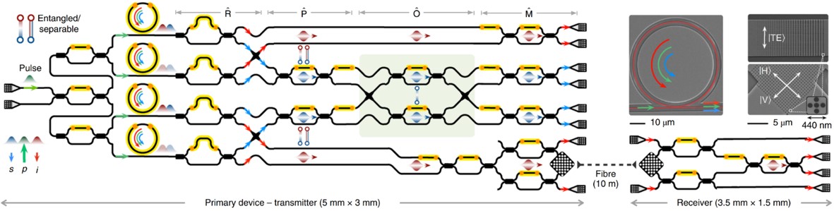
Of course, quantum teleportation process can be achieved with silicon waveguides. In particular, strong SFWM in silicon waveguides can be used directly to manipulate multi-photon entangled quantum states. In ref. Llewellyn2020 , quantum teleportation between two silicon chips have been demonstrated, as shown in Fig. 10. Four microresonators were used to generate high-quality entangled quantum states directly on the silicon chip. Before the validation of teleportation process, photons that obtained the quantum states were transmitted to another chip with quantum photonic interconnect by path-polarization interconversion Wang2016 , where quantum states were reconstructed via state tomography measurements. This achievement lays the foundation for large-scale integrated photon quantum technology in communication and computing.
IV. Challenges and outlook
Despite progress mentioned above, further improvements are needed in some areas for scalable quantum information applications. Below, we outline some challenges in silicon photonic quantum technologies.
Low-Loss Components: Loss is one huge challenge for optical quantum integrated systems, including loss of passive structures, delay lines, switches and chip interconnects. Because of the small effective mode area, loss in silicon is more prominent than in other materials, such as silica. Although the state-of-the-art low transmission loss of 0.08 dB/m has been demonstrated based on sidewall smoothing techniques Lee2012 , it is difficult to apply to waveguide structures with common strip waveguides. Multimode waveguide technology and mixing with silica or silicon nitride could enable the next generation of ultra low-loss components.
Photon Generation: For parametric photonic sources, the silicon waveguide has strong two-photon absorption at 1550 nm, and it is difficult to enhance the brightness of the photonic sources just through increasing the pump power. Besides, the properties of the photonic sources are relatively poor, especially for multi-photon interference. Photonic source capable of large-scale expansion with high brightness is still on the way. Extending photons to the far infrared band, where silicon has low two-photon absorption, is one potential method. Another possible solution is to develop hybrid integrated silicon chips with other materials with better nonlinear properties, such as silicon nitride, in which preparation of tens of photons has been demonstrated Arrazola2021 , and lithium niobate, which has strong second-order nonlinear response. The stochastic character of the photon sources needs to be solved, and multiplexed photon sources, long-time delay and high-speed modulation should be integrated totally on the same chip. For deterministic single-photon sources, modulation to increase the indistinguishability between different sources should be developed.
Deterministic Quantum Operation: The negligible photon-photon interaction limits the applicability of many photon-based schemes. To overcome this limitation, multiplexed photon sources and feedforward capability based on heralded detection of auxiliary photons should be integrated totally on the same chip. Strong nonlinear media such as atoms need to be introduced into the chip to enhance the photon-photon interaction to build deterministic multi-photon gates.
Frequency Conversion: Efficient frequency conversion will link various quantum systems to build up quantum networks, such as photonic conversion between microwave and telecom C-band. Efficient conversion at the single-photon level will allow us to take advantage of different systems, even if they are far away.
We have witnessed tremendous advances in silicon photonic devices for quantum information processing, especially in recent years. Photon source, quantum state manipulation and detection can be integrated on a chip and hopefully on the same chip, and integrated programmable multi-photon and high-dimensional quantum information processors have been demonstrated. With the further upgrading of fabrication technology, silicon photonics will have a greater prospect in quantum information processing. Of course, silicon photonic devices still face many defects of the material itself, and the future quantum information processors are most likely to be hybrid with various materials elevated to the extreme. In any case, we believe that silicon photonics will play an important role.
Funding. This work was supported by the National Natural Science Foundation of China (NSFC) (Nos. 62061160487, 62005239, 12004373, 61974168, 62075243), the Innovation Program for Quantum Science and Technology (No. 2021ZD0303200), the Natural Science Foundation of Zhejiang Province (LQ21F050006), the National Key Research and Development Program (2017YFA0305200), the Key Research and Development Program of Guangdong Province of China (2018B030329001 and 2018B030325001), the Postdoctoral Science Foundation of China (No. 2021T140647) and the Fundamental Research Funds for the Central Universities. This work was partially carried out at the USTC Centre for Micro and Nanoscale Research and Fabrication.
Disclosures. The authors declare no conflicts of interest.
References
- (1) C. H. Bennett, and G. Brassard, “Quantum cryptography: Public key distribution and coin tossing,” In: Proceedings of the International Conference on Computers, Systems and Signal Processing 175–179 (1984).
- (2) N. Gisin, G. Ribordy, W. Tittel, and H. Zbinden, “Quantum cryptography,” Rev. Mod. Phys. 79, 145–195 (2002).
- (3) P. W. Shor, “Polynomial-time algorithms for prime factorization and discrete logarithms on a quantum computer,” SIAM review 41, 303–332 (1999).
- (4) L. K. Grover, “Quantum mechanics helps in searching for a needle in a haystack,” Phys. Rev. Lett. 79, 325–328 (1997).
- (5) R. P. Feynman, “Simulating physics with computers,” Internat. J. Theoret. Phys. 21, 467–488 (1982).
- (6) V. Giovannetti, S. Lloyd, and L. Maccone, “Advances in quantum metrology,” Nature Photon. 5, 222–229 (2011).
- (7) F. Arute, K. Arya, R. Babbush, et al., “Quantum supremacy using a programmable superconducting processor,” Nature 574, 505–510 (2019).
- (8) H. S. Zhong, H. Wang, Y. H. Deng, et al., “Quantum computational advantage using photons,” Science 370, 1460–1463 (2020).
- (9) Y. Wu, W. S. Bao, S. Cao, et al., “Strong quantum computational advantage using a superconducting quantum processor,” Phys. Rev. Lett. 127, 180501 (2021).
- (10) S. K. Liao, W. Q. Cai, W. Y. Liu, et al., “Satellite-to-ground quantum key distribution,” Nature 549, 43–47 (2017).
- (11) B. P. Abbott, R. Abbott, T. D. Abbott, et al., “Observation of gravitational waves from a binary black hole merger,” Phys. Rev. Lett. 116, 061102 (2016).
- (12) J. M. Boss, K. S. Cujia, J. Zopes, and C. L. Degen, “Quantum sensing with arbitrary frequency resolution,” Science 356, 837–840 (2017).
- (13) Y. Zheng, L. M. Zhou, Y. Dong, C. W. Qiu, X. D. Chen, G. C. Guo, and F. W. Sun, “Robust optical-levitation-based metrology of nanoparticle’s position and mass,” Phys. Rev. Lett. 124, 223603 (2020).
- (14) J. L. O’brien, A. Furusawa, and J. Vučković, “Photonic quantum technologies,” Nature Photon. 3, 687–695 (2009).
- (15) F. Flamini, N. Spagnolo, and F. Sciarrino, “Photonic quantum information processing: a review,” Rep. Prog. Phys. 82, 016001 (2018).
- (16) S. Slussarenko, and G. J. Pryde, “Photonic quantum information processing: A concise review,” Appl. Phys. Rev. 6, 041303 (2019).
- (17) J. Wang, F. Sciarrino, A. Laing, and M. G. Thompson, “Integrated photonic quantum technologies,” Nature Photon. 14, 273–284 (2020).
- (18) L. Lu, X. Zheng, Y. Lu, S. Zhu, and X. S. Ma, “Advances in chip-scale quantum photonic technologies,” Adv. Quantum Tech. 4, 2100068 (2021).
- (19) A. Politi, M. J. Cryan, J. G. Rarity, S. Yu, and J. L. O’Brien, “Silica-on-silicon waveguide quantum circuits,” Science 320, 646–649 (2008).
- (20) X. Jiang, L. Shao, S. X. Zhang, X. Yi, J. Wiersig, L. Wang, Q. Gong, M. Lončar, L. Yang, and Y. F. Xiao, “Chaos-assisted broadband momentum transformation in optical microresonators,” Science 358, 344–347 (2017).
- (21) X. Zhang, Q. T. Cao, Z. Wang, Y. x. Liu, C. W. Qiu, L. Yang, Q. Gong, and Y. F. Xiao, “Symmetry-breaking-induced nonlinear optics at a microcavity surface,” Nature Photon. 13, 21–24 (2019).
- (22) M. Li, C. Li, Y. Chen, L. T. Feng, L. Yan, Q. Zhang, J. Bao, B. H. Liu, X. F. Ren, J. Wang, S. Wang, Y. G, X. Hu, Q. Gong, Y. Li, “On-chip path encoded photonic quantum Toffoli gate,” Photonics Res. 10, 07001533 (2022).
- (23) J. W. Silverstone, D. Bonneau, J. L. O’Brien, and M. G. Thompson, “Silicon quantum photonics,” IEEE J. Sel. Topics Quantum Electron. 22, 390–402 (2016).
- (24) X. Zhang, B. A. Bell, A. Mahendra, C. Xiong, P. H. W. Leong, and B. J. Eggleton, “Integrated silicon nitride time-bin entanglement circuits,” Opt. Lett. 43, 3469–3472 (2018).
- (25) X. Lu, Q. Li, D. A. Westly, G. Moille, A. Singh, V. Anant, and K. Srinivasan, “Chip-integrated visible-telecom entangled photon pair source for quantum communication,” Nat. Phys. 15, 373–381 (2019).
- (26) C. Taballione, R. van der Meer, H. J. Snijders, P. Hooijschuur, J. P. Epping, M. de Goede, B. Kassenberg, P. Venderbosch, C. Toebes, H. van den Vlekkert, P. W. H. Pinkse, and J. J. Renema, “A universal fully reconfigurable 12-mode quantum photonic processor,” Mater. Quantum. Technol. 1, 035002 (2021).
- (27) S. Y. Ren, W. Yan, L. T. Feng, Y. Chen, Y. K. Wu, X. Z. Qi, X. J. Liu, Y. J. Cheng, B. Y. Xu, L. J. Deng, G. C. Guo, L. Bi, and X. F. Ren, “Single-photon nonreciprocity with an integrated magneto-optical isolator,” Laser Photonics Rev. 16, 2100595 (2022).
- (28) H. Jin, F. M. Liu, P. Xu, J. L. Xia, M. L. Zhong, Y. Yuan, J. W. Zhou, Y. X. Gong, W. Wang, and S. N. Zhu, “On-chip generation and manipulation of entangled photons based on reconfigurable lithium-niobate waveguide circuits,” Phys. Rev. Lett. 113, 103601 (2014).
- (29) C. Wang, X. Xiong, N. Andrade, V. Venkataraman, X. F. Ren, G. C. Guo, and M. Lončar, “Second harmonic generation in nano-structured thin-film lithium niobate waveguides,” Opt. Express 25, 6963–6973 (2017).
- (30) B. Y. Xu, L. Chen, J. Lin, L. T. Feng, R. Niu, Z. Y. Zhou, R. Gao, C. Dong, G. Guo, Q. Gong, Y. Cheng, Y. F. Xiao, and X. F. Ren, “Spectrally multiplexed and bright entangled photon pairs in a lithium niobate microresonator,” Sci. China-Phys. Mech. Astron. 65, 294262 (2022).
- (31) R. J. Bojko, J. Li, L. He, T. Baehr-Jones, and M. Hochberg, “Electron beam lithography writing strategies for low loss, high confinement silicon optical waveguides,” J. Vac. Sci. Technol. B 29, 06F309 (2011).
- (32) K. Sugioka, and Y. Cheng, “Ultrafast lasers-reliable tools for advanced materials processing,” Light Sci. Appl. 3, e149 (2014).
- (33) T. Rudolph, “Why I am optimistic about the silicon-photonic route to quantum computing,” APL Photon. 2, 030901 (2017).
- (34) D. Thomson, A. Zilkie, J. E. Bowers, T. Komljenovic, G. T. Reed, L. Vivien, D. Marris-Morini, E. Cassan, L. Virot, J. M. Fédéli, J. M. Hartmann, J. H Schmid, D. X. Xu, F. Boeuf, P. O’Brien, G. Z Mashanovich, and M. Nedeljkovic, “Roadmap on silicon photonics,” J. Opt. 18, 073003 (2016).
- (35) G. Son, S. Han, J. Park, K. Kwon, and K. Yu, “High-efficiency broadband light coupling between optical fibers and photonic integrated circuits,” Nanophotonics 7, 1845–1864 (2018).
- (36) N. C. Harris, D. Bunandar, M. Pant, G. R. Steinbrecher, J. Mower, M. Prabhu, T. Baehr-Jones, M. Hochberg, and D. Englund, “Large-scale quantum photonic circuits in silicon,” Nanophotonics 5, 456–468 (2016).
- (37) W. H. Pernice, C. Schuck, O. Minaeva, M. Li, G. N. Goltsman, A. V. Sergienko, and H. X. Tang, “High-speed and high-efficiency travelling wave single-photon detectors embedded in nanophotonic circuits,” Nat. Commun. 3, 1325 (2012).
- (38) L. T. Feng, G. C. Guo, and X. F. Ren, “Progress on integrated quantum photonic sources with silicon,” Adv. Quantum Tech. 3, 1900058 (2020).
- (39) X. Chen, Z. Fu, Q. Gong, and J. Wang, “Quantum entanglement on photonic chips: a review,” Adv. Photon. 3, 064002 (2021).
- (40) J. C. Adcock, J. Bao, Y. Chi, X. Chen, D. Bacco, Q. Gong, L. K. Oxenløwe, J. Wang, and Y. Ding, “Advances in silicon quantum photonics,” IEEE J. Sel. Top. Quantum Electron. 27, 6700224 (2020).
- (41) A. W. Elshaari, W. Pernice, K. Srinivasan, O. Benson, and V. Zwiller, “Hybrid integrated quantum photonic circuits,” Nature Photon. 14, 285–298 (2020).
- (42) J. H. Kim, S. Aghaeimeibodi, J. Carolan, D. Englund, and E. Waks, “Hybrid integration methods for on-chip quantum photonics,” Optica 7, 291–308 (2020).
- (43) Y. H. Li, Z. Y. Zhou, L. T. Feng, W. T. Fang, S. L. Liu, S. K. Liu, K. Wang, X. F. Ren, D. S. Ding, L. X. Xu, and B. S. Shi, “On-chip multiplexed multiple entanglement sources in a single silicon nanowire,” Phys. Rev. Appl. 7, 064005 (2017).
- (44) C. Ma, X. Wang, V. Anant, A. D. Beyer, M. D. Shaw, and S. Mookherjea, “Silicon photonic entangled photon-pair and heralded single photon generation with and ,” Opt. Express 25, 32995–33006 (2017).
- (45) Y. Liu, C. Wu, X. Gu, Y. Kong, X. Yu, R. Ge, X. Cai, X. Qiang, J. Wu, X. Yang, and P. Xu, “High-spectral-purity photon generation from a dual-interferometer-coupled silicon microring,” Opt. Lett. 45, 73–76 (2020).
- (46) B. M. Burridge, I. I. Faruque, J. G. Rarity, and J. Barreto, “High spectro-temporal purity single-photons from silicon micro-racetrack resonators using a dual-pulse configuration,” Opt. Lett. 45, 4048–4051 (2020).
- (47) S. Paesani, M. Borghi, S. Signorini, A. Maïnos, L. Pavesi, and A. Laing, “Near-ideal spontaneous photon sources in silicon quantum photonics,” Nat. Commun. 11, 2505 (2020).
- (48) M. J. Collins, C. Xiong, I. H. Rey, T. D. Vo, J. He, S. Shahnia, C. Reardon, T. F. Krauss, M. J. Steel, A. S. Clark, and B. J. Eggleton, “Integrated spatial multiplexing of heralded single-photon sources,” Nat. Commun. 4, 2582 (2013).
- (49) X. Zhang, I. Jizan, J. He, A. S. Clark, D.-Y. Choi, C. J. Chae, B. J. Eggleton, and C. Xiong, “Enhancing the heralded single-photon rate from a silicon nanowire by time and wavelength division multiplexing pump pulses,” Opt. Lett. 40, 2489–2492 (2015).
- (50) C. Xiong, X. Zhang, Z. Liu, M. J. Collins, A. Mahendra, L. G. Helt, M. J. Steel, D. -Y. Choi, C. J. Chae, P. H. W. Leong, and B. J. Eggleton, “Active temporal multiplexing of indistinguishable heralded single photons,” Nat. Commun. 7, 10853 (2016).
- (51) F. Kaneda, and P. G. Kwiat, “High-efficiency single-photon generation via large-scale active time multiplexing,” Sci. Adv. 5, eaaw8586 (2019).
- (52) H. Lee, T. Chen, J. Li, O. Painter, and K. J. Vahala, “Ultra-low-loss optical delay line on a silicon chip,” Nat. Commun. 3, 867 (2012).
- (53) M. He, M. Xu, Y. Ren, J. Jian, Z. Ruan, Y. Xu, S. Gao, S. Sun, X. Wen, L. Zhou, L. Liu, C. Guo, H. Chen, S. Yu, L. Liu, and X. Cai, “High-performance hybrid silicon and lithium niobate Mach–Zehnder modulators for 100 Gbit s-1 and beyond,” Nat. Photonics 13, 359–364 (2019).
- (54) S. Haffouz, K. D. Zeuner, D. Dalacu, P. J. Poole, J. Lapointe, D. Poitras, K. Mnaymneh, X. Wu, M. Couillard, M. Korkusinski, E. Schöll, K. D. Jöns, V. Zwiller, and R. L. Williams, “Bright single InAsP quantum dots at telecom wavelengths in position-controlled InP nanowires: the role of the photonic waveguide,” Nano Lett. 18, 3047–3052 (2018).
- (55) J. H. Kim, S. Aghaeimeibodi, C. J. Richardson, R. P. Leavitt, D. Englund, and E. Waks, “Hybrid integration of solid-state quantum emitters on a silicon photonic chip,” Nano Lett. 17, 7394–7400 (2017).
- (56) T. Müller, J. Skiba-Szymanska, A. B. Krysa, J. Huwer, M. Felle, M. Anderson, R. M. Stevenson, J. Heffernan, D. A. Ritchie, and A. J. Shields, “A quantum light-emitting diode for the standard telecom window around 1,550 nm,” Nat. Commun. 9, 862 (2018).
- (57) R. Katsumi, Y. Ota, M. Kakuda, S. Iwamoto, and Y. Arakawa, “Transfer-printed single-photon sources coupled to wire waveguides,” Optica 5, 691–694 (2018).
- (58) R. Katsumi, Y. Ota, A. Osada, T. Yamaguchi, T. Tajiri, M. Kakuda, S. Iwamoto, H. Akiyama, and Y. Arakawa, “Quantum-dot single-photon source on a CMOS silicon photonic chip integrated using transfer printing,” APL Photon. 4, 036105 (2019).
- (59) Y. Zhou, Z, Wang, A. Rasmita, S. Kim, A. Berhane, Z. Bodrog, G. Adamo, A. Gali, I. Aharonovich, and W. B. Gao, “Room temperature solid-state quantum emitters in the telecom range,” Sci. Adv. 4, eaar3580 (2018).
- (60) H. Zhao, M. T. Pettes, Y. Zheng, and H. Htoon, “Site-controlled telecom-wavelength single-photon emitters in atomically-thin MoTe2,” Nat. Commun. 12, 6753 (2021).
- (61) W. Redjem, A. Durand, T. Herzig, A. Benali, S. Pezzagna, J. Meijer, A. Yu. Kuznetsov, H. S. Nguyen, S. Cueff, J.-M. Gérard, I. Robert-Philip, B. Gil, D. Caliste, P. Pochet, M. Abbarchi, V. Jacques, A. Dréau, and G. Cassabois, “Single artificial atoms in silicon emitting at telecom wavelengths,” Nat. Electron. 3, 738–743 (2020).
- (62) M. Hollenbach, Y. Berencén, U. Kentsch, M. Helm, and G. V. Astakhov, “Engineering telecom single-photon emitters in silicon for scalable quantum photonics,” Opt. Express 28, 26111–26121 (2020).
- (63) L. Bergeron, C. Chartrand, A. T. K. Kurkjian, K. J. Morse, H. Riemann, N. V. Abrosimov, P. Becker, H. J. Pohl, M. L. W. Thewalt, and S. Simmons, “Silicon-integrated telecommunications photon-spin interface,” PRX Quantum 1, 020301 (2020).
- (64) D. B. Higginbottom, A. T. K. Kurkjian, C. Chartrand, et al., “Optical observation of single spins in silicon,” Nature 607, 266–270 (2022).
- (65) M. Hollenbach, N. S. Jagtap, C. Fowley, J. Baratech, V. Guardia-Arce, U. Kentsch, A. Eichler-Volf, N. V. Abrosimov, A. Erbe, C. Shin, H. Kim, M. Helm, W. Lee, G. V. Astakhov, and Y. Berencén, “A photonic platform hosting telecom photon emitters in silicon,” arXiv preprint arXiv:2112.02680, 2021.
- (66) M. Prabhu, C. Errando-Herranz, L. D. Santis, I. Christen, C. Chen, and D. R. Englund, “Individually addressable artificial atoms in silicon photonics,” arXiv preprint arXiv:2202.02342, 2022.
- (67) S. Liu, K. Srinivasan, and J. Liu, “Nanoscale positioning approaches for integrating single solid-state quantum emitters with photonic nanostructures,” Laser Photonics Rev. 15, 2100223 (2021).
- (68) P. Peng, Y. C. Liu, D. Xu, Q. T. Cao, G. Lu, Q. Gong, and Y. F. Xiao, “Enhancing coherent light-matter interactions through microcavity-engineered plasmonic resonances,” Phys. Rev. Lett. 119, 233901 (2017).
- (69) S. Liu, Y. Wei, X. Li, Y. Yu, J. Liu, S. Yu, and X. Wang, “Dual-resonance enhanced quantum light-matter interactions in deterministically coupled quantum-dot-micropillars,” Light Sci. Appl. 10, 158 (2021).
- (70) Y. Wei, S. Liu, X. Li, Y. Yu, X. Su, S. Li, X. Shang, H. Liu, H. Hao, H. Ni, S. Yu, Z. Niu, J. Iles-Smith, J. Liu, and X. Wang, “Tailoring solid-state single-photon sources with stimulated emissions,” Nat. Nanotechnol. 17, 470–476 (2022).
- (71) R. B. Patel, A. J. Bennett, I. Farrer, C. A. Nicoll, D. A. Ritchie, and A. J. Shields, “Two-photon interference of the emission from electrically tunable remote quantum dots,” Nature Photon. 4, 632–635 (2010).
- (72) E. B. Flagg, A. Muller, S. V. Polyakov, A. Ling, A. Migdall, and G. S. Solomon, “Interference of single photons from two separate semiconductor quantum dots,” Phys. Rev. Lett. 104, 137401 (2010).
- (73) A. W. Elshaari, E. Büyüközer, I. E. Zadeh, T. Lettner, P. Zhao, E. Schöll, S. Gyger, M. E. Reimer, D. Dalacu, P. J. Poole, K. D. Jöns, and V. Zwiller, “Strain-tunable quantum integrated photonics,” Nano Lett. 18, 7969–7976 (2018).
- (74) B. Machielse, S. Bogdanovic, S. Meesala, S. Gauthier, M. J. Burek, G. Joe, M. Chalupnik, Y. I. Sohn, J. Holzgrafe, R. E. Evans, C. Chia, H. Atikian, M. K. Bhaskar, D. D. Sukachev, L. Shao, S. Maity, M. D. Lukin, and M. Lončar, “Quantum interference of electromechanically stabilized emitters in nanophotonic devices,” Phys. Rev. X 9, 031022 (2019).
- (75) R. Katsumi, Y. Ota, A. Osada, T. Tajiri, T. Yamaguchi, M. Kakuda, S. Iwamoto, H. Akiyama, and Y. Arakawa, “In situ wavelength tuning of quantum-dot single-photon sources integrated on a CMOS-processed silicon waveguide,” Appl. Phys. Lett. 116, 041103 (2020).
- (76) L. Zhai, G. N. Nguyen, C. Spinnler, J. Ritzmann, M. C. Löbl, A. D. Wieck, A. Ludwig, A. Javadi, and R. J. Warburton, “Quantum interference of identical photons from remote GaAs quantum dots,” Nat. Nanotechnol. (2022).
- (77) N. H. Wan, T.-J. Lu, K. C. Chen, M. P. Walsh, M. E. Trusheim, L. D. Santis, E. A. Bersin, I. B. Harris, S. L. Mouradian, I. R. Christen, E. S. Bielejec, and D. Englund, “Large-scale integration of artificial atoms in hybrid photonic circuits,” Nature 583, 226–231 (2020).
- (78) D. Benedikovic, L. Virot, G. Aubin, F. Amar, B. Szelag, B. Karakus, J.-M. Hartmann, C. Alonso-Ramos, X. L. Roux, P. Crozat, E. Cassan, D. Marris-Morini, C. Baudot, F. Boeuf, J.-M. Fédéli, C. Kopp, and L. Vivien, “25 Gbps low-voltage hetero-structured silicon-germanium waveguide pin photodetectors for monolithic on-chip nanophotonic architectures,” Photonics Res. 7, 437–444 (2019).
- (79) F. Raffaelli, G. Ferranti, D. H. Mahler, P. Sibson, J. E. Kennard, A. Santamato, G. Sinclair, D. Bonneau, M. G. Thompson, and J. C. F. Matthews, “A homodyne detector integrated onto a photonic chip for measuring quantum states and generating random numbers,” Quantum Sci. Technol. 3, 025003 (2018).
- (80) J. F. Tasker, J. Frazer, G. Ferranti, E. J. Allen, L. F. Brunel, S. Tanzilli, V. D’Auria, and J. C. F. Matthews, “Silicon photonics interfaced with integrated electronics for 9 GHz measurement of squeezed light,” Nat. Photonics 15, 11–15 (2021).
- (81) C. Bruynsteen, M. Vanhoecke, J. Bauwelinck, and X. Yin, “Integrated balanced homodyne photonic–electronic detector for beyond 20 GHz shot-noise-limited measurements,” Optica 8, 1146–1152 (2021).
- (82) D. V. Reddy, R. R. Nerem, S. W. Nam, R. P. Mirin, and V. B. Verma, “Superconducting nanowire single-photon detectors with 98% system detection efficiency at 1550 nm,” Optica 7, 1649–1653 (2020).
- (83) B. Korzh, Q. Y. Zhao, J. P. Allmaras, et al., “Demonstration of sub-3 ps temporal resolution with a superconducting nanowire single-photon detector,” Nat. Photonics 14, 250–255 (2020).
- (84) M. Akhlaghi, E. Schelew, and J. Young, “Waveguide integrated superconducting single-photon detectors implemented as near-perfect absorbers of coherent radiation,” Nat. Commun. 6, 8233 (2015).
- (85) J. Li, R. A. Kirkwood, L. J. Baker, D. Bosworth, K. Erotokritou, A. Banerjee, R. M. Heath, C. M. Natarajan, Z. H. Barber, M. Sorel, and R. H. Hadfield, “Nano-optical single-photon response mapping of waveguide integrated molybdenum silicide (MoSi) superconducting nanowires,” Opt. Express 24, 13931–13938 (2016).
- (86) S. Buckley, J. Chiles, A. N. McCaughan, G. Moody, K. L. Silverman, M. J. Stevens, R. P. Mirin, S. W. Nam, J. M. Shainline, “All-silicon light-emitting diodes waveguide-integrated with superconducting single-photon detectors,” Appl. Phys. Lett. 111, 141101 (2017).
- (87) A. Vetter, S. Ferrari, P. Rath, R. Alaee, O. Kahl, V. Kovalyuk, S. Diewald, G. N. Goltsman, A. Korneev, C. Rockstuhl, and W. H. P. Pernice, “Cavity-enhanced and ultrafast superconducting single-photon detectors,” Nano Lett. 16, 7085–7092 (2016).
- (88) J. Münzberg, A. Vetter, F. Beutel, W. Hartmann, S. Ferrari, W. H. P. Pernice, and C. Rockstuhl, “Superconducting nanowire single-photon detector implemented in a 2D photonic crystal cavity,” Optica 5, 658–665 (2018).
- (89) C. Cahall, K. L. Nicolich, N. T. Islam, G. P. Lafyatis, A. J. Miller, D. J. Gauthier, and J. Kim, “Multi-photon detection using a conventional superconducting nanowire single-photon detector,” Optica 4, 1534–1535 (2017).
- (90) D. Zhu, Q. Y. Zhao, H. Choi, T. J. Lu, A. E. Dane, D. Englund, and K. K. Berggren, “A scalable multi-photon coincidence detector based on superconducting nanowires,” Nature Nanotech. 13, 596–601 (2018).
- (91) D. Zhu, M. Colangelo, C. Chen, B. A. Korzh, F. N. C. Wong, M. D. Shaw, and K. K. Berggren, “Resolving photon numbers using a superconducting nanowire with impedance-matching taper,” Nano Lett. 20, 3858–3863 (2020).
- (92) Q. Y. Zhao, D. Zhu, N. Calandri, A. E. Dane, A. N. McCaughan, F. Bellei, H. Z. Wang, D. F. Santavicca, and K. K. Berggren, “Single-photon imager based on a superconducting nanowire delay line,” Nature Photon. 11, 247–251 (2017).
- (93) E. E. Wollman, V. B. Verma, A. E. Lita, W. H. Farr, M. D. Shaw, R. P. Mirin, and S. W. Nam, “Kilopixel array of superconducting nanowire single-photon detectors,” Opt. Express 27, 35279–35289 (2019).
- (94) R. Cheng, C. L. Zou, X. Guo, S. Wang, X. Han, and H. X. Tang, “Broadband on-chip single-photon spectrometer,” Nat. Commun. 10, 4104 (2019).
- (95) F. Beutel, H. Gehring, M. A. Wolff, C. Schuck, and W. Pernice, “Detector-integrated on-chip QKD receiver for GHz clock rates,” npj Quantum Inf. 7, 40 (2021).
- (96) X. Zheng, P. Zhang, R. Ge, L. Lu, G. He, Q. Chen, F. Qu, L. Zhang, X. Cai, Y. Lu, S. N. Zhu, P. Wu, and X. Ma, “Heterogeneously integrated, superconducting silicon-photonic platform for measurement-device-independent quantum key distribution,” Adv. Photon. 3, 055002 (2021).
- (97) P. Vines, K. Kuzmenko, J. Kirdoda, D. C. S. Dumas, M. M. Mirza, R. W. Millar, D. J. Paul, and G. S. Buller, “High performance planar germanium-on-silicon single-photon avalanche diode detectors,” Nat. Commun. 10, 1086 (2019).
- (98) L. F. Llin, J. Kirdoda, F. Thorburn, L. L. Huddleston, Z. M. Greener, K. Kuzmenko, P. Vines, D. C. S. Dumas, R. W. Millar, G. S. Buller, and D. J. Paul, “High sensitivity Ge-on-Si single-photon avalanche diode detectors,” Opt. Lett. 45, 6406–6409 (2020).
- (99) J. Zhang, M. A. Itzler, H. Zbinden, and J. W. Pan, “Advances in InGaAs/InP single-photon detector systems for quantum communication,” Light: Sci. Appl. 4, 286 (2015).
- (100) Y. Q. Fang, W. Chen, T. H. Ao, C. Liu, L. Wang, X. J. Gao, J. Zhang, and J. W. Pan, “InGaAs/InP single-photon detectors with 60% detection efficiency at 1550 nm,” Review of Scientific Instruments 91, 083102 (2020).
- (101) H. Wang, J. Guo, J. Miao, W. Luo, Y. Gu, R. Xie, F. Wang, L. Zhang, P. Wang, and W. Hu, “Emerging single-photon detectors based on low-dimensional materials,” Small 18, 2103963 (2022).
- (102) W. Song, R. Gatdula, S. Abbaslou, M. Lu, A. Stein, W. Y-C Lai, J. Provine, R. F. W. Pease, D. N. Christodoulides, and W. Jiang, “High-density waveguide superlattices with low crosstalk,” Nat. Commun. 6, 7027 (2015).
- (103) M. Zhang, L. T. Feng, M. Li, Y. Chen, L. Zhang, D. He, G. Guo, G. Guo, X. Ren, and D. Dai, “Supercompact photonic quantum logic gate on a silicon chip,” Phys. Rev. Lett. 126, 130501 (2021).
- (104) H. Zhou, Y. Wang, X. Gao, D. Gao, J. Dong, D. Huang, F. Li, P. A. Wai, and X. Zhang, “Dielectric metasurfaces enabled ultradensely integrated multidimensional optical system,” Laser Photonics Rev. 16, 2100521 (2022).
- (105) F. Horst, W. M. J. Green, S. Assefa, S. M. Shank, Y. A. Vlasov, and B. J. Offrein, “Cascaded Mach-Zehnder wavelength filters in silicon photonics for low loss and flat pass-band WDM (de-)multiplexing,” Opt. Express 21, 11652–11658 (2013).
- (106) S. Cheung, T. H. Su, K. Okamoto, S. J. B. Yoo, “Ultra-compact silicon photonic 512×512 25 GHz arrayed waveguide grating router,” IEEE J. Sel. Top. Quant. 20, 310–316 (2014).
- (107) D. T. H. Tan, A. Grieco, and Y. Fainman, “Towards 100 channel dense wavelength division multiplexing with 100 GHz spacing on silicon,” Opt. Express 22, 10408–10415 (2014).
- (108) S. T. Chen, X. Fu, J. Wang, Y. C. Shi, S. L. He, D. X. Dai, “Compact dense wavelength-division (De)multiplexer utilizing a bidirectional arrayed-waveguide grating integrated with a Mach-Zehnder interferometer,” J. Lightwave Technol. 33, 2279–2285 (2015).
- (109) D. Munk, M. Katzman, Y. Kaganovskii, N. Inbar, A. Misra, M. Hen, M. Priel, M. Feldberg, M. Tkachev, A. Bergman, M. Vofsi, M. Rosenbluh, T. Schneider, and A. Zadok, “Eight-channel silicon-photonic wavelength division multiplexer with 17 GHz spacing,” IEEE J. Sel. Topics Quantum Electron. 25, 8300310 (2019).
- (110) Z. Liu, J. Zhang, X. Li, L. Wang, J. Li, C. Xue, J. An, and B. Cheng, “25×50 Gbps wavelength division multiplexing silicon photonics receiver chip based on a silicon nanowire-arrayed waveguide grating,” Photon. Res. 7, 659–663 (2019).
- (111) A. B. Price, P. Sibson, C. Erven, J. G. Rarity, and M. G. Thompson, “High-speed quantum key distribution with wavelength-division multiplexing on integrated photonic devices,” in Conference on Lasers and Electro-Optics, OSA Terchnical Digest, JTh2A.24 (2018).
- (112) D. Liu, H. Xu, Y. Tan, Y. Shi, and D. Dai, “Silicon photonic filters,” Microw. Opt. Techn. Let. 63, 2252–2268 (2021).
- (113) S. Liao, Y. Ding, C. Peucheret, T. Yang, J. Dong, and X. Zhang, “Integrated programmable photonic filter on the silicon-on-insulator platform,” Opt. Express 22, 31993–31998 (2014).
- (114) F. Xia, M. Rooks, L. Sekaric, and Y. Vlasov, “Ultra-compact high order ring resonator filters using submicron silicon photonic wires for on-chip optical interconnects,” Opt. Express 15, 11934–11941 (2007).
- (115) J. R. Ong, R. Kumar, S. Mookherjea, “Ultra-high-contrast and tunable-bandwidth filter using cascaded high-order silicon micro-ring filters,” IEEE Photonic Tech. L. 25, 1543–1546 (2013).
- (116) P. Chen, S. Chen, X. Guan, Y. Shi, and D. Dai, “High-order microring resonators with bent couplers for a box-like filter response,” Opt. Lett. 39, 6304–6307 (2014).
- (117) D. Liu, C. Zhang, D. Liang, and D. Dai, “Submicron-resonator-based add-drop optical filter with an ultra-large free spectral range,” Opt. Express 27, 416–422 (2019).
- (118) H. Qiu, J. Jiang, T. Hu, P. Yu, J. Yang, X. Jiang, and H. Yu, “Silicon add-drop filter based on multimode bragg sidewall gratings and adiabatic couplers,” J. Lightwave Technol. 35, 1705–1709 (2017).
- (119) N. C. Harris, D. Grassani, A. Simbula, M. Pant, M. Galli, T. Baehr-Jones, M. Hochberg, D. Englund, D. Bajoni, and C. Galland, “Integrated source of spectrally filtered correlated photons for large-scale quantum photonic systems,” Phys. Rev. X 4, 041047 (2014).
- (120) D. Oser, S. Tanzilli, F. Mazeas, C. Alonso-Ramos, X. L. Roux, G. Sauder, X. Hua, O. Alibart, L. Vivien, É. Cassan, and L. Labonté, “High-quality photonic entanglement out of a stand-alone silicon chip,” npj Quantum Inf. 6, 31 (2020).
- (121) C. Li, D. Liu, and D. Dai, “Multimode silicon photonics,” Nanophotonics 8, 227–247 (2019).
- (122) L. W. Luo, N. Ophir, C. P. Chen, L. H. Gabrielli, C. B. Poitras, K. Bergmen, and M. Lipson, “WDM-compatible mode-division multiplexing on a silicon chip,” Nat. Commun. 5, 3069 (2014).
- (123) D. Dai, J. Wang, S. Chen, S. Wang, and S. He, “Monolithically integrated 64-channel silicon hybrid demultiplexer enabling simultaneous wavelength- and mode-division-multiplexing,” Laser Photonics Rev. 9, 339–344 (2015).
- (124) S. Wang, X. Feng, S. Gao, Y. Shi, T. Dai, H. Yu, H.-K. Tsang, and D. Dai, “On-chip reconfigurable optical add-drop multiplexer for hybrid wavelength/mode-division-multiplexing systems,” Opt. Lett. 42, 2802–2805 (2017).
- (125) D. Dai, J. Wang, and Y. Shi, “Silicon mode (de)multiplexer enabling high capacity photonic networks-on-chip with a single-wavelength-carrier light,” Opt. Lett. 38, 1422–1424 (2013).
- (126) D. Guo and T. Chu, “Silicon mode (de)multiplexers with parameters optimized using shortcuts to adiabaticity,” Opt. Express 25, 9160–9170 (2017).
- (127) Y. Lai, Y. Yu, S. Fu, J. Xu, P. P. Shum, and X. Zhang, “Compact double-part grating coupler for higher-order mode coupling,” Opt. Lett. 43, 3172–3175 (2018).
- (128) Y. Xiong, R. Priti, and O. Ladouceur, “High-speed two-mode switch for mode-division multiplexing optical networks,” Optica 4, 1098–1102 (2017).
- (129) S. Li, Y. Zhou, J. Dong, X. Zhang, E. Cassan, J. Hou, C. Yang, S. Chen, D. Gao, and H. Chen, “Universal multimode waveguide crossing based on transformation optics,” Optica 5, 1549–1556 (2018).
- (130) H. Xu, and Y. Shi, “Metamaterial-based Maxwell’s fisheye lens for multimode waveguide crossing,” Laser Photonics Rev. 12, 1800094 (2018).
- (131) Y. Liu, K. Xu, S. Wang, W. Shen, H. Xie, Y. Wang, S. Xiao, Y. Yao, J. Du, Z. He, and Q. Song, “Arbitrarily routed mode-division multiplexed photonic circuits for dense integration,” Nat. Commun. 10, 3263 (2019).
- (132) D. Dai, C. Li, S. Wang, H. Wu, Y. Shi, Z. Wu, S. Gao, T. Dai, H. Yu, and H. K. Tsang, “10-channel mode (de) multiplexer with dual polarizations,” Laser Photonics Rev. 12, 1700109 (2018).
- (133) L. T. Feng, M. Zhang, Z. Y. Zhou, M. Li, X. Xiong, L. Yu, B. S. Shi, G. P. Guo, D. X. Dai, X. F. Ren, and G. C. Guo, “On-chip coherent conversion of photonic quantum entanglement between different degrees of freedom,” Nat. Commun. 7, 11985 (2016).
- (134) A. Mohanty, M. Zhang, A. Dutt, S. Ramelow, P. Nussenzveig, and M. Lipson, “Quantum interference between transverse spatial waveguide modes,” Nat. Commun. 8, 14010 (2017).
- (135) L. T. Feng, M. Zhang, X. Xiong, D. Liu, Y. J. Cheng, F. M. Jing, X. Z. Qi, Y. Chen, D. Y. He, G. P. Guo, G. C. Guo, D. X. Dai, and X. F. Ren, “Transverse mode-encoded quantum gate on a silicon photonic chip,” Phys. Rev. Lett. 128, 060501 (2022).
- (136) L. T. Feng, M. Zhang, X. Xiong, Y. Chen, H. Wu, M. Li, G. P. Guo, G. C. Guo, D. X. Dai, and X. F. Ren, “On-chip transverse-mode entangled photon pair source,” npj Quantum Inf. 5, 2 (2019).
- (137) J. Komma, C. Schwarz, G. Hofmann, D. Heinert, and R. Nawrodt, “Thermo-optic coefficient of silicon at 1550 nm and cryogenic temperatures,” Appl. Phys. Lett. 101, 041905 (2012).
- (138) M. Gehl, C. Long, D. Trotter, A. Starbuck, A. Pomerene, J. B. Wright, S. Melgaard, J. Siirola, A. L. Lentine, and C. DeRose, “Operation of high-speed silicon photonic micro-disk modulators at cryogenic temperatures,” Optica 4, 374–382 (2017).
- (139) F. Eltes, G. E. Villarreal-Garcia, D. Caimi, H. Siegwart, A. A. Gentile, A. Hart, P. Stark, G. D. Marshall, M. G. Thompson, J. Barreto, J. Fompeyrine, and S. Abel, “An integrated optical modulator operating at cryogenic temperatures,” Nat. Mater. 19, 1164–1168 (2020).
- (140) U. Chakraborty, J. Carolan, G. Clark, D. Bunandar, G. Gilbert, J. Notaros, M. R. Watts, and D. R. Englund, “Cryogenic operation of silicon photonic modulators based on the DC Kerr effect,” Optica 7, 1385–1390 (2020).
- (141) M. Dong, G. Clark, A. J. Leenheer, M. Zimmermann, D. Dominguez, A. J. Menssen, D. Heim, G. Gilbert, D. Englund, and M. Eichenfield, “High-speed programmable photonic circuits in a cryogenically compatible, visible–near-infrared 200 mm CMOS architecture,” Nat. Photon. 16, 59–65 (2022).
- (142) W. H. P. Pernice, C. Schuck, M. Li, and H. X. Tang, “Carrier and thermal dynamics of silicon photonic resonators at cryogenic temperatures,” Opt. Express 19, 3290–3296 (2011).
- (143) X. Sun, X. Zhang, C. Schuck, and H. X. Tang, “Nonlinear optical effects of ultrahigh-Q silicon photonic nanocavities immersed in superfluid helium,” Sci. Rep. 3, 1436 (2013).
- (144) G. F. Sinclair, N. A. Tyler, D. Sahin, J. Barreto, and M. G. Thompson, “Temperature dependence of the kerr nonlinearity and two-photon absorption in a silicon waveguide at 1.55 m,” Phys. Rev. Appl. 11, 044084 (2019).
- (145) D. Taillaert, W. Bogaerts, P. Bienstman, T. F. Krauss, P. Van Dale, I. Moerman, S. Verstuyft, K. De Mesel, and R. Baets, “An out-of-plane grating coupler for efficient butt-coupling between compact planar waveguides and single-mode fibers,” IEEE J. Quantum Electron. 14, 949–955 (2002).
- (146) F. V. Laere, T. Claes, J. Schrauwen, S. Scheerlinck, W. Bogaerts, D. Taillaert, L. O’Faolain, D. V. Thourhout, and R. Baets, “Compact focusing grating couplers for silicon-on-insulator integrated circuits,” IEEE Photon Technol. Lett. 19, 1919–1921 (2007).
- (147) Y. Tang, Z. Wang, L. Wosinski, U. Westergren, S. He. “Highly efficient nonuniform grating coupler for silicon-on-insulator nanophotonic circuits,” Opt. Lett. 35, 1290–1292 (2010).
- (148) C. Li, H. Zhang, M. Yu, G. Lo. “CMOS-compatible high efficiency double-etched apodized waveguide grating coupler,” Opt. Express 21, 7868–7874 (2013).
- (149) D. Benedikovic, P. Cheben, J. H. Schmid, D. X. Xu, J. Lapointe, S. Wang, R. Halir, A. Monux, S. Janz, and M. Dad, “High-efficiency single etch step apodized surface grating coupler using subwavelength structure,” Laser Photon. Rev. 8, L93–L97 (2014).
- (150) C. Li, K. S. Chee, J. Tao, H. Zhang, M. Yu, and G. Q. Lo, “Silicon photonics packaging with lateral fiber coupling to apodized grating coupler embedded circuit,” Opt. Express 22, 24235–24240 (2014).
- (151) R. Marchetti, C. Lacava, A. Khokhar, X. Chen, I. Cristiani, D. J. Richardson, G. T. Reed, P. Petropoulos, and P. Minzioni, “High-efficiency grating-couplers: demonstration of a new design strategy,” Sci. Rep. 7, 16670 (2017).
- (152) D. Vermeulen, S. Selvaraja, P. Verheyen, G. Lepage, W. Bogaerts, P. Absil, D. Van Thourhout, and G. Roelkens. “High-efficiency fiber-to-chip grating couplers realized using an advanced CMOS-compatible silicon-on-insulator platform,” Opt. Express 18, 18278–18283 (2010).
- (153) N. Hoppe, W. S. Zaoui, L. Rathgeber, Y. Wang, R. H. Klenk, W. Vogel, M. Kaschel, S. L. Portalupi, J. Burghartz, and M. Berroth, “Ultra-efficient silicon-on-insulator grating couplers with backside metal mirrors,” IEEE J. Sel. Topics Quantum Electron. 26, 8200206 (2020).
- (154) D. Taillaert, P. Bienstman, and R. Baets, “Compact efficient broadband grating coupler for silicon-on-insulator waveguides,” Opt. Lett. 29, 2749–2751 (2004).
- (155) Y. Ding, C. Peucheret, H. Ou, and K. Yvind, “Fully etched apodized grating coupler on the SOI platform with –0.58 dB coupling efficiency,” Opt. Lett. 36, 5348–5350 (2014).
- (156) S. Paesani, Y. Ding, R. Santagati, L. Chakhmakhchyan, C. Vigliar, K. Rottwitt, L. K. Oxenløwe, J. Wang, M. G. Thompson, and A. Laing, “Generation and sampling of quantum states of light in a silicon chip,” Nat. Phys. 15, 925–929 (2019).
- (157) D. Llewellyn, Y. Ding, I. I. Faruque, et al., “Chip-to-chip quantum teleportation and multi-photon entanglement in silicon,” Nat. Phys. 16, 148–153 (2020).
- (158) C. Vigliar, S. Paesani, Y. Ding, J. C. Adcock, J. Wang, S. Morley-Short, D. Bacco, L. K. Oxenløwe, M. G. Thompson, J. G. Rarity, and A. Laing, “Error-protected qubits in a silicon photonic chip,” Nat. Phys. 17, 1137–1143 (2021).
- (159) Y. Xue, H. Chen, Y. Bao, J. Dong, and X. Zhang, “Two-dimensional silicon photonic grating coupler with low polarization-dependent loss and high tolerance,” Opt. Express 27, 22268–22274 (2019).
- (160) M. Pu, L. Liu, H. Ou, K. Yvind, and J. M. Hvam, “Ultra-low-loss inverted taper coupler for silicon-on-insulator ridge waveguide,” Opt. Commun. 283, 3678–3682 (2010).
- (161) Q. Fang, J. Song, X. Luo, M. Yu, G. Lo, and Y. Liu, “Mode-size converter with high coupling efficiency and broad bandwidth,” Opt. Express 19, 21588–21594 (2011).
- (162) L. Jia, C. Li, T. Y. Liow, and G. Q. Lo, “Efficient suspended coupler with loss less than –1.4 dB between Si-photonic waveguide and cleaved single mode fiber,” J. Lightw. Technol. 36, 239–244 (2018).
- (163) Y. Shen, N. C. Harris, S. Skirlo, M. Prabhu, T. Baehr-Jones, M. Hochberg, X. Sun, S. Zhao, H. Larochelle, D. Englund, and M. Soljačić, “Deep learning with coherent nanophotonic circuits,” Nature Photon. 11, 441–446 (2017).
- (164) N. C. Harris, G. R. Steinbrecher, M. Prabhu, Y. Lahini, J. Mower, D. Bunandar, C. Chen, F. N. C. Wong, T. Baehr-Jones, M. Hochberg, S. Lloyd, and D. Englund, “Quantum transport simulations in a programmable nanophotonic processor,” Nature Photon. 11, 447–452 (2017).
- (165) H. Luo, F. Xie, Y. Cao, S. Yu, L. Chen, and X. Cai. “Low-loss and broadband fiber-to-chip coupler by 3D fabrication on a silicon photonic platform,” Opt. Lett. 45, 1236–1239 (2020).
- (166) M. Trappen, M. Blaicher, P. I. Dietrich, C. Dankwart, Y. Xu, T. Hoose, M. R. Billah, A. Abbasi, R. Baets, U. Troppenz, M. Theurer, K. Wörhoff, M. Seyfried, W. Freude, and C. Koos, “3D-printed optical probes for wafer-level testing of photonic integrated circuits,” Opt. Express 28, 37996–38007 (2020).
- (167) N. Lindenmann, G. Balthasar, D. Hillerkuss, R. Schmogrow, M. Jordan, J. Leuthold, W. Freude, and C. Koos, “Photonic wire bonding: a novel concept for chip-scale interconnects,” Opt. Express 20, 17667–17677 (2012).
- (168) N. Lindenmann, S. Dottermusch, M. L. Goedecke, T. Hoose, M. R. Billah, T. P.Onanuga, A. Hofmann, W. Freude, and C. Koos, “Connecting silicon photonic circuits to multicore fibers by photonic wire bonding,” J. Lightw. Technol. 33, 755–760 (2015).
- (169) M. R. Billah, M. Blaicher, T. Hoose, P. I. Dietrich, P. Marin-Palomo, N. Lindenmann, A. Nesic, A. Hofmann, U. Troppenz, M. Moehrle, S. Randel, W. Freude, and C. Koos, “Hybrid integration of silicon photonics circuits and InP lasers by photonic wire bonding,” Optica 5, 876–883 (2018).
- (170) H. W. Rhee, J. Shim, J. Y. Kim, D. J. Bang, H. Yoon, M. Kim, C. C. Kim, J. B. You, and H. H. Park, “Direct optical wire bonding through open-to-air polymerization for silicon photonic chips,” Opt. Lett. 47, 714–717 (2022).
- (171) P. I. Dietrich, M. Blaicher, I. Reuter, M. Billah, T. Hoose, A. Hofmann, C. Caer, R. Dangel, B. Offrein, U. Troppenz, M. Moehrle, W. Freude, and C. Koos, “In situ 3D nanoprinting of free-form coupling elements for hybrid photonic integration,” Nat. Photon. 12, 241–247 (2018).
- (172) D. Istrati, Y. Pilnyak, J. C. Loredo, C. Antón, N. Somaschi, P. Hilaire, H. Ollivier, M. Esmann, L. Cohen, L. Vidro, C. Millet, A. Lemaître, I. Sagnes, A. Harouri, L. Lanco, P. Senellart, and H. S. Eisenberg, “Sequential generation of linear cluster states from a single photon emitter,” Nat. Commun. 11, 5501 (2020).
- (173) H. Wang, Y. He, Y. H. Li, Z. E. Su, B. Li, H. L. Huang, X. Ding, M. C. Chen, C. Liu, J. Qin, J. P. Li, Y. M. He, C. Schneider, M. Kamp, C. Z. Peng, S. Höfling, C. Y. Lu, and J. W. Pan, “High-efficiency multiphoton boson sampling,” Nature Photon. 11, 361–365 (2017).
- (174) H. Takesue, and Y. Tokura, H. Fukuda, T. Tsuchizawa, T. Watanabe, K. Yamada, and S. Itabashi, “Entanglement generation using silicon wire waveguide,” Appl. Phys. Lett. 91, 201108 (2007).
- (175) H. Takesue, H. Fukuda, T. Tsuchizawa, T. Watanabe, K. Yamada, Y. Tokura, and S. Itabashi, “Generation of polarization entangled photon pairs using silicon wire waveguide,” Opt. Express 16, 5721–5727 (2008).
- (176) N. Matsuda, H. L. Jeannic, H. Fukuda, T. Tsuchizawa, W. J. Munro, K. Shimizu, K. Yamada, Y. Tokura, and H. Takesue, “A monolithically integrated polarization entangled photon pair source on a silicon chip,” Sci. Rep. 2, 817 (2012).
- (177) J. W. Silverstone, R. Santagati, D. Bonneau, M. J. Strain, M. Sorel, J. L. O’Brien, and M. G. Thompson, “Qubit entanglement between ring-resonator photon-pair sources on a silicon chip,” Nat. Commun. 6, 7948 (2015).
- (178) J. Wang, S. Paesani, R. Santagati, S. Knauer, A. A. Gentile, N. Wiebe, M. Petruzzella, J. L. O’Brien, J. G. Rarity, A. Laing, and M. G. Thompson, “Experimental quantum Hamiltonian learning,” Nat. Phys. 13, 551–555 (2017).
- (179) S. Paesani, A. A. Gentile, R. Santagati, J. Wang, N. Wiebe, D. P. Tew, J. L. O’Brien, and M. G. Thompson, “Experimental Bayesian quantum phase estimation on a silicon photonic chip,” Phys. Rev. Lett. 118, 100503 (2017).
- (180) X. Qiang, X. Zhou, J. Wang, C. M. Wilkes, T. Loke, S. O’Gara, L. Kling, G. D. Marshall, R. Santagati, T. C. Ralph, J. B. Wang, J. L. O’Brien, M. G. Thompson, and J. C. F. Matthews , “Large-scale silicon quantum photonics implementing arbitrary two-qubit processing,” Nature Photon. 12, 534–539 (2018).
- (181) X. Qiang, Y. Wang, S. Xue, R. Ge, L. Chen, Y. Liu, A. Huang, X. Fu, P. Xu, T. Yi, F. Xu, M. Deng, J. B. Wang, J. D. A. Meinecke, J. C. F. Matthews, X. Cai, X. Yang, J. Wu, “Implementing graph-theoretic quantum algorithms on a silicon photonic quantum walk processor,” Sci. Adv. 7, eabb8375 (2021).
- (182) K. Harada, H. Takesue, H. Fukuda, T. Tsuchizawa, T. Watanabe, K. Yamada, Y. Tokura, and S. Itabashi, “Indistinguishable photon pair generation using two independent silicon wire waveguides,” New J. Phys. 13, 065005 (2011).
- (183) I. I. Faruque, G. F. Sinclair, D. Bonneau, J. G. Rarity, and M. G. Thompson, “On-chip quantum interference with heralded photons from two independent micro-ring resonator sources in silicon photonics,” Opt. Express 26, 20379–20395 (2018).
- (184) M. Zhang, L. T. Feng, Z. Y. Zhou, Y. Chen, H. Wu, M. Li, S. M. Gao, G. P. Guo, G. C. Guo, D. X. Dai, and X. F. Ren, “Generation of multiphoton quantum states on silicon,” Light Sci. Appl. 8, 41 (2019).
- (185) L. T. Feng, M. Zhang, Z. Y. Zhou, Y. Chen, M. Li, D. X. Dai, H. L. Ren, G. P. Guo, G. C. Guo, M. Tame, and X. F. Ren, “Generation of a frequency-degenerate four-photon entangled state using a silicon nanowire,” npj Quantum Inf. 5, 90 (2019).
- (186) J. C. Adcock, C. Vigliar, R. Santagati, J. W. Silverstone, and M. G. Thompson, “Programmable four-photon graph states on a silicon chip,” Nat. Commun. 10, 3528 (2019).
- (187) L. T. Feng, M. Zhang, D. Liu, Y. J. Cheng, G. P. Guo, D. X. Dai, G. C. Guo, M. Krenn, and X. F. Ren, “Observation of nonlocal quantum interference between the origins of a four-photon state in a silicon chip,” arXiv preprint arXiv:2103.14277 (2021).
- (188) X. M. Hu, Yu Guo, B. H. Liu, Y. F. Huang, C. F. Li, G. C. Guo, “Beating the channel capacity limit for superdense coding with entangled ququarts,” Sci. Adv. 4, eaat9304 (2018).
- (189) B. P. Lanyon, M. Barbieri, M. P. Almeida, T. Jennewein, T. C. Ralph, K. J. Resch, G. J. Pryde, J. L. O’Brien, A. Gilchrist, A. G. White, “Simplifying quantum logic using higher-dimensional Hilbert spaces,” Nat. Phys. 5, 134–140 (2009).
- (190) Y. Ding, D. Bacco, K. Dalgaard, X. Cai, X. Zhou, K. Rottwitt, and L. K. Oxenløwe, “High-dimensional quantum key distribution based on multicore fiber using silicon photonic integrated circuits,” npj Quantum Inf. 3, 25 (2017).
- (191) J. Wang, S. Paesani, Y. Ding, R. Santagati, P. Skrzypczyk, A. Salavrakos, J. Tura, R. Augusiak, L. Mančinska, D. Bacco, D. Bonneau, J. W. Silverstone, Q. Gong, A. Acín, K. Rottwitt, L. K. Oxenløwe, J. L. O’Brien, A. Laing, and M. G. Thompson, “Multidimensional quantum entanglement with large-scale integrated optics,” Science 360, 285–291 (2018).
- (192) L. Lu, L. Xia, Z. Chen, L. Chen, T. Yu, T. Tao, W. Ma, Y. Pan, X. Cai, Y. Lu, S. Zhu, and X. S. Ma, “Three-dimensional entanglement on a silicon chip,” npj Quantum Inf. 6, 30 (2020).
- (193) Y. Chi, J. Huang, Z. Zhang, et al., “A programmable qudit-based quantum processor,” Nat. Commun. 13, 1166 (2022).
- (194) C. M. Wilkes, X. Qiang, J. Wang, R. Santagati, S. Paesani, X. Zhou, D. A. B. Miller, G. D. Marshall, M. G. Thompson, and J. L. O’Brien, ”60 dB high-extinction auto-configured Mach–Zehnder interferometer,” Opt. Lett. 41, 5318-5321 (2016).
- (195) X. C. Yao, T. X. Wang, H. Z. Chen, W. B. Gao, A. G. Fowler, R. Raussendorf, Z. B. Chen, N. L. Liu, C. Y. Lu, Y. J. Deng, Y. A. Chen, and J. W. Pan, “Experimental demonstration of topological error correction,” Nature 482, 489–494 (2012).
- (196) M. V. Larsen, X. Guo, C. R. Breum, J. S. Neergaard-Nielsen, and U. L. Andersen, “Deterministic generation of a two-dimensional cluster state,” Science 366, 369–392 (2019).
- (197) W. Asavanant, Y. Shiozawa, S. Yokoyama, B. Charoensombutamon, H. Emura, R. N. Alexander, S. Takeda, J. Yoshikawa, N. C. Menicucci, H. Yonezawa, A. Furusawa, “Generation of time-domain-multiplexed two-dimensional cluster state,” Science 366, 373–376 (2019).
- (198) M. Hein, W. Dür, J. Eisert, R. Raussendorf, M. Van den Nest, H. J. Briegel, “Entanglement in graph states and its applications,” arXiv preprint quant-ph/0602096, 2006.
- (199) N. Shettell, and D.Markham, “Graph states as a resource for quantum metrology,” Phys. Rev. Lett. 124, 110502 (2020).
- (200) S. Bartolucci, P. Birchall, H. Bombin, H. Cable, C. Dawson, M. Gimeno-Segovia, E. Johnston, K. Kieling, N. Nickerson, M. Pant, F. Pastawski, T. Rudolph, C. Sparrow, “Fusion-based quantum computation,” arXiv preprint arXiv:2101.09310 (2021).
- (201) H. Bombin, I. H. Kim, D. Litinski, N. Nickerson, M. Pant, F. Pastawski, S. Roberts, T. Rudolph, “Interleaving: Modular architectures for fault-tolerant photonic quantum computing,” arXiv preprint arXiv:2103.08612 (2021).
- (202) J. W. Pan, S. Gasparoni, R. Ursin, G. Weihs, and A. Zeilinger, “Experimental entanglement purification of arbitrary unknown states,” Nature 423, 417–422 (2003).
- (203) S. Mittal, E. A. Goldschmidt, and M. Hafezi, “A topological source of quantum light,” Nature 561, 502–506 (2018).
- (204) M. Wang, C. Doyle, B. Bell, M. J. Collins, E. Magi, B. J. Eggleton, M. Segev and A. Blanco-Redondo, “Topologically protected entangled photonic states,” Nanophotonics 8, 1327–1335 (2019).
- (205) T. Dai, Y. Ao, J. Bao, et al., “Topologically protected quantum entanglement emitters,” Nat. Photon. 16, 248–257 (2022).
- (206) Y. Chen, X. T. He, Y. J. Cheng, H. Y. Qiu, L. T. Feng, M. Zhang, D. X. Dai, G. C. Guo, J. W. Dong, and X. F. Ren, “Topologically protected valley-dependent quantum photonic circuits,” Phys. Rev. Lett. 126, 230503 (2021).
- (207) S. Wang, Z. Q. Yin, D. Y. He, W. Chen, R. Q. Wang, P. Ye, Y. Zhou, G. J. Fan-Yuan, F. X. Wang, W. Chen, Y. G. Zhu, P. V. Morozov, A. V. Divochiy, Z. Zhou, G. C. Guo, and Z. F. Han, “Twin-field quantum key distribution over 830-km fibre,” Nat. Photon. 16, 154–161 (2022).
- (208) Q. Wang, Y. Zheng, C. Zhai, X. Li, Q. Gong, and J. Wang, “Chip-based quantum communications,” Journal of Semiconductors 42, 091901 (2021).
- (209) P. Sibson, J. E. Kennard, S. Stanisic, C. Erven, J. L. O’Brien, and M. G. Thompson, “Integrated silicon photonics for high-speed quantum key distribution,” Optica 4, 172–177 (2017).
- (210) D. Bacco, Y. Ding, K. Dalgaard, K. Rottwitt, and L. K. Oxenløwe, “Space division multiplexing chip-to-chip quantum key distribution,” Sci. Rep. 7, 12459 (2017).
- (211) D. Bunandar, A. Lentine, C. Lee, H. Cai, C. M. Long, N. Boynton, N. Martinez, C. DeRose, C. Chen, M. Grein, D. Trotter, A. Starbuck, A. Pomerene, S. Hamilton, F. N. C. Wong, R. Camacho, P. Davids, J. Urayama, and D. Englund, “Metropolitan quantum key distribution with silicon photonics,” Phys. Rev. X 8, 021009 (2018).
- (212) M. Avesani, L. Calderaro, M. Schiavon, A. Stanco, C. Agnesi, A. Santamato, M. Zahidy, A. Scriminich, G. Foletto, G. Contestabile, M. Chiesa, D. Rotta, M. Artiglia, A. Montanaro, M. Romagnoli, V. Sorianello, F. Vedovato, G. Vallone, and P. Villoresi, “Full daylight quantum-key-distribution at 1550 nm enabled by integrated silicon photonics,” npj Quantum Inf. 7, 93 (2019).
- (213) W. Geng, C. Zhang, Y. Zheng, J. He, C. Zhou, and Y. Kong, “Stable quantum key distribution using a silicon photonic transceiver,” Opt. Express 27, 29045–29054 (2019).
- (214) C. Agnesi, B. Da Lio, D. Cozzolino, L. Cardi, B. Ben Bakir, K. Hassan, A. Della Frera, A. Ruggeri, A. Giudice, G. Vallone, P. Villoresi, A. Tosi, K. Rottwitt, Y. Ding, and D. Bacco, “Hong–Ou–Mandel interference between independent III–V on silicon waveguide integrated lasers,” Opt. Lett. 44, 271–274 (2019).
- (215) G. Zhang, J. Y. Haw, H. Cai, F. Xu, S. M. Assad, J. F. Fitzsimons, X. Zhou, Y. Zhang, S. Yu, J. Wu, W. Ser, L. C. Kwek, and A. Q. Liu, “An integrated silicon photonic chip platform for continuous-variable quantum key distribution,” Nat. Photonics 13, 839–-842 (2019).
- (216) K. Wei, W. Li, H. Tan, Y. Li, H. Min, W. J. Zhang, H. Li, L. You, Z. Wang, X. Jiang, T. Y. Chen, S. K. Liao, C. Z. Peng, F. Xu, and J. W. Pan, “High-speed measurement-device-independent quantum key distribution with integrated silicon photonics,” Phys. Rev. X 10, 031030 (2020).
- (217) P. Kok, K. Nemoto, T. C. Ralph, J. P. Dowling, and G. J. Milburn, “Linear optical quantum computing with photonic qubits,” Rev. Mod. Phys. 79, 135–174 (2007).
- (218) B. J. Metcalf, J. B. Spring, P. C. Humphreys, N. Thomas-Peter, M. Barbieri, W. S. Kolthammer, X. M. Jin, N. K. Langford, D. Kundys, J. C. Gates, B. J. Smith, P. G. R. Smith, and I. A. Walmsley, “Quantum teleportation on a photonic chip,” Nature Photon. 8, 770–774 (2014).
- (219) J. Wang, D. Bonneau, M. Villa, J. W. Silverstone, R. Santagati, S. Miki, T. Yamashita, M. Fujiwara, M. Sasaki, H. Terai, M. G. Tanner, C. M. Natarajan, R. H. Hadfield, J. L. O’Brien, and M. G. Thompson, “Chip-to-chip quantum photonic interconnect by path-polarization interconversion,” Optica 3, 407–413 (2016).
- (220) J. M. Arrazola, V. Bergholm, K. Brádler, et al., “Quantum circuits with many photons on a programmable nanophotonic chip,” Nature 591, 54–60 (2021).