Shared-PIM: Enabling Concurrent Computation
and Data Flow for Faster Processing-in-DRAM
Abstract
Processing-in-Memory (PIM) enhances memory with computational capabilities, potentially solving energy and latency issues associated with data transfer between memory and processors. However, managing concurrent computation and data flow within the PIM architecture incurs significant latency and energy penalty for applications. This paper introduces Shared-PIM, an architecture for in-DRAM PIM that strategically allocates rows in memory banks, bolstered by memory peripherals, for concurrent processing and data movement. Shared-PIM enables simultaneous computation and data transfer within a memory bank. When compared to LISA, a state-of-the-art architecture that facilitates data transfers for in-DRAM PIM, Shared-PIM reduces data movement latency and energy by 5 and 1.2 respectively. Furthermore, when integrated to a state-of-the-art (SOTA) in-DRAM PIM architecture (pLUTo), Shared-PIM achieves 1.4 faster addition and multiplication, and thereby improves the performance of matrix multiplication (MM) tasks by 40%, polynomial multiplication (PMM) by 44%, and numeric number transfer (NTT) tasks by 31%. Moreover, for graph processing tasks like Breadth-First Search (BFS) and Depth-First Search (DFS), Shared-PIM achieves a 29% improvement in speed, all with an area overhead of just 7.16% compared to the baseline pLUTo.
Index Terms:
DRAM, Page Copy, Processing-In-Memory, Performance, Energy, Processing-In-Memory, Bulk OperationsI Introduction
Memory intensive applications, (e.g., machine learning, data analytics, etc.), require substantial memory resources to facilitate computation [1]. A major hurdle for said applications is costly data transfer between a system’s memory and processing units [2]. The separation of data storage and computation into distinct physical components results in inherent challenges related to memory bandwidth constraints. This has motivated research in data-centric computing approaches like processing-in-memory (PIM) (e.g., [3, 4, 5, 6, 7, 8, 9]) where a system’s memory is augmented with compute capabilities. Different PIM approaches for dynamic random-access memory (DRAM) have been considered, e.g., pLUTO [3], AMBIT [8], DRISA [9], etc. While each architectural solution has its nuances, they all make direct modifications to the memory cells and periphery circuits in order to allow both logic and arithmetic computations to occur seamlessly within the memory itself.
All existing in-DRAM PIM architectures must process computations and perform data movement operations sequentially within the same array owing to the dual role of the memory as both a storage and a processing unit. This constraint results in significant latency overhead and prevents the simultaneous execution of data processing and transfers. Current in-DRAM PIM fabrics employ data movement frameworks like LISA [10] (for fast inter-subarray data movement) and Rowclone [11] (for fast intra-subarray data movement). Despite their advantages, these frameworks are still limited by their inability to support concurrent data movement and computation. This sequential processing increases latency and restricts the full potential of in-DRAM computing.
To help address limitations associated with existing PIM solutions, particularly inter-subarray data movement, this paper introduces Shared-PIM, an architecture for in-DRAM PIM that supports concurrent processing and data transfers. Shared-PIM allocates a few rows in each array in a bank as shared rows that collaboratively manage data movement and allow for concurrent operation within PIM arrays. To support Shared-PIM operations, we incorporate additional sense amplifiers and an internal bus within the memory bank. In conjunction with the shared rows, these peripheral circuits enable a new memory structure that we refer to as a shared array. After a computation is initiated within a PIM unit, the shared array is activated, and facilitates simultaneous data movement. Shared-PIM also enables pipelining within the PIM architecture, achieving more efficient computation compared to existing solutions [11, 10]. The specific contributions of this paper are summarized below:
-
1.
We propose Shared-PIM, an architecture for in-DRAM PIM that enables concurrent computation and data movement within a bank through the addition of an internal bus and sense amplifiers.
-
2.
We present circuit-level changes to the DRAM cell and peripherals, introducing what we call a Shared Row, in conjunction with bank level sense amplifiers to realize the Shared-PIM architecture.
-
3.
We have integrated Shared-PIM into the state-of-the-art pLUTo in-DRAM PIM design [3] to facilitate inter-array data transfers. This implementation shows that Shared-PIM can be easily leveraged to enhance the performance and energy efficiency of existing in-DRAM PIM solutions.
We implement and evaluate Shared-PIM at the circuit level through SPICE simulations using ASU’s 45nm low-power Predictive Technology Model (PTM) [12], and adhering to the JEDEC DDR3-1600 timing standards [13]. We compare the inter-subarray copy latency and energy efficiency of Shared-PIM against standard memcpy, Rowclone [11], and LISA [10] integrated with the in-DRAM PIM pLUTo design [3]. Shared-PIM significantly outperformed prior work, demonstrating latency and energy improvements of 5 and 1.2 respectively when compared to the best existing solution, LISA. We further integrate Shared-PIM with pLUTo using DDR4 technology parameters for system-level evaluation. The integration of Shared-PIM with the pLUTo architecture resulted in performance gains of approximately 40%, 44%, 31%, 29% and 29% for Matrix Multiplication (MM), Polynomial Multiplication (PMM), Number Theoretic Transform (NTT), Breadth-First Search (BFS) and Depth-First Search (DFS) benchmarks, respectively, while only increasing the area by 7.16% compared to a pLUTo baseline.
II Background and Related Work
In this section, we briefly review the basic operation of a DRAM cell and the architecture of DRAM subarrays and banks. Furthermore, we review the pLUTo design [3], which we integrate with Shared-PIM in Sec. IV. Lastly, we provide an overview of existing strategies to mitigate the bottlenecks associated with data transfer in in-DRAM PIM architectures, specifically Rowclone [11] and LISA [10].
II-A DRAM
A modern DRAM organization typically involves multiple DRAM arrays organized in a hierarchical structure to optimize performance and density. A DRAM cell consists of a capacitor that stores the logical state in the cell, and an access transistor. The DRAM cell is connected to a sense amplifier, which detects and amplifies the logical state of the cell, resulting in a steady voltage level. Bitlines link the DRAM cells in one column to their respective sense amplifiers, whereas the wordlines control the cell’s access transistor.
A standard read operation in a DRAM cell involves three stages: ⓪ Activate, ① Charge Sharing, and ② Sensing (Fig.1). Initially, the bitlines () are pre-charged to a state. After a read operation is initiated, an ACTIVATE signal is sent to the DRAM bank along with the source row address. The row decoders then enable the wordline () corresponding to the address, thereby initiating the Activate phase ⓪. Once the is enabled, the capacitor () in the DRAM cell is connected to the , and the Charge Sharing phase ① begins, which transfers charge between and . The charge on the results in , where can be positive or negative depending on whether the bit stored in is a ‘Logic 1’ or a ‘Logic 0’, respectively. When charge sharing is completed, the Sensing phase ② begins. Here, the sense amplifier is activated, which drives the to a stable state based on the value of : When is positive, the is driven to , while the charge on goes to 0V. The charge on the is reversed when is negative [14]. After the read operation is concluded and the is deactivated, a PRECHARGE signal is sent to the bank to bring the bitlines back to the equilibrium state .
Fig. 2 depicts the standard DRAM architecture along with modifications required for our proposed Shared-PIM highlighted in red (these modifications will be discussed in Sec. III). In DRAM, memory is structured hierarchically: (1) Ranks are logical or physical groupings of DRAM modules on a memory channel; (2) each rank contains multiple DRAM chips, each of which is further divided into banks; (3) banks are then divided into smaller subarrays per Fig. 2(a); (4) within each subarray, we reach the finest level of granularity – i.e., the tiles, which contain individual memory cells per Fig. 2(b). Subarrays within a bank operate largely independently of each other and can be activated per [15] in parallel. Banks within a DRAM chip share a global row buffer, which supports I/O operations. Previous work [11] has demonstrated how the global row buffers can be used for inter-bank data transfer, as well as inter-subarray transfer by first copying the data to a temporary bank. However, as the global row buffer has a lower bit width compared to the bank row size, data must be copied serially/in smaller segments, thereby creating a bottleneck concerning inter-subarray data movement (as indicated by Rowclone’s [11] PSM mode). Hence, no structure exists to facilitate data movement between subarrays in contemporary DRAMs, which negatively impacts PIM designs (i.e., AMBIT, pLUTo) that leverage standard DRAM organization.

pLUTo [3] is a SOTA in-DRAM PIM architecture that leverages the high density afforded by DRAM to store large LUTs, together with newly added logic to perform in-DRAM LUT-based computation. In addition to the match logic, the pLUTo-BSA architecture extends the structure of standard DRAM by adding (a) a matchline and a transistor to every bitline in the subarray, along with (b) a buffer to store match results. When evaluating cryptographic and neural network compute workloads, pLUTo could offer speedups of 713 and energy savings of 1855 when compared to a CPU. pLUTo also outperforms other DRAM PIM designs by an average of 18.3, owing to its ability to handle parallel lookup queries directly in DRAM (i.e., pLUTo can efficiently manage complex operations while reducing data transfer demands).
pLUTo requires extensive data transfers between subarrays during computations, which are managed by the LISA framework [10]. pLUTo encounters two distinct data transfer overhead scenarios during computations: one arises from the need to transfer data between LUTs across subarrays due to size limitations, and the other stems from the data transfer required between operations within applications, such as in matrix multiplication. The first type of overhead arises when performing complex operations, such as a 32-bit addition that cannot be contained within a subarray and instead requires the coordination of multiple 4-bit LUTs to support said addition that are distributed across subarrays. This leads to processing delays as data must be moved to the appropriate subarray. The second type of overhead occurs when computational steps are interdependent, necessitating a complete data transfer from previous operations before subsequent ones can proceed. This requirement for sequential data handling, especially in application like matrix multiplication where multiplications and additions are depend on each other’s outputs. For example, in matrix multiplication, each product of matrix element pairs needs to be aggregated to compute the final matrix elements, resulting in data transfers accounting for approximately 60% of the total operations involved in collecting and summing these results. The pLUTo architecture, utilizing the LISA framework, lacks the capability for concurrent computing and data transfer, resulting in significant system latency as operations must wait for previous data transfers to complete before proceeding.
II-B Related Work
We briefly review existing strategies to mitigate the bottlenecks associated with data transfer in PIM architectures, specifically Rowclone [11] and LISA [10].
II-B1 Rowclone
Rowclone [11] allows for data movement within the same DRAM subarray by leveraging the inherent DRAM property that data in a DRAM cell is overwritten with the data (voltage level) on the bitline if the cell is connected to a bitline that is in a stable state (either or ), as opposed to the equilibrium state . Rowclone can thus copy an entire row by (1) reading the source row onto the bitlines, (2) deactivating it, and (3) then sending an activate signal to the destination row (all while the sense amplifiers hold the data on the bitlines). While Rowclone can efficiently copy data from a source row to any destination row within the same subarray, it does not directly address data movement between subarrays. To implement inter-array data transfer, Rowclone performs two bank-level Rowclone operations to move data to a temporary bank, and then back to the destination subarray.
II-B2 LISA
LISA [10] facilitates high-bandwidth connectivity between DRAM subarrays within the same bank, enhancing fast inter-subarray data movement. This is achieved by connecting neighboring subarrays with cost-effective isolation transistors that merge their bit lines. Using LISA, an activated row in a subarray can quickly transfer data between adjacent subarrays via a “Row Buffer Movement” operation. LISA reports 26 higher bandwidth than traditional DRAMs. However, when integrated with existing PIM architectures (e.g., the pLUTo+LISA implementation described in [3]), LISA does have limitations: (1) it cannot simultaneously support/perform data movement and computation, potentially reducing the throughput of PIM computations, (2) LISA’s latency increases linearly as the distance between the source and destination subarrays increases, and (3) the number of stalled subarrays increases as the distance between arrays increases – since LISA transfers data by linking all subarrays between the source and destination. In Sec. III, we explain in more detail how our Shared-PIM architecture can mitigate the aforementioned challenges.

III The Shared-PIM Architecture
This section presents Shared-PIM, our proposed architecture designed to streamline inter-subarray data transfers, which are a critical bottleneck for in-DRAM PIM systems.
III-A Architecture Overview
We propose Shared-PIM to reduce the latency of inter-subarray data movement in DRAM-based PIM solutions, aiming to efficiently manage unavoidable data dependencies. Our approach is rooted in the observation that when a subarray is active, its bitlines and sensing amplifiers are engaged. As a result, concurrent computation and data transfer between active subarrays is not possible without the presence of a separate set of bitlines/sense amplifiers to support such data movement. In the following, we discuss the physical structure of Shared-PIM and its implications to the in-DRAM PIM paradigm.
III-A1 Physical structure
Built on top of a standard DRAM organization, similar to other in-DRAM PIM designs like AMBIT and pLUTo, the proposed Shared-PIM design requires only minimal modifications to DRAM cells and peripheral circuitry (the overhead associated with these modifications will be discussed and evaluated in Sec. IV). The changes incurred by Shared-PIM to the standard DRAM, highlighted in red in Fig. 2, specifically involve the introduction of the following key structures: ① The bank sense amplifiers (BK-SAs), shown in Fig. 2(a), allow for sensing and reading data at the bank level while facilitating data movement between different subarrays within a bank. This setup supports concurrent data transfers and computation within a DRAM bank. ② The Shared Row (Fig. 2(b)), a row of augmented DRAM cells, which can be replicated multiple times in a subarray based on design choices. Augmented DRAM cells have dual access transistors for direct connection to the Bus_BL (the additional transistor is labeled as GWL in Fig. 2(c)). The combination of BK-SAs, along with bank wide bitlines Bus_BL, creates a structure we refer to as a bank-level bus (BK-bus).
③ The BK-bus is divided into shorter segments, each equipped with its own row of BK-SAs and Bus_BLs. The segments of the BK-bus are interconnected via their , as illustrated in Fig. 2(a). Hence, when data is read onto one of the segments, the information is immediately transferred to all other segments through the , acting as a unified structure. By breaking the BK-bus into shorter segments, we mitigate potential latency issues due to the parasitic capacitance associated with long bitlines.
To calculate the minimum number of segments required for the bus to operate at the desired latency, we first estimate the total parasitic capacitance of a long bitline that spans the entire bank vertically. We do this by using the DRAM internal block sizes and bitline capacitance information provided in Rambus’s DRAM power and performance model [16]. The number of bus segments is determined experimentally through SPICE simulations, conducted to identify the minimum number of segments that maintain the bus functionality. The selected number of BK-bus segments is listed in Table I. Details concerning the SPICE simulations can be found in Sec. IV.
Introducing Bus_BLs at the bank level may raise concerns regarding crosstalk noise, which arises from parasitic coupling between adjacent bitlines in general DRAM architectures (i.e., not exclusively in Shared-PIM). The phenomenon has been well-documented and thoroughly studied in the literature [14]. Research has shown that bitline twisting can effectively reduce or eliminate crosstalk between bitlines [17], [18]. Furthermore, other studies, such as [19], have proposed using a coding technique to mitigate row-based crosstalk. Since the Bus_BLs function as standard bitlines, these same strategies can be applied to address potential crosstalk noise issues in the proposed Shared-PIM architecture.
III-A2 Shared-PIM vs. LISA

Fig. 3 depicts the differences in the copy mechanism between LISA and Shared-PIM. The DRAM cells are represented by circles. Blue circles/lines denote the activated cells/bitlines associated with each LISA operation. Meanwhile, red cells/lines represent Shared-PIM’s shared rows/BK-bus.
LISA leverages the Row Buffer Movement (RBM) operation to perform inter-subarray data movement. The RBM operation links the bitlines of neighboring subarrays using isolation transistors. However, due to the open-bitline structure of the DRAM [20], LISA is unable to perform a complete row copy in one operation. Hence, LISA’s copy mechanism is performed in two steps, copying one half of the row at a time. As illustrated in the figure, in order to copy one row of data from subarray 0 to subarray 2, LISA first activates the source row in subarray 0, and then performs an RBM operation linking the bitlines of sense amplifier (SA) 1 to SA 3 () that copies the first half of the source row to the destination. LISA then needs to perform a second RBM operation, which links the bitlines of SA 0 to SA 2 (), which completes the row copy operation.
Notably, LISA’s copy mechanism must pass through subarray 1 in order to copy data from subarray 0 to subarray 2. This implies that all subarrays from the source and destination subarrays are stalled for the full duration of the copy operation. Additionally, with a single RBM operation, LISA can only move data up to one subarray away from the source by activating the links (isolation transistors) in their respective bitlines. This means that as the distance between the source and destination subarrays increases, the number of required RBM operations also increases, resulting in an increase in latency.
In contrast, Shared-PIM utilizes the GWL transistors to connect cells in the shared row directly to the BK-bus, which is accessible to all subarrays within the bank (see Fig. 2(c)). This configuration enables Shared-PIM to directly read data from the shared row onto the BK-bus. Similarly, writing data to the shared row from the BK-bus is possible, effectively bypassing the subarray’s local SA. Consequently, Shared-PIM facilitates the movement of data from one subarray to another within the same bank, employing a method akin to Rowclone (RC)-IntraSA [11]. The process begins with a standard Rowclone operation that transfers data from the source row to the shared row, using the two respective local wordlines within the same subarray. This is followed by copying the data across the BK-bus through two back-to-back activations of the GWL transistors in the shared row of the source and destination subarrays. If the data is already stored in the shared row prior to computation, the process can be streamlined to a single copy operation over the BK-bus. We further discuss Shared-PIM’s latency improvements and compare it against both RowClone [11] and LISA [10] in Sec. IV-C.
III-B Application-Level Mapping
III-B1 In-DRAM PIM considerations
Our Shared-PIM architecture can move data from one subarray to another within the same bank without disturbing the source or the destination subarrays, thus allowing for concurrent computation and data transfer within the DRAM bank. This is because the copy operation is done over the BK-bus using the newly added BK-SAs, which leaves the local SAs free to perform operations in parallel. This is critical to our overall objective of using the subarray as a processing element (PE). Furthermore, if subarrays are considered to be PEs for an in-DRAM PIM architectures, our proposed shared rows act as staging registers between the subarrays to achieve a pipelining effect, thereby improving the system’s throughput.
Additionally, shared rows in different subarrays form a shared subarray when connected over the BK-bus, allowing for computation to be performed on data from different subarrays – i.e., by performing triple activations on the bus as proposed in AMBIT [8]. Finally, it is also possible to simultaneously copy data to multiple subarrays in a “broadcasting” manner, i.e., by activating multiple destination rows simultaneously. This has utility when the computational result(s) of one subarray is(are) needed in multiple other subarrays. SPICE simulations of the “broadcasting” operation are presented in Sec. IV.
III-B2 Application-level use cases
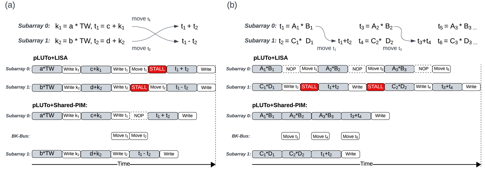
To demonstrate the advantage of using Shared-PIM in conjunction with an existing in-DRAM PIM design (pLUTo), we present two application-level use cases in Fig 4. We contrast our approach with the LISA architecture to highlight the specific improvements enabled by Shared-PIM.
Fig. 4(a) illustrates the mapping of the butterfly computation step in the Number Theoretic Transform (NTT) using two subarrays. In the figure, ‘a’ and ‘b’ represent the initial input data points, where ’a’ is processed in subarray 0 and ‘b’ in Subarray 1, with each being multiplied by the twiddle factor ‘TW’ to produce intermediate results for further computations. In the pLUTo + LISA configuration, a significant delay is observed because each subarray must wait until data transfer is complete before continuing with further computations, as marked by . While the Shared-PIM architecture also involves a wait for the BK-bus to complete before progressing with further computations due to data dependencies, this waiting time is not considered a stall because the subarray is available to be used for other computations during this period. This interval is labeled , standing for non-operation in the subarray. Despite the , the latency of the Shared-PIM for this butterfly computation is lower than that of LISA.
Fig 4(b) shows the mapping of a matrix multiplication segment using two subarrays. Here, ‘A1’, ‘A2’, ‘A3’, ‘B1’, ‘B2’, and ‘B3’ are the matrix elements handled by subarray 0, and ‘C1’, ‘C2’, ‘C3’, ‘D1’, ‘D2’ and ‘D3’ by subarray 1, with each pair being multiplied to contribute to the final matrix product. Subarray 0 is tasked with the operations , and Subarray 1 with . Once and are computed, the results and are immediately moved to the BK-bus, which is indicated by . This setup allows the subarrays to continue with subsequent operations like and without waiting for the data transfer, thereby overlapping data movement with computation. Furthermore, as does not depend on , in the pLUTo+Shared-PIM configuration, subarray 0 can immediate compute after . In contrast, in the pLUTo+LISA setup, both subarrays 0 and 1 are occupied with transferring so they cannot immediately perform any subsequent computation.
It is important to highlight that the data transfer time, denoted as in Fig 4, is shorter in Shared-PIM compared to LISA since LISA’s copy operation involves two separate steps as explained in Sec.III-A2. Moreover, Shared-PIM also consumes less energy during data transfers. The primary reason for these advantages is that Shared-PIM utilizes a direct link between subarrays, enabling data to be copied from the source row to the destination row in a single operation (see Sec II-B2). We compare our Shared-PIM approach with LISA in Sec. III-B.
IV Evaluation
In this section, we verify the functionality and assess the performance of Shared-PIM (integrated with pLUTo [3]) at both the circuit and application levels using DDR3 and DDR4 technology parameters, respectively. At the circuit-level, we compare Shared-PIM’s copy operation directly against RC-InterSA [11] as well as LISA [10]. At the application-level, we compare the pLUTo+Shared-PIM design with the pLUTO+LISA design [3].
IV-A Experimental Setup
Here, we explain the setup used to assess Shared-PIM’s functionality at the circuit-level, as well as to evaluate its performance at the application-level.
IV-A1 Circuit level
We implemented the Shared-PIM subarrays in SPICE using ASU’s low power 45nm predictive technology model (PTM) [12], with the JEDEC DDR3-1600 (11-11-11) timing parameters [13]. Note that this is the same setup used by LISA. Furthermore, we evaluated the latency and energy of Shared-PIM using the DDR3 DRAM configuration shown in Table I. We opted to include two shared rows per subarray so that one is always available for facilitating data transfers, while the other is utilized to store the computation result that will be transferred on the following cycle.
Our simulations confirmed that Shared-PIM can operate with the JEDEC DDR3-1600 (11-11-11) timing parameters, even with our modifications at the bank level (i.e., the addition of the BK-bus and BK-SAs), and the extra transistor in augmented DRAM cells. For energy evaluations, we employ the power models from Micron [21] and Rambus [16] to estimate the power consumption of the DRAM commands; these results were multiplied by the latency to quantify the energy dissipation of a copy operation using Shared-PIM. We estimate the Shared-PIM area based on the DRAM area breakdown reported in [3], along with added interconnect and transistor count overhead (the same method used in [3]).
| Model | Configuration | |||||
|---|---|---|---|---|---|---|
|
|
|||||
|
|
IV-A2 Application level
To evaluate the application-level performance of the pLUTo+LISA and the pLUTo+Shared-PIM designs, we employed the inter-subarray data transfer latency and energy results reported in [10], as well as our results from Shared-PIM, and combined them with the computational performance of pLUTo reported in [3]. Importantly, since [3] used the ASU’s low power 22nm PTM [12] and the DDR4 timing standards, we first employ SPICE simulations to test Shared-PIM using the DDR4-2400T (17-17-17) timing parameters used by [3].
Finally, the combined computational and data transfer performance of pLUTo+LISA and pLUTo+Shared-PIM were input into a Python-based, cycle-accurate simulator that provides a detailed cycle-by-cycle analysis of computation and subarray utilization. Notably, there is generally good agreement between our results and the results reported in [3]. Our method of evaluation, which employs (1) the cycle-accurate simulator, (2) the data transfer time of LISA, and (3) the operation latency (e.g., addition, multiplication, etc.) for end-to-end tasks (e.g., CNN inference) reported in pLUTo, is consistently within 15% of the performance reported in [3].
IV-B Circuit-level Functionality Validation

Fig. 5 depicts the waveforms from our SPICE simulations of Shared-PIM to simultaneously copy one source row to four destination rows in different subarrays over the BK-bus (i.e., a “broadcasting” operation). Once the source row is activated, the charge sharing stage between the cells and the BK-bus begins. At the beginning of the operation we observe the voltage of the source cell (blue line) declining, while the voltage on the BK-bus bitline (red line) rises as they share charge. Once the cell and the bitline reach equilibrium, the BK-SAs start sensing and amplifying the voltage on the bitline. We then activate the destination row(s) later, which causes the voltage drop at , while the voltage in destination cell (green line) rises. Similarly, after the charge sharing stage is finished, the BK-SAs begin amplifying the voltage on the bitline until the data is restored into the source and destination rows, which concludes the data transfer operation. Although four destination rows is not an absolute limit for the broadcast operation, and our simulations show that broadcasting to five or even six destination rows is possible, we keep the maximum number of destination rows to four to ensure it stays within the standard DDR timing limits.
IV-C Circuit-level Latency, Energy, and Area Evaluation

Table II reports the inter-subarray latency and energy for copying one row (8KB of data) from one subarray to another within the same bank using four different approaches: (1) memcpy, which uses the memory channel, (2) Rowclone (RC-InterSA), (3) LISA, and (4) our proposed Shared-PIM (with two shared rows per subarray).
With respect to inter-subarray copy latency, we further optimize Shared-PIM’s copy latency by overlapping the two ACTIVATE commands with only a 4ns delay between them as proposed in [8], resulting in a total copy latency of . Fig. 6 shows the command timeline and latency improvement of Shared-PIM with respect to RC-InterSA [11] and LISA [10].
The energy consumption reported in Table II was obtained with the method described in IV-A1, i.e., by calculating the power usage of the DRAM commands, and then multiplying this by the latency of a copy operation via Shared-PIM. Notably, the addition of two shared rows per subarray does not significantly affect the subarray’s energy, since it only adds two transistors per bitline (16K transistors per subarray, in total). Meanwhile, the addition of the BK-SAs that enable Shared-PIM’s data transfer raises the power consumption per copy operation. However, because the copy process is performed on the BK-bus with improved latency, the overall energy dissipation per copy operation is minimized compared to Rowclone [11] and the conventional memcpy. When comparing against LISA [10], it is apparent that Shared-PIM’s energy savings (1.2) are not as good as the latency improvements (5). This can be attributed to Shared-PIM’s additional BK-SAs, since the copy operation over the bus activates the entire bus which consists of four rows of sense amplifiers as explained in Sec. III, i.e., Shared-PIM’s copy operation activates four times the number of sense amplifiers that LISA does, which results in a trade off of power dissipation for latency improvements.
Finally, Table III shows the area breakdown of the base DRAM, the pLUTO architecture (using the BSA mode, which is pLUTo’s more compact implementation), and Shared-PIM (combined with pLUTo). We estimate a 7.16% overhead to pLUTO’s chip area with Shared-PIM, which is a result of the addition of BK-bus, BK-SAs, the GWL transistors (for shared cells), and GWL drivers. To further reduce the physical implementation complexity and the area overhead of Shared-PIM, the BK-bus lines could be implemented using a different metal layer than that of the regular bitlines.
| Copy Commands (8KB) | Latency (ns) | Energy (J) |
|---|---|---|
| memcpy (via mem. channel) | 1366.25 | 6.2 |
| RC-InterSA | 1363.75 | 4.33 |
| LISA | 260.5 | 0.17 |
| Shared-PIM | 52.75 | 0.14 |
| Area () | ||||||
|---|---|---|---|---|---|---|
| Component | BASE DRAM | pLUTo-BSA |
|
|||
| DRAM cell | 45.23 | 45.23 | 45.29 | |||
| Local WL driver | 12.45 | 12.45 | 12.45 | |||
| Match logic | - | 4.61 | 4.61 | |||
| Match lines | - | 0.02 | 0.02 | |||
| Sense amp | 11.40 | 18.23 | 18.23 | |||
| Row decoder | 0.16 | 0.47 | 0.47 | |||
| Column decoder | 0.01 | 0.01 | 0.01 | |||
| GWL driver | - | - | 0.05 | |||
| BK-bus lines | - | - | 0.04 | |||
| BK-SAs | - | - | 5.70 | |||
| Shared-PIM Row decoder | - | - | 0.01 | |||
| Other | 0.99 | 0.99 | 0.99 | |||
| Total | 70.24 |
|
|
|||
-
1
Shared-PIM’s overhead % is calculated with respect to pLUTo.
IV-D Application-level Evaluation


Here, we evaluate how data transfer in two architectures influences application-level performance. The architectures considered are pLUTo combined with LISA [3], and a scenario where pLUTo is integrated with our proposed Shared-PIM. We carry out our evaluation on two different fronts: (1) with operations of varied number of bits, and (2) by running five application benchmarks.
For varied number of bits, we study pLUTo’s performance for addition and multiplication operations. Given the size constraints of the LUTs in pLUTo, a single subarray cannot accommodate the entire LUT required for computations with higher number of bits. As a result, these computations are distributed across multiple subarrays. This distribution necessitates inter-subarray data transfers when executing a single operation, which can impact performance. In our experiments, we consider that a single pLUTo subarray can efficiently perform a 4-bit addition and 4-bit multiplication as reported in [3]. We then test pLUTo’s performance across varying bit-widths: 16, 32, 64 and 128 bits for both addition and multiplication. The inclusion of 128-bit operations demonstrates the advantages of using Shared-PIM in pLUTo for applications requiring high-precision computing and cryptography. Throughout these experiments, we assume that pLUTo executes these computations with maximum parallelism.
Fig. 7 compares the latency of pLUTo paired with LISA and pLUTo combined with Shared-PIM, for addition and multiplication, with varied number of bits. The benefits of Shared-PIM become increasingly apparent in computations involving operations with higher number of bits, as they require more data movement.
The speedup of Shared-PIM for addition operations can be attributed to its capability to execute all the 4-bit additions simultaneously. After these parallel operations, the results are forwarded to a subarray for final aggregation via the BK-bus. Shared-PIM enables efficient data transfer, allowing it to achieve a 40% performance improvement in 128-bit addition compared to LISA.
On the other hand, the scenario for multiplication is more challenging. Data dependencies in multiplication, especially for operations with higher number of bits, make it more challenging to achieve the same level of parallelism as in addition. This complexity stems from the combination of 4-bit multiplication, addition, and shifting. However, Shared-PIM offers significant advantages by enabling simultaneous computation and data transfer. For instance, while intermediate multiplication results are being transferred for final aggregation, Shared-PIM allows the next layer of multiplication and shifting operations to proceed immediately. Shared-PIM paired with pLUTo leads to a 40% improvement in performance for 128-bit multiplication compared to pLUTo combined with LISA.
For the study with application benchmarks, we explored the performance impact of our Shared-PIM design on pLUTo across five programs, which were selected for their varying levels of data dependencies. This selection allows us to compare and contrast the performance benefits of using the Shared-PIM architecture across different dependency scenarios. The benchmark programs are:
-
1.
Number Theoretic Transform (NTT): The NTT transforms polynomials into their modular equivalents in a finite field, functioning similarly to the Fast Fourier Transform (FFT). We evaluate the NTT using polynomial degree of 300.
-
2.
Breadth-First Search (BFS): The BFS application analyzes a 1000-node densely connected graph, where each node links to every other node, marking the highest amount of data dependencies among all of the selected programs.
-
3.
Depth-First Search (DFS): The DFS is similar to BFS, being a worst-case DFS that needs to visit each node and explore its neighbors.
-
4.
Polynomial Multiplication (PMM): Polynomial multiplication is the process of multiplying two polynomials to obtain their product. We use polynomials with a degree of 300. We employ a naive approach to polynomial multiplication (not using NTT to optimize).
-
5.
Matrix Multiplication (MM): Two matrices with a size of 200 200 multiply each other. MM has a high amount of data dependencies and requires significant data transfer between the elements of the matrices.
All the computations in these benchmark programs use 32-bit operations, and the latency and energy consumption are derived from previous tests for pLUTo with LISA and Shared-PIM architectures. We assume that both pLUTo with LISA and pLUTo with Shared-PIM can run these applications under full parallelism, which in this context means that an ideal number of computing arrays are available for these benchmark programs.
Fig. 8 presents the latency and energy consumption metrics for the benchmarks executed under pLUTo with LISA and the Shared-PIM architectures. The latency comparison reveals that Shared-PIM confers a substantial speed advantage in all tasks, with a 40% latency reduction in MM, 44% in PMM, and 31% in NTT. Shared-PIM enhances performance by enabling concurrent computation and data transfer within pLUTo subarrays, which facilitates the pipelining of data transfer with computation processes. Additionally, as shown in Fig.7, pairing Shared-PIM with pLUTo achieves an 18% speedup in 32-bit addition and a 31% speedup in 32-bit multiplication compared to the pLUTo with LISA setup, significantly boosting performance for individual operations.
The speedup for MM and PMM are particularly significant, as they are attributed to similar degrees of parallelism and computational steps. Compared to NTT, MM and PMM demonstrate greater speedup. This is primarily due to relative lower data dependencies in MM and PMM compared to NTT, allowing Shared-PIM to more effectively parallelize data transfer and computation in MM and PMM (as discussed in Sec. III-B). In our analysis, BFS and DFS show equal performance in worst-case scenarios on the same graph, as they follow identical processes.
With respect to energy consumption, a clear difference emerges despite the parallel capabilities of both designs. The Shared-PIM architecture proves to be more energy-efficient in data transfers than LISA, as indicated by the consistent reduction in energy usage. As a result, Shared-PIM achieves an average of 18% energy savings in data transfers across all benchmarks.
V Conclusion
This paper introduced Shared-PIM, a solution that strategically leverages shared rows and sense amplifiers in in-DRAM PIM banks for synchronized PIM operations. Shared-PIM demonstrates a remarkable reduction in copy latency and energy consumption – 5 and 1.2 lower than LISA [10], respectively. Additionally, it shows a notable improvement in basic computational tasks, with 1.4 faster addition and multiplication. These enhancements translate to substantial performance gains in real-world applications, as evidenced by the latency improvements of MM tasks by 40%, PMM by 44%, and NTT by 31%. Moreover, for graph processing tasks like BFS and DFS, Shared-PIM achieves a 29% improvement in speed with an area overhead of just 7.16% compared to a pLUTo baseline.
References
- [1] P. Siegl, R. Buchty, and M. Berekovic, “Data-centric computing frontiers: A survey on processing-in-memory,” in Proceedings of the Second International Symposium on Memory Systems, 2016, pp. 295–308.
- [2] O. Mutlu, S. Ghose, J. Gómez-Luna, and R. Ausavarungnirun, “Processing data where it makes sense: Enabling in-memory computation,” Microprocessors and Microsystems, vol. 67, pp. 28–41, 2019.
- [3] J. D. Ferreira, G. Falcao, J. Gómez-Luna, M. Alser, L. Orosa, M. Sadrosadati, J. S. Kim, G. F. Oliveira, T. Shahroodi, A. Nori et al., “pLUTo: Enabling massively parallel computation in DRAM via lookup tables,” in 2022 55th IEEE/ACM International Symposium on Microarchitecture (MICRO). IEEE, 2022, pp. 900–919.
- [4] H. Geng, J. Mo, D. Reis, J. Takeshita, T. Jung, B. Reagen, M. Niemier, and X. S. Hu, “PPIMCE: An In-memory Computing Fabric for Privacy Preserving Computing,” arXiv preprint arXiv:2308.02648, 2023.
- [5] D. Reis, H. Geng, M. Niemier, and X. S. Hu, “IMCRYPTO: An in-memory computing fabric for AES encryption and decryption,” IEEE Transactions on Very Large Scale Integration (VLSI) Systems, vol. 30, no. 5, pp. 553–565, 2022.
- [6] M. Li, H. Geng, M. Niemier, and X. S. Hu, “Accelerating Polynomial Modular Multiplication with Crossbar-Based Compute-in-Memory,” arXiv preprint arXiv:2307.14557, 2023.
- [7] K. Asifuzzaman, N. R. Miniskar, A. R. Young, F. Liu, and J. S. Vetter, “A survey on processing-in-memory techniques: Advances and challenges,” Memories-Materials, Devices, Circuits and Systems, vol. 4, p. 100022, 2023.
- [8] V. Seshadri, D. Lee, T. Mullins, H. Hassan, A. Boroumand, J. Kim, M. A. Kozuch, O. Mutlu, P. B. Gibbons, and T. C. Mowry, “Ambit: In-memory accelerator for bulk bitwise operations using commodity DRAM technology,” in Proceedings of the 50th Annual IEEE/ACM International Symposium on Microarchitecture, 2017, pp. 273–287.
- [9] S. Li, D. Niu, K. T. Malladi, H. Zheng, B. Brennan, and Y. Xie, “Drisa: A DRAM-based reconfigurable in-situ accelerator,” in Proceedings of the 50th Annual IEEE/ACM International Symposium on Microarchitecture, 2017, pp. 288–301.
- [10] K. K. Chang, P. J. Nair, D. Lee, S. Ghose, M. K. Qureshi, and O. Mutlu, “Low-cost inter-linked subarrays (LISA): Enabling fast inter-subarray data movement in DRAM,” in 2016 IEEE International Symposium on High Performance Computer Architecture (HPCA). IEEE, 2016, pp. 568–580.
- [11] V. Seshadri, Y. Kim, C. Fallin, D. Lee, R. Ausavarungnirun, G. Pekhimenko, Y. Luo, O. Mutlu, P. B. Gibbons, M. A. Kozuch et al., “RowClone: Fast and energy-efficient in-DRAM bulk data copy and initialization,” in Proceedings of the 46th Annual IEEE/ACM International Symposium on Microarchitecture, 2013, pp. 185–197.
- [12] W. Zhao and Y. Cao, “Predictive technology model for nano-CMOS design exploration,” ACM Journal on Emerging Technologies in Computing Systems (JETC), vol. 3, no. 1, pp. 1–es, 2007.
- [13] J. S. S. T. Association, “DDR3 SDRAM Standard JESD79–3F,” JEDEC Committee JC-42.3, Jul, 2012.
- [14] B. Keeth, R. J. Baker, B. Johnson, and F. Lin, DRAM circuit design: fundamental and high-speed topics. John Wiley & Sons, 2007, vol. 13.
- [15] Y. Kim, V. Seshadri, D. Lee, J. Liu, and O. Mutlu, “A case for exploiting subarray-level parallelism (SALP) in DRAM,” ACM SIGARCH Computer Architecture News, vol. 40, no. 3, pp. 368–379, 2012.
- [16] Rambus, “DRAM power model,” 2010.
- [17] Z. Al-Ars, M. Herzog, I. Schanstra, and A. J. van de Goor, “Influence of bit line twisting on the faulty behavior of drams,” in Records of the 2004 International Workshop on Memory Technology, Design and Testing, 2004. IEEE, 2004, pp. 32–37.
- [18] M. Redeker, B. F. Cockburn, and D. G. Elliott, “An investigation into crosstalk noise in DRAM structures,” in Proceedings of the 2002 IEEE International Workshop on Memory Technology, Design and Testing (MTDT2002). IEEE, 2002, pp. 123–129.
- [19] S. M. Seyedzadeh, D. Kline Jr, A. K. Jones, and R. Melhem, “Mitigating bitline crosstalk noise in DRAM memories,” in Proceedings of the International Symposium on Memory Systems, 2017, pp. 205–216.
- [20] T. Takahashi, T. Sekiguchi, R. Takemura, S. Narui, H. Fujisawa, S. Miyatake, M. Morino, K. Arai, S. Yamada, S. Shukuri et al., “A multigigabit dram technology with 6f/sup 2/open-bitline cell, distributed overdriven sensing, and stacked-flash fuse,” IEEE Journal of Solid-State Circuits, vol. 36, no. 11, pp. 1721–1727, 2001.
- [21] Micron, “DDR3 SDRAM System-Power Calculator,” 2011.