Shapiro steps in charge-density-wave states driven by ultrasound
Abstract
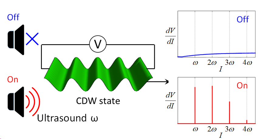
We show that ultrasound can induce the Shapiro steps (SS) in the charge-density-wave (CDW) state. When ultrasound with frequency and a dc voltage are applied, the SS occur at the current with integer . Even and odd multiples of SS are represented by two couplings between the CDW and ultrasound. Although an ac voltage bias with frequency induces the SS at , the ultrasound bias enhances the odd multiples more strongly than the even ones. This is the difference between the ultrasound and the ac voltage. Since the SS cause abrupt peaks in the , the extreme changes in the - curve will be applied to a very sensitive ultrasound detector.
The charge-density wave (CDW) is a macroscopic quantum state with twice the Fermi wave vector (2) induced by pairing of electrons and holes. The CDW is created by the electron-phonon interaction below the critical temperature of the Peierls transition , which opens a semiconducting gap at a Fermi surface (FS) and increases resistivity peierls55 . The CDW is pinned by impurities or in the case that a spatial period of the CDW matches with a lattice constant, i.e., commensurability pinning. When an applied electric field surpasses a certain threshold, the CDW is depinned and begins to slide through the lattice, increasing conductivity froelich54 ; allender74 ; lee74 ; fukuyama76 ; fukuyama78 ; lee79 . Remarkable transport properties were observed in transition metal trichalcogenides such as NbSe3 and TaS3 monceau76 ; takoshima80 ; monceau80 ; monceu85 ; gruner85 . A current generated by the sliding of CDW above the threshold dc field contains not only a dc but also oscillating components known as narrow-band noise fleming79 ; gruner81 ; monceau82 ; brown84 ; brown85 ; thorne86 . When a dc and an ac voltages are applied together, steps appear in an - curve fleming79 ; gruner81 ; monceau82 ; brown84 ; brown85 ; thorne86 . These steps are induced by phase locking of an external frequency with an internal one. This mechanism is same to the Shapiro steps (SS) in a Josephson junction of superconductors. The steps of an - curve in the CDW state shall be referred to as ”Shapiro steps”(SS).
Ultrasound has rich variety of applications. Ultrasonography is used in hospitals for biomedical diagnostics to view our bodies or to eradicate cancers. A touch sensor using ultrasound is installed in some monitors. The ultrasound attenuation technique was used to investigate the symmetry of superconducting order parameters tsuneto61 ; sigrist91 . On a surface of a ferromaget, a surface acoustic wave is used to control a spin current maekawa76 ; kobayashi17 ; xu20 . Recently, electrical control of a surface acoustic wave toward quantum information technology has been realized shao22 . In contrast to the electromagnetic waves, ultrasound does not radiate into free-space, allowing for coherent information processing and manipulation with a minimum cross-talk between devices and their environments maldovan13 . The ultrasound is generated and detected by a piezoelectric material such as lithium niobate. Improved ultrasonic sensitivity will broaden its use in quantum information technologies. Recently, the SS by mechanical vibration have been reported nikitin .
In this paper, we show that ultrasound can induce SS in the CDW state. When ultrasound with frequency and a dc voltage are applied, the SS occur at the current with integer . An ac voltage with frequency also induces the SS at . However, depending on the settings, the odd multiples of SS will be enhanced rather than the even ones due to two couplings of CDW to ultrasound; one contributes to even multiples, and the other to odd multiples. This is the difference between the ultrasound and the ac voltage. Since the shows sharp peaks due to the SS (See Fig. 1), the drastic changes in the - curve will be applied to a highly sensitive ultrasound detector.
The charge density in a CDW state is written by,
| (1) |
where averaged charge density and magnitude of -oscillation are constant. The dynamical behavior at low energies is given by,
| (2) |
where with Fermi velocity and is the velocity of Goldstone mode in the CDW state fukuyama76 . When dealing with one-dimensional electron systems, is related to fermionic operators of electrons using the bosonization given by, so as to with spin tomonaga50 ; luttinger63 ; solyom ; haldane81 . According to these equations, denotes the fluctuation of electron density around a FS. Considering with system size and number of electrons , corresponds to the electron density . Then, is associated with , because of the spatial derivative of the phase factors in leads to the electron density, i.e., tomonaga50 ; luttinger63 ; solyom ; haldane81 . The continuity equation defines the current .
The key to transport characteristics is CDW pinning. We shall now look at a single impurity model. An impurity potential at = 0 is given by,
| (3) | ||||
| (4) |
where , , 0 and 0. When ultrasound or surface acoustic wave is applied, the impurity is moved from its initial position and the energy provided by Eq. (6) is added,
| (5) | ||||
| (6) |
where nagaoka . At the impurity site, = , the spatial variation of is singular and its derivative is not continuous teranishi79 . The right (left) derivative of at the impurity site will be negative (positive) so as to fix the sign of . For , the pinning potential and the coupling to ultrasound are given by,
| (7) | ||||
| (8) | ||||
| (9) |
where = 1, and 0. In Eq. (9), the first term will be dominant in most circumstances because relates to as . It is usually less than 1, i.e., . Below, = 1 is imposed for brevity and the following results do not change qualitatively. The magnitude of the oscillation at the impurity site is proportional to , which can be regulated by the ultrasonic input power.
The single impurity model can account for several important aspects of CDW transport properties. This is the limit of strong pinning. When pinning is weak enough that a single impurity cannot pin the phase of the CDW, the pinning potential is determined by balancing the increase in kinetic energy owing to charge density change i.e., the second term of Eq. (2), and an energy gain from phase-dependent impurity pinning energy fukuyama78 ; lee79 . These are characterized by the pinning frequency in the optical conductivity fukuyama78 ; lee79 . The spatial distortions of the phase in the ground state caused by the random distribution of impurities are an important characteristic of impurity pinning. If the quantity of interest is not sensitive to such spatial fluctuation, the pinning will be characterized by an averaged potential proportional to , where is an averaged phase within an impurity distribution-determined domain fukuyama85 . Hence, the above discussion will be valid even in a weak pinning region.
Since electrons move together with lattice distortion, the effective mass of CDW is large and the dynamics of phase motion can be treated classically. Similar to the SS in a Josephson junction of superconductors, the transport properties of CDW can be calculated by,
| (10) |
with . Equation (10) is interpreted as the acceleration by the effective driving force, , with the friction term . In an overdamped region, , the first term in Eq. (10) is neglected. When ultrasound is used to drive a CDW, the transport properties are determined by,
| (11) |
where corresponds to a dc voltage. Below, we will use the following parametrization,
| (12) | ||||
| (13) |
The current is calculated by averaging of in time as,
| (14) |
Solving Eqs. (12) and (14), the - curves are obtained as shown in Fig. 2 with = 0.25, = 1.0 and = 1.0 (orange), 0.5 (blue), and 0.0 (red).
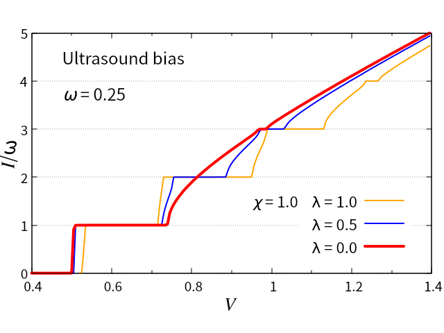
The SS appear at = for = 1.0 and 0.5. For = 0.0, however, the SS appear at only odd multiples, i.e., = 2+1, and even multiples are suppressed. This is a critical distinction between ultrasound and an ac voltage. When the system is driven by the ac voltage, the equation of motion is given by gruner81 ; monceau82 ,
| (15) |
Solving Eq. (15), the - curves are obtained as shown in Fig. 3 with = 0.25 and = 0.5 (red), 0.25 (blue), and 0.0 (black).
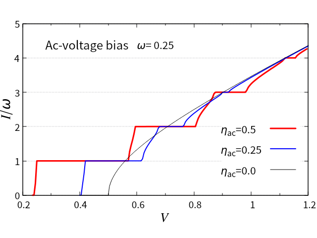
The SS appear at = similar to a Josephson junction of superconductors. In the case of Eq. (15), assuming with constants and , and using the relation, , with Bessel function , the potential term is transformed as, . When , the time average of is time-independent and leads to the SS. Since another potential term, such as , is multiplied by the oscillation in the ultrasound bias Eq. (13), analytical estimation of the SS is problematic. However, using the guess, , the potential term is written as, . Then, the SS appear at with even multiples. When =0, the oscillating term in Eq. (13) is proportional to . Hence, another guess of could be possible, and the SS appear at odd multiples as shown in Fig. 2.
The black line in Fig. 3 represents the threshold , at which the solution changes its behavior. At = 0, Eq. (15) is analytically solved as, . For , the solution is monotonously merging to a constant, whereas, for , the solution oscillatory increases or decreases with time. Considering Eq. (14), the increase or decrease of in time leads to a finite value of . Because of the phase-locking, the solution at the SS do not change its gradient.
In Fig. 2, without the -term in Eq. (9), the SS appear only at odd multiples. However, only with the -term, i.e., = 0.0, the - curves are presented in Fig. 4 for = 1.0 (green) and 0.5 (purple).
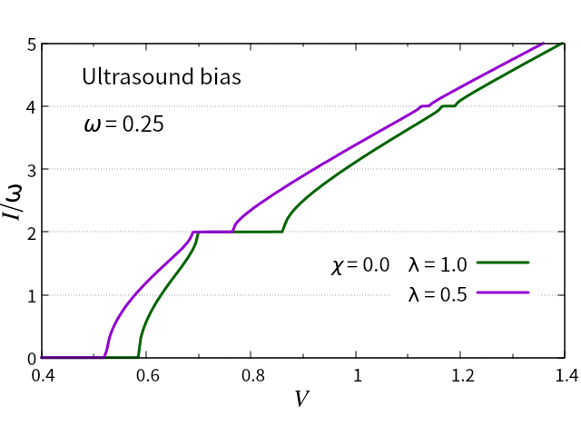
Notably, the SS appear at even multiples, i.e. = 2, which is in sharp contrast to Fig. 2. The -term in Eq. (9), , is not equivalent to due to . Hence, will be one of the possibilities of even multiples. Another reason is that the external force proportional to is nearly equivalent to the 2-oscillation.
We discovered that ultrasound can drive the CDW state in two ways, namely - and -terms in Eq. (9), which cause odd and even multiples in the SS, respectively. By definition =1 and , the odd multiples due to the -term will be dominant in the - curves. This will help to distinguish between an ultrasound contribution and an electromagnetic one. For example, the red curve in Fig. 2 is driven by 0.5 and another red curve in Fig. 3 is driven by 0.5. Just a factor of leads to completely different results. When ultrasound changes the dielectric constant of a material, an electromagnetic field would be simultaneously applied together with the ultrasound. In this case, the SS appear all of the integer multiples as = . The step-width at even multiples will be suppressed, if the produced electromagnetic field weakens. The electromagnetic bias is proportional to , while the ultrasound bias has an additional factor such as, and . Even though the difference is just a factor of , the step-widths are determined by their functional shapes. In the case of electromagnetic bias, all step-widths decrease with as shown in Fig. 3. There is not much of a distinction between even and odd multiples.
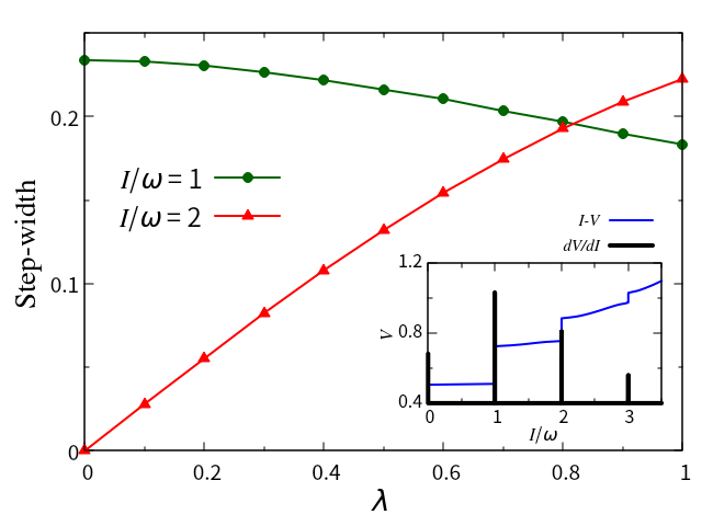
In Fig. 5, on the other hand, the step-width at =1 and 2 are plotted as a function of for =1.0. The step-width at =1 (green) drops modestly with , whereas the step-width at =2 (red) climbs fast from zero. Since is proportional to the density fluctuation, will be less than 1, i.e., , and hence the odd multiples such as =1 will be observed rather than even ones. The inset of Fig. 5 shows the - curve (blue) and its derivative (black) for = 0.5. The peaks corresponding to the SS in the - curve appear at = with integer . In this scenario, the is measured around a bias voltage, such as = 0.8. We will see the sharp peak in at = 1, only when ultrasound is applied. Furthermore, analogous to the Josephson junction of superconductors, this transition will be quite rapid and abrupt. As a result, the SS in the CDW state will detect ultrasounds with high sensitivity.
We have so far discussed the SS in the overdamped region. To test the effect of the kinetic term, i.e., the first term in Eq. (10), the - curve is calculated using the following equation,
| (16) |
The results are shown in Fig. 6 for =0.25, = 0.5, =1.0, and = 0.5 (red), 1.0 (blue), and 2.0 (green).
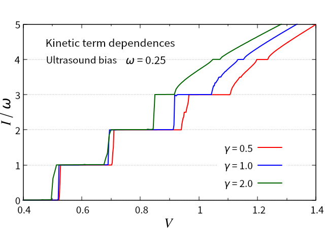
The SS arise independently of the kinetic term at = . As a result, even if the kinetic term exists, the SS in the CDW state will respond sensitively to the ultrasound. In the cases of =0.5 and 1.0, the - curves show tiny sub-harmonics at =2.5 and 3.5, respectively. The subharmonic steps ( = ) cannot be explained by the overdamped model with a single impurity, whereas the kinetic term changes the matching condition of the phase locking and can induce the subharmonic steps ya84 . Some materials exhibit subharmonic steps, the amount of which may be explained by factors other than the kinetic term brown84 ; brown85 . Another possibility to reproduce the subharmonic steps is multiple impurities in the overdamped model matsukawa87 ; matsukawa87jjap ; matsukawa87jpsj2 . In this situation, the subharmonic steps become evident in the same way that the harmonic steps do. Bardeen, on the other hand, proposed a non-sinusoidal potential in which an averaged impurity distribution is periodic and the CDW phase tunnels between two stable states thorne86 ; bardeen85 ; bardeen85book . The multiple impurities and the non-sinusoidal potential are outside our scope of this paper. Those will be studied in the near future.
We have shown that ultrasound can induce the SS in the CDW state. When ultrasound with frequency and a dc voltage are applied, the SS occur at the current with integer . Two couplings between the CDW and ultrasound constitute even and odd multiples of SS, respectively. Although an ac voltage with frequency induces the SS at , the ultrasound enhances the odd multiples more strongly than the even ones. This is the difference between the ultrasound and the ac voltage. Since the shows sharp peaks due to the SS (See Fig. 1), the drastic changes in the - curve will be applied to a highly sensitive detector of ultrasound.
Acknowledgements.
We would like to thank Prof Niimi and Mr. Fujiwara for valuable discussions about the experiments on SAW in 1D CDW materials. Thanks are also to Prof Matsukawa for his important suggestions and valuable discussions. This work was supported by JSPS Grant Nos. JP20K03810 and JP21H04987, and the inter-university cooperative research program (No. 202012-CNKXX-0008) of the Center of Neutron Science for Advanced Materials, Institute for Materials Research, Tohoku University. A part of the computations was performed on supercomputers at the Japan Atomic Energy Agency. S.M. is supported by JST CREST Grant (Nos. JPMJCR19J4, JPMJCR1874, and JPMJCR20C1) and JSPS KAKENHI (nos. 17H02927 and 20H01865) from MEXT, Japan.References
- (1) R. E. Peierls, ”Quantum Theory of Solids”, Oxford University Press, Oxford (1955).
- (2) H. Fröhlich, Proc. R. Soc. A 223, 296 (1954).
- (3) D. Allender, J. W. Bray, and J. Bardeen, Phys. Rev. B 9, 119 (1974).
- (4) P. A. Lee, T. M. Rice, and P. W. Anderson, Solid State Commun. 14, 703 (1974).
- (5) H. Fukuyama, J. Phys. Soc. Jpn. 41, 513 (1976).
- (6) H. Fukuyama and P. A. Lee, Phys. Rev. B 17, 535 (1978).
- (7) P. A. Lee and T. M. Rice, Phys. Rev. B 19, 3970 (1979).
- (8) P. Monceau, N. P. Ong, A. M. Portis, A. Meerschaut, and J. Rouxel, Phys. Rev. Lett. 37, 602 (1976).
- (9) T. Takoshima, M. Ido, K. Tsutsumi, T. Sambongi, S. Honma, K. Yamaya, and Y. Abe, Solid State Commu. 35, 911 (1980).
- (10) P. Monceau, J. Richard, and M. Renard, Phys. Rev. Lett. 45, 43 (1980).
- (11) ”Electronic Properties of Inorganic Quasi-One-Dimensional Materials I & II”, Ed. P. Monceau, D. Reidel Publishing Company, Dordreicht, Holland (1985).
- (12) G. Grüner and A. Zettl, Phys. Rep. 119, 117 (1985).
- (13) R. M. Fleming and C. C. Grimes, Phys. Rev. Lett. 42, 1423 (1979).
- (14) G. Grüner, A. Zawadowski, and P. M. Chaikin, Phys. Rev. Lett. 46, 511 (1981).
- (15) P. Monceau, J. Richard, and M. Renard, Phys. Rev. B 25, 931 (1982).
- (16) S. E. Brown, G. Mozurkewich, and G. Grüner, Phys. Rev. Lett. 52, 2277 (1984).
- (17) S. E. Brown, G. Mozurkewlch, and G. Grüner, Solid State Commu. 54, 23 (1985).
- (18) R. E. Thorne, J. R. Tucker, J. Bardeen, S. E. Brown, and G. Grüner, Phys. Rev. B 33, 7342 (1986).
- (19) T. Tsuneto, Phys. Rev. 121, 402 (1961).
- (20) M. Sigrist and K. Ueda, Rev. Mod. Phys. 63, 239 (1991).
- (21) S. Maekawa and M. Tachiki, AIP Conf. Proc. 29, 542 (1976).
- (22) D. Kobayashi, T. Yoshikawa, M. Matsuo, R. Iguchi, S. Maekawa, E. Saitoh, and Y. Nozaki, Phys. Rev. Lett. 119, (2017).
- (23) M. Xu, K. Yamamoto, J. Puebla, K. Baumgaertl, B. Rana, K. Miura, H. Takahashi, D. Grundler, S. Maekawa, and Y. Otani, Science Advances 6, eabb1724 (2020).
- (24) L. Shao, D. Zhu, M. Colangelo, D. Lee, N. Sinclair, Y. Hu, P. T. Rakich, K. Lai, K. K. Berggren, and M. Lončar, Nat. Electron. 5, 348 (2022).
- (25) M. Maldovan, Nature 503, 209 (2013).
- (26) M. V. Nikitin, S. G. Zybtsev, V. Ya. Pokrovskii, and B. A. Loginov, Appl. Phys. Lett. 118, 223105 (2021).
- (27) S. Tomonaga, Prog. Theor. Phys. 5, 544 (1950).
- (28) J. M. Luttinger, J. Math. Phys. 4, 1154 (1963).
- (29) J. Sólyom, Adv. Phys. 28, 201 (1979).
- (30) F. D. M. Haldane, J. Phys. C: Solid State Phys. 14, 2585 (1981).
- (31) Y. Nagaoka, Progress of Theoretical Physics 26, 589 (1961).
- (32) N. Teranishi and R. Kubo, J. Phys. Soc. Jpn. 47, 720 (1979).
- (33) H. Fukuyama and H. Takayama,”Electronic Properties of Inorganic Quasi-One-Dimensional Materials I”, pp. 41-104, Ed. P. Monceau, D. Reidel Publishing Company, Dordreicht, Holland (1985).
- (34) M. Ya. Azbel and P. Bak, Phys. Rev. B 30, 3722 (1984).
- (35) H. Matsukawa and H. Takayama, Synthetic Metals 19, 7 (1987).
- (36) H. Matsukawa and H. Takayama, Jpn. J. Appl. Phys. 26, 601 (1987).
- (37) H. Matsukawa, J. Phys. Soc. Jpn. 56, 1522 (1987).
- (38) J. Bardeen, Phys. Rev. Lett. 55, 1010 (1985).
- (39) J. Bardeen, ”Electronic Properties of Inorganic Quasi-One-Dimensional Materials I”, pp. 105-123, Ed. P. Monceau, D. Reidel Publishing Company, Dordreicht, Holland (1985).