Scaling theory of charge transport and thermoelectric response in disordered 2D electron systems: From weak to strong localization
Abstract
We develop a new theoretical scheme for charge transport and thermoelectric response in two-dimensional disordered systems exhibiting crossover from weak localization (WL) to strong localization (SL). The scheme is based on the scaling theory for Anderson localization combined with the Kubo–Luttinger theory. Key aspects of the scheme include introducing a unified function that seamlessly connects the WL and SL regimes, as well as describing the temperature () dependence of the conductance from high to low regions on the basis of the dephasing length. We found that the Seebeck coefficient, , behaves as in the WL limit and as () in the SL limit, both with possible logarithmic corrections. The scheme is applied to analyze experimental data for thin films of the p-type organic semiconductor poly[2,5-bis(3-alkylthiophen-2-yl)thieno(3,2-b)thiophene] (PBTTT).
pacs:
73.50.Lw, 73.20.Fz, 68.35.bmI Introduction
The development of high-performance thermoelectric (TE) materials is a focus of extensive research, particularly in relation to sustainable energy production. Since Hicks and Dresselhaus suggested in 1993 that a substantial increase in TE performance could be achieved by using low-dimensional semiconductors [1], numerous low-dimensional TE materials have been discovered. Recently, poly[2,5-bis(3-alkylthiophen-2-yl)thieno(3,2-b)thiophene] (PBTTT) thin films, composed of -stacked PBTTT polymers, have garnered significant attention as a new class of two-dimensional (2D) p-type organic semiconductors, both experimentally [2, 3, 4, 10, 11, 12, 9, 14, 15, 6, 5, 8, 7, 13] and theoretically [16, 17], due to their high TE performance. Because of the inherent structural disorder of polymers, understanding and controlling their charge transport and TE response pose important challenges in condensed matter physics and materials engineering.
Interesting experimental results on charge transport in p-type PBTTT thin film were reported by several groups [10, 12, 7, 13, 15]. Recently, Ito et al. measured the temperature () dependence of electrical conductivity, , for various hole densities controlled by an electrochemical transistor (ECT) [15]. They found that exhibits a logarithmic dependence, characteristic of weak localization (WL), in the range 200–100K. As decreases from 100 to 30K, deviates from this logarithmic behavior, which was attributed to a precursor to the crossover from WL to strong localization (SL), characterized by an exponential dependence of the conductivity. Similarly, experimental data on for similar hole density achieved by chemical doping have been reported by Watanabe et al. [9], who analyzed the data under the assumption of variable range hopping (VRH)-type exponential dependence.
In addition to electrical conductivity, the Seebeck coefficient, , has also been measured in a wide range by Ito et al. [15] and Watanabe et al. [9]. Despite the differences in carrier-doping methods, both groups conclude that is proportional to at high carrier densities, apparently consistent with the Mott formula for metals [18], whereas deviates from -linear behavior at low carrier densities. A coherent understanding of this behavior has not yet been achieved.
The purpose of the present study is to theoretically elucidate, on the basis of the scaling theory of Anderson localization, the dependence of and in the WL-SL crossover regime in 2D systems. This approach aims to provide a unified understanding of various experimental data obtained through different carrier-doping methods [15, 9], for which a consensus on the physical interpretation has not been attained.
II Theoretical scheme
II.1 Scaling theory at finite temperature
The scaling theory for the Anderson localization [19], i.e., Abraham–Anderson–Licciardello–Ramakrishnan (AALR) theory [20], indicates that the conductance in a disordered system at follows a differential equation:
| (1) |
where is the dimensionless conductance scaled by the universal conductance (: elementary charge, : Planck’s constant), is the length of the system, and is assumed to be a smoothly and monotonically increasing function with respect to .
In the large- limit, obeys the classical Ohm’s law as , where is conductivity and is the spatial dimension of the system. From Eq. (1), we see that the function in this limit is given by ; the asymptotic behavior of is therefore expressed as , where the expansion coefficient is a positive constant on the order of unity. On the other hand, in the small- limit, the electronic states are localized because of disorder and decreases exponentially with as , where is the localization length, resulting in in this limit. Thus, in the two limits, the function is given by
| (4) |
for -dimensional systems. In three-dimensional (3D) systems (), where conducting and localized states are sharply separated across the mobility edge, different theoretical schemes are needed for each state. By contrast, the 2D systems () of present interest exhibit in the limit of ; that is, the electronic states are always localized. If is finite and varied, is expected to crossover from metallic to insulating behaviors as is increased. Actually, this expectation has been confirmed through studies on the frequency () dependences of conductance for at by Vollhardt and Wolfle [21] and by Kawabata [22] using the self-consistent (SC) theory. Notably, the SC theory is governed by a single parameter, (where is the Fermi energy and is the elastic scattering time), which characterizes the scattering strength in quantum transport, and turns out to be capable of describing not only metallic but also insulating states. Regarding the dependence of conductance, however, we need to develop a different theoretical scheme. Once at finite temperatures, can be non zero even for and the dependence of exhibits a crossover from essentially metallic WL with to SL with exponential dependences. The characteristic temperature of this crossover depends on the carrier density.
To address the WL–SL crossover in 2D systems, we first consider and introduce the following function as a smoothly and monotonically increasing function that asymptotically behaves as in Eq. (4) in both limits of and :
| (5) |
To solve the differential equation in Eq. (1) with in Eq. (5), we impose as the boundary condition, where is the microscopic characteristic length that is much larger than the mean free path and is the conductance at length scale . Under this condition, Eq. (1) can be rewritten as
| (6) |
By solving Eq. (6) with Eq. (5), we obtain the dependence of at .
To extend this theory to finite , Anderson, Abrahams, and Ramakrishnan (AAR) proposed replacing the system length in Eq. (6) with a characteristic length (hereafter referred to as the dephasing length) over which an electron remains in an eigenstate [23] . In the diffusive transport in the WL regime, is given by with diffusion coefficient and dephasing time . Because the dephasing time generally depends on as with a positive constant , the -dependence of is given by . In the present work, we adopt as a single parameter to describe the dependences, similar to in at in the SC theory, and express it as
| (7) |
in terms of three different parameters: the temperature characterizing the WL-SL crossover and the dephasing length at and the exponent of the temperature dependence. This expression is possible because the dependence of conductance in a 2D system, unlike that in a 3D system with the mobility edge, exhibits a gradual change from logarithmic to exponential behavior in the dependences of the conductance as decreases.
In the WL limit, where is large and is satisfied, the differential equation in Eq. (6), with substituted for , can be solved analytically. The spectral conductance is given by
| (8) | |||||
with
| (9) |
resulting in the well-known logarithmic correction to conductance as long as . On the other hand, in the SL limit where is small (), the differential equation can also be analytically solved, enabling to be expressed as
| (10) |
for , where is defined as
| (11) |
II.2 Thermoelectric response in WL-SL crossover
The electrical conductivity and the Seebeck coefficient can be expressed in terms of as follows. In linear response theory, the electrical current density under the electric field and the temperature gradient can be described by . Here, the electrical conductivity and the thermoelectric conductivity can be expressed by the following Sommerfeld-Bethe (SB) relation based on the Kubo–Luttinger theory [24, 25] under the assumption that the heat current is carried only by electrons.
| (12) | |||||
| (13) |
where the factor of 2 accounts for the spin degree of freedom, and represent the length and cross-sectional area of the system, respectively, denotes the Fermi–Dirac distribution function, and is the chemical potential. Notably, the SB relation was originally derived from the Boltzmann transport theory (BTT); however, it is valid even for strongly disordered systems that cannot be treated by the BTT [26]. Using Eq. (12) and Eq. (13), we can describe the Seebeck coefficient by
| (14) |
Here, we note that the dependences of results from those of , , and in the present scheme. When the dependence of within is weak and can be approximated as linear with respect to , i.e., , the Seebeck coefficients in the two limits are respectively given as
| (15) |
and
| (16) | |||||
Here, , and , are respectively given by
| (17) | |||||
| (18) |
with , and
| (19) | |||||
| (20) |
Thus, is proportional to , whereas is proportional to and both of which have logarithmic corrections.
III Comparison with experiments
III.1 dependence of electrical conductivity
We here compare the present theory to the experimental data for PBTTT thin films obtained by two different carrier-doping methods: the electrochemical doping method [15] and the chemical doping method [9]. For the ECT fabricated by Ito et al. [15], the channel length between the source and drain electrodes is m, the channel width is mm, and the film thickness is nm. On the other hand, for the PBTTT device fabricated by Watanabe et al. [9], m, m, and nm. Note that the lamellar spacing of PBTTT (a distance between two layers in the PBTTT with a multi layered 2D structure) is nm; thus, the cross-sectional area of a single layer in Eqs. (12) and (13) is given by .
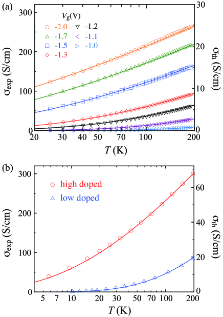
Figure 1(a) presents the experimental electrical conductivity, , under various gate voltages, , as measured using the ECT setup [15]. increases monotonically with increasing at a fixed , which is reasonable because the hole density increases. We also observe that is proportional to in the higher- region and deviates from this logarithmic behavior as decreases, which we ascribe to a precursor to the WL–SL crossover. The solid curves in Fig. 1(a) represent the dependences of theoretical results based on the assumption of nm, , and K, where is chosen as a typical temperature at which in Fig. 1 deviates from the logarithmic behavior. The three qualitatively different parameters (, , and ) obtained by fitting to experimental data are listed in TABLE 1, showing convincing agreement, except for the difference between the absolute values of and . We consider that the difference is due to uncontrolled sample conditions, such as layer numbers and types of spatial disorder.
Figure 1(b) shows the electrical conductivity of PBTTT thin films chemically doped at two different doping levels. The marks represent experimental data [9] and the solid curves are the present theoretical results based on the same assumption of nm, , K. The values of the three parameters (, and ) are listed in TABLE 2. The theoretical curves are in excellent agreement with the experimental data, except for the difference between their absolute values, similar to Fig. 1(a).
| 0.55 | 49.5 | 0.449 | |||||
| 0.88 | 54.0 | 0.437 | |||||
| 1.24 | 59.3 | 0.422 | |||||
| 1.51 | 64.4 | 0.410 | |||||
| 2.02 | 73.9 | 0.393 | |||||
| 2.31 | 77.3 | 0.392 | |||||
| 2.55 | 80.5 | 0.391 |
| Doping level | |||||||
|---|---|---|---|---|---|---|---|
| low | 0.92 | 42.7 | 0.441 | ||||
| high | 2.08 | 66.7 | 0.383 |
As changes from V to V, increases monotonically from to , which reflects the carrier density and the strength of disorder scattering, as characterized by parameter under the SC theory. This result suggests that, under these experimental conditions, the electrons in the PBTTT thin film are situated more or less in the WL regime rather than in the SL regime. The data in TABLE 1 also show that the dephasing length increases and the exponent decreases because of the delocalization of electrons with increasing . Similar tendencies in and are observed in the data in TABLE 2. Thus, the experimental data obtained by different carrier-doping methods can be understood in a unified manner using the three parameters , and .

As shown in TABLE 1 and TABLE 2, the exponent is which implies that is almost proportional to in the crossover regime where diffusive motions are assumed in the microscopic region. This dependence might indicate that Coulomb interaction is the dominant scattering processes in this regime [28, 29, 30]. It is of interest to see that the present result of based on quantum transport is close to that argued by Efros and Shklovskii [31], whose approach was based on the idea of VRH caused by electron–electron scattering. Such an interesting possibility of interaction effects in the crossover regime between conducting and localized regimes is a very particular property of 2D systems, in contrast to a sharp, though continuous, critical transition between them in 3D systems as analyzed recently for the Seebeck coefficient taking into account the energy dependences of the localization length near the mobility edge [33]. It is to be noted that in a 2D Mott VRH [32], where the electron hopping between localized states is caused by electron–phonon scattering.
III.2 dependence of Seebeck coefficient
We here discuss the dependence of data for PBTTT thin films obtained by the electrochemical doping method [15] and the chemical doping method [9]. Figure 2(a) shows the experimental of the PBTTT-based ECT under various [15]. The for all are proportional to in the high- region, where the electrical conductivity varies as , reflecting the WL. By fitting the experimental data using in Eq. (15), we determined and , as listed in TABLE 3, where can be obtained from Eq. (9). Both and increase as (or ) increases, as expected from Eqs. (9) and (17). In the low- region for low-doped cases of V and V, is expected to deviate from -linear behavior; however, corresponding experimental data are not available.
Figure 2(b) shows the for chemically carrier-doped PBTTT films [9]. In the case of high doping, is proportional to within a wide region from 30 to 200 K, reflecting the WL. By contrast, in the case of low doping, is also linear with respect to in the high- region but deviates from the -linear behavior in the low- region (the fitting parameters and for the high- and low-doped cases are summarized in TABLE 4). In the low- region, appears to vary as with . Notably, the -dependence of follows a power-law behavior, which is a characteristic feature of SL as shown in Eq. (16), even though the electrons in this low-doped PBTTT thin film are not in the fully SL regime but are somewhat more localized than in the WL regime.
| (mV/K) | (K) | (nV/K2) | ||||
|---|---|---|---|---|---|---|
| 215.8 | ||||||
| 161.9 | ||||||
| 121.0 | ||||||
| 102.3 | ||||||
| 78.3 | ||||||
| 65.6 | ||||||
| 54.5 |
| doping level | (mV/K) | (K) | (nV/K2) | |||
|---|---|---|---|---|---|---|
| low | 163.2 | |||||
| high | 84.1 |
IV Summary and outlook
We developed a new theoretical scheme for charge transport and TE response in disordered 2D electron systems. The proposed scheme can describe the WL–SL crossover on the basis of the AALR+AAR theory [23, 20] combined with the Kubo–Luttinger theory [24, 25]. The two key aspects of the scheme are (i) the introduction of the unified function, which seamlessly connects the WL and SL regimes, and (ii) the description of the dependence of the conductance from high and low regions in terms of in Eq. (7). Using this scheme, we predicted in WL and in SL, both with logarithmic corrections.
In addition, we applied this scheme to interpret recent experimental and data for PBTTT thin films, which are realized by two different carrier doping methods [15, 9]. As a result, we could provide a unified theoretical interpretation for both experimental data based on the new scheme. We found that the electrons in the PBTTT thin films used in both experiments [15, 9] are located more or less in the WL regime, not in the SL regime. We also found that in PBTTT thin films exhibits -linear behavior in the WL regime with a high carrier density but power-low behavior when the system begins to enter the SL regime from the WL regime as the carrier density decreases. Finally, we expect that the current theoretical scheme is applicable to other 2D materials (e.g., atomic layered materials) apart from present organic ones.
We thank Taishi Takenobu and Shun-ichiro Ito for fruitful discussions and for providing experimental data acquired using an ECT, We also thank Junichi Takeya and Shun Watanabe for valuable discussions regarding the experimental data obtained through the chemical doping method. This work was partly supported by JSPS KAKENHI (Grant Nos. 22K18954 and 23H00259).
References
- [1] L. D. Hicks and M. S. Dresselhaus, Phys. Rev. B 47, 12727 (1993).
- [2] S. Wang, M. Ha, M. Manno, C. D. Frisbie, and C. Leighton, Nat. Commun. 3, 1210 (2012).
- [3] D. Venkateshvaran, M. Nikolka, A. Sadhanala, et al., Nature 515, 384–388 (2014).
- [4] A. M. Glaudell, J. E. Cochran, S. N. Patel and M. L. Chabinyc, Adv. Energy Mater. 5, 1401072 (2015).
- [5] S. Zanettini, J. F. Dayen, C. Etrillard, N. Leclerc, and M. V. Kamalakar, Appl. Phys. Lett. 106, 063303 (2015).
- [6] K. Kang, S. Watanabe, K. Broch, A. Sepe, A. Brown, I. Nasrallah, M. Nikolka, Z Fei, M. Heeney, D. Matsumoto, K. Marumoto, H. Tanaka, S. Kuroda, and H. Sirringhaus, Nat. Mater, 15, 896-902 (2016).
- [7] S. D. Kang and G. J. Snyder, Nat. Mater. 16, 252 (2017).
- [8] Y. Yamashita, J. Tsurumi, M. Ohno, R, Fujimoto, S. Kumagai, T. Kurosawa, T. Okamoto, J. Takeya, and S. Watanabe, Nature. 572, 634–638 (2019).
- [9] S. Watanabe, M. Ohno, Y. Yamashita, T. Terashige, H. Okamoto, and J. Takeya, Phys. Rev. B 100, 241201(R) (2019).
- [10] H. Tanaka, K. Kanahashi, N.Takekoshi, H. Mada, H. Ito, Y. Shimoi, H. Ohta, and T. Takenobu, Sci. Adv. 6, eaay8065 (2020).
- [11] S. Fratini, M. Nikolka, A. Salleo, G. Schweicher, and H. Sirringhaus, Nat. Mater. 19, 491–502 (2020).
- [12] H. Ito, H. Mada, K. Watanabe, H. Tanaka, and T. Takenobu, Commun. Phys. 4, Article number: 8 (2021).
- [13] Y. Huang, D. H. L. The, I. E. Jacobs, X. Jiao, Q. He, M. Statz, X. Ren, X. Huang, I.McCulloch, M. Heeney, C. McNeill, and H. Sirringhaus, Appl. Phys. Lett. 119, 111903 (2021).
- [14] C. Chen, I. E. Jacobs, K. Kang, Y. Lin, C. Jellett, B. Kang, S. B. Lee, Y. Huang, M. B. Qarai, R. Ghosh, M. Statz, W. Wood, X. Ren, D. Tjhe, Y. Sun, X. She, Y. Hu, L. Jiang, F. C. Spano, I. McCulloch, and H. Sirringhaus, Adv. Energy Mater. 13, 2202797 (2023).
- [15] S-i. Ito and T. Takenobu (in preparation).
- [16] J.E. Northrup, Phys. Rev. B 76, 245202 (2007).
- [17] L.-H. Li, O. Y. Kontsevoi, S. H. Rhim, and A. J. Freeman, J. Chem. Phys. 138, 164503 (2013).
- [18] N.F. Mott and E.A. Davis,“Electronic Processes in Non-Crystalline Materials”, (Clarendon, Oxford, 1971), p. 47.
- [19] Anderson Localization, ed. Y. Nagaoka: Prog. Theor. Phys. Supplement 84 (1985).
- [20] E. Abrahams, P.W. Anderson, D.C. Licciardello and T.V. Ramakrishnam, Phys. Rev. Lett., 42, 673 (1979).
- [21] D. Vollhardt and P. Wölfle, Phys. Rev. B, 22, 4666 (1980).
- [22] A. Kawabata, Solid State Commun., 38, 823 (1981).
- [23] E. Abrahams, P.W. Anderson, and T.V. Ramakrishnam, Phys. Rev. Lett., 43, 718 (1979).
- [24] R. Kubo, J. Phys. Soc. Jpn. 12, 570 (1957).
- [25] J. M. Luttinger, Phys. Rev. 135, A1505 (1964).
- [26] M. Ogata and H. Fukuyama, J. Phys. Soc. Jpn. 88, 074703 (2019).
- [27] A.G. Zabrodskii and K. N. Zeninova, Eksp. Teor. Fiz. 86, 727 (1984).
- [28] E. Abrahams, P.W. Anderson, D.C. Licciardello and T.V. Ramakrishnam, Phys. Rev., 24, 6783 (1981).
- [29] H. Fukuyama and E. Abrahams, Phys. Rev. B 27, 5976 (1983).
- [30] H. Fukuyama, in A.L. Efros and M. Pollak (Eds.), “Electron-electron interactions in disordered systems” (North Holland, 1985), Chap. 5, p. 155.
- [31] A. L. Efros and B. I. Shklovskii, J. Phys. C8, L49 (1975).
- [32] N.F. Mott, J. Non-Cryst. Solids 1, 1 (1968).
- [33] T. Yamamoto, M. Ogata and H. Fukuyama: J. Phys. Soc. Jpn. 91, 044704 (2022).