Rough 1D Photonic Crystals: a transfer matrix approach
Abstract
Interfacial roughness is prevalent in 1D photonic crystals and other layered structures, but is not generally accounted for in their design nor the analysis of their optical properties due to a lack of simple theoretical approaches. We present a transfer matrix formalism to incorporate the effects of interfacial roughness in the optical properties of stratified systems such as 1D photonic crystals and apply it to calculate the optical response of some nanoporous anodic alumina and porous silicon structures. We have validated our formalism by comparing our results to some experiments.
Keywords: roughness, transfer matrix, photonic crystals, optical properties, porous alumina, porous silicon.
1 Introduction
Nanomaterials have gained a lot of interest in diverse fields of active research due to their unique properties. Manipulation of their composition, characteristic size, and shape allows tuning their optical, electrical and chemical properties, which might differ substantially from those of their components. In the last decades, the variety of synthesis procedures for nanomaterials has increased rapidly, and these structures can be found in several configurations [1] such as nanoparticles [2, 3, 4], aerogels [5], or thin films [6]. In particular, thin film nanomaterials have gained a lot of interest because they have the advantage of a simpler synthesis yielding a robust platform for design [7, 8, 9] that allows the fabrication of many nano-structures with diverse applications in optoelectronics [10], in solar cells [11], and even in portable nano-sensors using effects such as surface enhanced Raman scattering (SERS) [12]. Particularly interesting nano-systems are one-dimensional photonic crystals (1D-PhC), periodic multilayered systems that exhibit an optical band gap whose properties allow them to be used as a sensing platform [13, 14], such as an electromagnetic field assisted SERS sensor [15]. Diverse electromagnetic (EM) models have been implemented to understand the optical response of the thin films, and to obtain information from complex nanostructures embedded within the structure taking advantage of non-invasive and non-destructive techniques such as ultraviolet-visible (UV-Vis) spectroscopy [16, 17]. However, while many synthesis methods yield fluctuations of the geometric parameters of the nanostructures, the roughness of the interfaces has usually not been taken into account explicitly in the design or modeling of these nano-systems.
Roughness has been widely studied in regards to several optical phenomena[18] and at different wavelength scales. For one or two slab problems with up to three interfaces numerical methods have been used to solve Maxwell equations [19] and asymptotic models for coherent scattering have been applied [20]. These have been used in geophysical problems such as the study of reflections from geological layers of ground penetration radar signals. Nevertheless, these EM models are difficult to apply in multilayered problems. Roughness has also been considered in numerical simulations using finite differences in the time domain (FDTD) for 1D-PhC in the microwave region, and it has been shown to produce appreciable red shifts of high frequency features [21], a prediction that has been experimentally confirmed. There have been some efforts to model the coherent scattering for multilayered systems with rough interfaces in the microwave region employing the Kirchhoff approximation (KA) [22]. Infinite 1D-PhC’s composed of non-dispersive, non-dissipative media with rough interfaces have also been analyzed via 2D FDTD simulations [23]. For the case of wavelengths much larger than the period and for roughness heights not exceeding some small fraction of the period, their reflectance could be reproduced as well using an homogenization procedure [24]. Unfortunately these approaches do not take into account energy losses through scattering. Diffuse light scattering for surfaces with 1D roughness has also been studied [25]. There is a lot of work done on roughness effects on wave propagation [18, 26, 27], but many of these EM models are not easily carried to the case of 1D-PhC. Recently, a matrix formulation of the effects of roughness [28] has been developed for multilayered structures, but it cannot be easily incorporated into the convenient and well known transfer matrix method (TMM) [29] since it doesn’t yield unimodular matrices. In this work we present a TMM for stratified systems, such as 1D-PhC, that incorporates the roughness of the interfaces under the assumption of a small angle condition [30]. Under this condition, the scattering matrices [27] may be appropriately averaged to yield macroscopic interfacial transfer matrices that that can be combined with those of other films and interfaces to produce the full transfer matrix of the system, from which all of its optical properties can be obtained readily. These transfer matrices are consistent with the well known [26, 31] Kirchhoff approximation (KA), whose validity has been widely discussed [20, 22, 32, 33].
To test our formalism, we apply it to several systems and we compare its predictions to some experimental results. We first analyze the measured reflectance of a single nanoporous anodic alumina (NAA) film. We have selected NAA thin films due to their reproducibility [34] and versatile control through chemical means [35] for diverse applications [36]. By applying periodic current or voltage pulses during the anodizing process, NAA 1D-PhC may be obtained [13, 37]. Thus, we also study with our formalism their photonic band structure, their reflectance and transmittance, and we compare the effects of constant roughness to those of progressive roughness, dissipation, and thickness fluctuations. As NAA 1D-PhC structures have been reported to yield the best detection limits as sensor devices [36, 35], for quantifying optically the presence of analytes [38], we also analyze within our theory experimental NAA 1D-PhC data, expecting that incorporation of roughness considerations may lead to better sensor designs.
The structure of the paper is the following. In Sec. 2 we present our theory and we derive expressions for the transfer matrices of rough interfaces whose profile is uncorrelated to those of their neighbors interfaces, and we show how they can be incorporated into the usual transfer matrix of a multilayered system. In A we extend this theory to account for the possibility of several mutually correlated interfaces. In section 3 we apply our formalism to study the reflectance of a single rough slab and we make a detailed comparison between the sample parameters obtained directly from SEM and AFM images to those fitted from the optical reflectance using our model. In B we provide details of the preparation and characterization of our samples and of our optical measurements. In section 4 we study infinite and finite 1D-PhC’s, obtain their band structure and relate it to their reflectance. We compare the effects of roughness to those of absorption and of thickness’ fluctuations. We use these results in Sec. 5 where we measure and model the reflectance spectrum of a finite NAA 1D-PhC. Finally, Sec. 6 is devoted to our conclusion.
2 Theory
In this section we develop first the usual theory of transfer matrices for our stratified media with nominal flat interfaces in order to establish our notation. Then, we will show how to incorporate the roughness of the actual interfaces into the transfer matrix formalism under some simplifying assumptions.
2.1 Flat interfaces
We assume that the nominal system is time invariant and has translational symmetry along the plane, so that we can consider fields with a well defined frequency and 2D wavevector along . For local isotropic media and for a given TE or TM polarization, the transfer matrix is a 22 matrix that relates the components of the electric field and the magnetic field parallel to the plane, and normal to the axis of the structure which we take as the axis, evaluated at two arbitrary heights and ,
| (1) |
Several equivalent formulations have been proposed to obtain [39, 40, 41]. Within a homogeneous nonmagnetic layer characterized by a dielectric function and refractive index , the field is in general the sum of upward () and downward () going plane waves, with wavevector components along given by the dispersion relation
| (2) |
For economy in notation, we will use the nomenclature of plane waves even if is large, or is negative or complex, in which case, may acquire an imaginary part and the waves become evanescent. We define as the solution of (2) with a positive imaginary part. The surface impedance is defined as the quotient
| (3) |
From Faraday’s and Ampere-Maxwell’s equations we obtain
| (4) |
for upwards () and downwards () moving plane waves. It is convenient to write and in terms of the electric field amplitude of the waves for TE polarization and in terms of the magnetic field amplitudes for TM polarization. Denoting these amplitudes as in both cases, we write
| (5) |
and
| (6) |
where is the surface admittance. As propagate as plane waves for both polarizations, and
| (7) |
for any and within the homogeneous layer. Evaluating (5) and (6) at both nominal edges and of the layer of width (superscript denotes absence of roughness) and using (7) we obtain
| (8) |
for both TE and TM polarizations, where
| (9) |
is the transfer matrix of a homogeneous layer that transfers the fields across its nominal width . We remark that the determinant of this matrix is , as required to comply with time reversal symmetry.
The continuity of and imply that the fields may be transferred from the ambient towards the substrate through the layers by the matrix
| (10) |
2.2 Rough interfaces
We consider a system as above, but in which a single interface separating medium from is displaced from its nominal position at to a new position . The transfer matrix of the modified system can then be obtained by replacing and in (10) by and respectively. This is equivalent to the replacement of the product by , where we introduced an effective interface transfer matrix
| (11) |
Assuming now that all interfaces are shifted by a corresponding displacement , we can build the complete transfer matrix as the product
| (12) |
Now we introduce the roughness through and dependent height profiles , , as illustrated in figure 1.

In the spirit of the well known Kirchhoff approximation [26, 31] in the limit of low angle roughness [42] it seems tempting to apply (12) for each and average it over the plane, or, for a randomly rough system, over all realizations of an ensemble. For the case of mutually uncorrelated profiles, this would be equivalent to a replacement of by its average . Nevertheless, this would be wrong; the transfer matrix is not a quantity that may be meaningfully averaged, as the determinant of the average doesn’t agree in general with the average of the determinant, and the transfer matrix ought to be unimodular in order to be consistent with time inversion symmetry; even though , . Nevertheless, the scattering matrix of each interface is a quantity that may be safely and meaningfully averaged.
We define the scattering matrix for the -th interface as
| (13) |
as it produces the outgoing waves and when applied to the incoming waves and , namely,
| (14) |
where we defined the amplitudes and using the nominal plane as a reference, and where and are the reflection and transmission amplitudes corresponding to waves that impinge on the interface moving upwards () within layer or moving downwards () within layer . We may characterize the fields above and below the interface in terms of the components of through the matrices
| (15) |
and
| (16) |
for TE polarization, and
| (17) |
and
| (18) |
for TM polarization. These matrices yield the electromagnetic field extrapolated to each side, above and below the nominal surface when they act on the incoming amplitudes . Thus, we may relate and through and write
| (19) |
For a flat displaced interface we can obtain the elements of the scattering matrix either from Eqs. (11) and (19) or through a simple extrapolation of the fields from the actual towards the nominal interface,
| (20) |
where and are the Fresnel coefficients of the nominal interface [43] and . Thus, not unexpectedly, the effect of a rigid shift of an interface is to incorporate simple phase factors proportional to into the optical coefficients. The interfacial matrix (11) can be recovered in this case from Eqs. (15)-(20).
Going back to a rough interfacce, in the spirit of the Kirchhoff approximation for low angle surfaces [26, 27], we average (20),
| (21) |
we replace the optical coefficients by their averages in Eqs. (15)-(18) to obtain and and transferring the averaged fields across the nominal interface we obtain, in analogy with (19), the macroscopic interface transfer matrix as
| (22) |
From Eqs. (15), (16) and (21), we notice that for TE polarization
| (23) |
and
| (24) |
Nevertheless, from Fresnel’s formulae we obtain
| (25) |
so that and from (22) we verify the required unimodularity condition
| (26) |
It is trivially verified that this condition also holds for TM polarization.
Finally, we get a macroscopic unimodular transfer matrix for the complete system by replacing all the interface transfer matrices in (12) by their macroscopic counterparts (22),
| (27) |
We remark that although our formulation is close to that of [28], their matrix is not unimodular.
From the transfer matrix of the system we may obtain its optical properties straightforwardly using standard procedures. For example, the reflection and transmission amplitudes, and , when the system is illuminated from the ambient towards the substrate, may be obtained by solving the system of equations
| (28) |
and
| (29) |
Naturally, we define the nominal positions by demanding . Thus, in the limit of small height roughness we may approximate (21) to order by
| (30) |
where is the RMS height, so that all optical coefficients are reduced by a factor of order , with the free space wavelength. This wavelength-dependent reduction is due to the energy that is lost through scattering out of the specular direction and plays a role analogous but not identical to dissipation [44]. On the other hand, if is not necessarily small but obeys a Gaussian distribution with zero mean, we may evaluate (21) to obtain
| (31) |
A simple substitution of any of these into (22) yields the corresponding interface matrix . Thus, in the small roughness case (30) we obtain
| (32) |
and in the general case, we obtain
| (35) | ||||
| (38) |
For a Gaussian roughness we can further substitute (31).
In summary, we have developed a formalism that allows us to calculate the macroscopic effective transfer matrix of a multilayered system with rough interfaces using the Kirchhoff small-angle approximation. The transfer matrix is the product of the usual transfer matrices for each layer, corresponding to their nominal width, alternating with interface transfer matrices which can be obtained from the average of the corresponding scattering matrices. We obtained explicit expressions in terms of the variance of the height of the interface for the case of small height roughness and for the case of Gaussian roughness. In the following sections, we will illustrate the use of these matrices to calculate the optical properties of some rough stratified systems and we will compare some of our results to experiment. In A we extend the above theory to account for the possibility of several mutually correlated interfaces.
3 Application I: Nanoporous anodic alumina single rough film
In this section, we first test the proposed model on a single rough film of nanoporous anodic alumina (NAA) over an Al substrate. The sample preparation and the experimental procedures are described in detail in B. We measured with an atomic force microscope (AFM) the surface profile , its RMS mean , the profile slope and its RMS mean , averaging over several positions on each sample. All studied samples exhibited , so that the small angle approximation holds, giving us confidence in the use of the Kirchhoff approximation.
Table 1 summarizes the preparation and properties of 3 samples: an electropolished Al surface (S1), as those used as substrates for S2 and S3 which correspond to NAA films grown under different anodizing conditions.
| Sample | Anodization | Characterization | Fit | |||||||
|---|---|---|---|---|---|---|---|---|---|---|
| [s] | Electrolyte | [nm] | [nm] | [%] | [nm] | [nm] | [%] | |||
| S1 | 300 | 10 | HClO4 | 2 | - | - | 1.5 | - | - | |
| S2 | 30 | 11.2 | H2SO4 | 5 | 260 | 15 | 5.8 | 278 | 20 | |
| S3 | 30 | 44.8 | H2SO4 | 6 | 1020 | 30 | 5.1 | 1130 | 30 | |
The samples were characterized using a scanning electron microscope (SEM) to measure their thickness and porosity and an atomic force microscope (AFM) to determine their roughness. The uncertainties are around 10-15% for parameters defined by the SEM and AFM measurements.
As an example, in figure 2 we show some of the analyzed images for the sample S2, including top- and side-view SEM micro-graphs and an AFM height map.
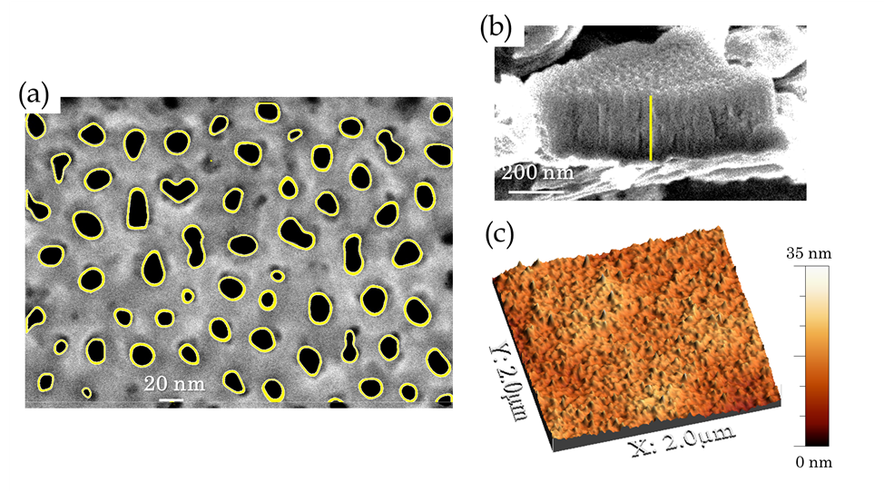
We developed a computational code in the PERL/PDL language [45] to identify and measure the pores from our SEM images and draw their porosity maps. In figure 2a we superposed the porosity map on the SEM top view image. We obtained the thickness from the side view (figure 2b) using the ImageJ package [46]. Notice that our sample has texture on two scales, as can be observed in the AFM image (figure 2c). The smallest one corresponds to the pores, and we deal with it by homogenizing it using an effective medium theory [47]. The remaining texture is dealt through our transfer matrix model for rough layers.
We measured the reflectance as described in B for the 3 samples described in Table 1. We fitted the results using (27) and the Gaussian roughness model. We obtained the reflection amplitude and the reflectance from Eqs. (28) and (29). As an example of our fitting procedure, in figure 3 we show the normal-incidence reflectance

measurement for sample S2 as a function of frequency and wavelength and the corresponding fits under different assumptions. To perform any of the calculations we need the refractive index for all the relevant media. The substrate is Al [48] while the film is NAA. The refractive index of the alumina phase was taken from reference [49], but to account for the nanoporous character of the film we took the porosity as an adjustable parameter and we applied Bruggeman’s 2D [47] effective media theory to obtain the index of the film. This is a very simple model but is satisfactory enough for the system under study. The fitting parameters were the RMS heights of both interfaces (which we assumed to be equal), the thickness and the porosity . We obtained these three parameters using the MINUIT optimization package [50]. Figure 3 shows that in the absence of roughness the calculated reflectance displays interference oscillations with a separation that is simply related to the nominal optical thickness of the film. Our experimental results display these oscillations, but they also show a decrease in the value of the reflectance as the frequency increases. This decay is also displayed by the fitted curve that incorporates roughness, yielding a fitted roughness of nm. If we also account for dissipation within the alumina, due to the presence of impurities of and CuO with concentrations and respectively, as corresponds to Al 1100 [51] we obtain slightly smaller fitted roughness nm.
These results may be qualitatively understood through the wavelength dependent scattering out of the specular direction that is incorporated implicitly within our model. As discussed above (30), this effect is of order .
The agreement between theory and experiment for the other samples is similar to that shown in figure 3 for sample S2. All the fitted parameters are also included in Table 1 and for the NAA slabs correspond to the dissipative case. Notice the good agreement between the fitted parameters and the corresponding parameters obtained from AFM and SEM. For the case of the fitted parameters, the uncertainty is around taking into account experimental data from different sample scanned regions.
4 One Dimensional Photonic Crystal
We consider a 1D photonic crystal (1D PhC) consisting of the periodic alternation of two layers of refractive indices and , nominal thicknesses and and period . We assume their interfaces are rough, described by small mutually uncorrelated height functions with corresponding RMS values and . Our formulation above allows us to incorporate the effects of roughness into an effective macroscopic transfer matrix for one period by simple matrix multiplication of the appropriate interface matrices, such as
| (39) |
The normal modes of the system are Bloch waves which are easily obtained from the transfer matrix by solving the eigenvalue problem
| (40) |
to obtain the eigenvalues
| (41) |
and eigenvectors
| (42) |
where is the Bloch vector along the axis of the structure and are the surface impedances for Bloch waves propagating (or decaying) towards evaluated at the position , corresponding to the even numbered interfaces. As the transfer matrix is unimodular, we can rewrite the dispersion relation as
| (43) |
where , are the matrix elements of . The impedances are
| (44) |
4.1 Photonic Bands
In figure 4 we show the dispersion relation vs. of the Bloch waves of an infinite 1D-PhC, calculated as discussed above for parallel wavevector .

The system consists of two alternating films with thicknesses =100nm and =80nm. To elucidate the role of roughness and of dissipation, we calculated the modes for three cases: dispersionless, dissipationless media with flat surfaces (, , ), the same system with some dissipation artificially added (, , ), and the same system without dissipation but with some Gaussian roughness (, , nm, nm). For the dissipative case we added an imaginary part to equal to 10% of its real part. For the rough case, we chose the roughness amplitude as 10% of the width of the corresponding layer. Notice that this roughness is not small for the highest frequencies in the figure. Thus, (32) is not applicable, but we use (35). For the flat system without dissipation (figure 4, left) we found, as expected, bands for which the modes may propagate, with and with alternating positive and negative group velocity, and gaps for which propagation is forbidden and the modes decay exponentially, with and or , at the center or at the edges of the Brillouin zone. The center of the gaps are at frequencies whose corresponding free-space wavelength is a sub-multiple of twice the optical width of a period, yielding constructive interference of the waves back-scattered by successive periods,
| (45) |
and where peaks. In the case with dissipation (figure 4, center), also displays maxima corresponding to the gaps, but for those frequencies is no longer a constant at the center or at the edges of the Brillouin zone, corresponding to both decay and propagation. There are also regions where becomes relatively small, corresponding to the propagating bands, but it is not zero, so there is some decay due to extinction through absorption. For high enough frequencies the minima of is almost , so that the decay distance becomes of the order of one period. Of course, these are not actual modes that may be excited within an infinite system, but they may be excited in truncated photonic crystals or in crystals with defects. In the case with roughness (figure 4, right), the results are very similar to those obtained in the case with dissipation, as roughness also yields extinction, though its origin is scattering out of the specular direction instead of absorption. We remark that we didn’t calculate explicitly the non-specular scattered fields, but the optical theorem implies that the energy they carry away manifests itself through destructive interference in the specular term [29].

In order to explore roughness effects for realistic systems, in figure 5 we show the band structure for a nanoporous anodic silicon (NAS) 1D-PhC made of two alternating layers with porosities % and % and widths nm and nm, as obtained from [52]. We obtained from the porosity and the dielectric function of silicon, taken from Palik’s handbook [48], using the Bruggeman 2D model [47]. In figure 5 we show results corresponding to a flat structure and to a structure with rough surfaces considering two cases, a RMS height of 10% of the corresponding layer’s width, i.e., nm and nm, and a RMS height of 20% of the layer’s width ( nm and nm). As expected, the middle of the first band gap at eV complies with (45), with . For this system, the effects of dissipation dominate those of roughness. For the 10% case the roughness corrections are barely visible, though for the 20% they are relatively small but clearly discernible. We expect roughness to be more important for materials with a smaller dissipation, such as NAA.

In figure 6 we show the band diagram of an NAA 1D-PhC made up two alternating layers of widths nm and nm and porosities and . We used Bruggeman’s 2D model in order to calculate the dielectric functions () of the porous layers from that of Al [51, 48]. The calculation was done both for the case of flat interfaces but including dissipation within the alumina due to impurities of and CuO, as in Sec. 3, and for that of rough interfaces characterized by nm and nm (so that ) and without dissipation within the alumina. We plot the imaginary part of the Bloch vector . Two band gaps are clearly seen in the band structure, consistent with (45), in which the imaginary part of Bloch’s vector has large peaks (see inset of figure 6) with or without roughness of the order of , corresponding to small penetration depths of . Besides the gaps, there are propagation bands for which would be null in the absence of roughness or dissipation. Nevertheless, for the rough system and takes values as high as corresponding to a penetration distance of at most periods. For the parameters chosen, the effects of roughness are qualitatively similar to those of dissipation.
4.2 Finite 1D-PhC
Now, we consider a finite stratified system of width made from repetitions of a unit cell composed of two layers of nominal thicknesses and , refractive indices and , and with mutually uncorrelated rough surfaces characterized by the RMS heights and , respectively. The refractive index of ambient is while for the substrate is . We can obtain the reflectance and transmittance of the system from Eqs. (27)-(29).


In figure 7 we show the normal incidence reflectance and transmittance spectra of a free standing finite 1D-PhC in air () consisting of periods of the same photonic crystals as in figure 4, with and without dissipation and roughness. We also present results for a system with flat surfaces and no roughness nor dissipation, but whose thicknesses have mutually uncorrelated fluctuations, and for a system without dissipation nor width fluctuations but with a roughness whose amplitudes grow linearly from the surface towards the substrate. As shown in the top row of figure 7, in the case without dissipation, roughness nor fluctuations, there are relatively wide regions of very high reflectance and very small transmittance corresponding to the band gaps shown in figure 4. Outside of these regions, the reflectance and transmittance show strong oscillations due to the interference of the waves reflected from the front and back surfaces of the system. These oscillations take to values as low as 0. Correspondingly, takes values as high as 1.
In the second row of figure 7, we show the reflectance and transmittance averaged over an ensemble of 1D-PhC’s as those corresponding to the first row, but with fluctuations in the widths of each film obeying a Gaussian distribution with standard deviations nm and nm corresponding to of their nominal widths. We used one thousand ensemble members for our calculation. The purpose of this calculation is to allow for a finite transverse coherence length [29] for the incident light, so that the contributions to the reflectance and transmittance from illuminated regions farther apart than add incoherently. This situation will prove relevant for the system studied in the next section.
The results show regions where and as in the top row, but the oscillating structure due to the interference is damped by the averaging process, as the frequencies corresponding to each maxima and minima differ for each member of the ensemble. This damping is larger at higher frequencies, for which the oscillations displayed by the first row become narrower and their frequency spacing becomes smaller. The third row of figure 7 shows the effects of roughness characterized by the amplitudes nm. In this case, shows maxima corresponding to the band gaps of figure 4, but they don’t attain the value 1, as in the top and second rows. The reason is that in this case, energy is lost through scattering, reducing the specular reflectance. In our treatment of roughness, we averaged scattering matrices, thus incorporating phase information that is not present in our treatment of thickness fluctuations corresponding to the second row of figure 7, for which we averaged the reflectance and transmittance. Hence the qualitative differences. Corresponding to the maxima in for the case of a rough surface there are minima in . Nevertheless, most of the energy is reflected or scattered away so that beyond the transmittance becomes negligible. The third row of figure 7 also shows results for a flat absorptive system with and . The result of dissipation is similar to that of roughness without dissipation.
In the bottom row of figure 7 we show the effect of a roughness that increases linearly in height from the front () towards the back (nm) so that its average coincides with that considered in the third row. In this case, the reflectance does attain the value corresponding to the band gaps, as in the first row, since within the gaps most of the electromagnetic energy is reflected before reaching the deep layers and thus it doesn’t sense the larger roughness. Nevertheless, the interference oscillations of the first row corresponding to the propagating bands are smoothed out as in the second and third rows. On the other hand, the transmittance is very similar to that of the third row for all frequencies as the transmitted energy is scattered away by the rough deep layers. If we invert the roughness progression, the results would be similar to those in the third row.
In the next section we will explore a real stratified system for which the analysis of roughness that increases with depth plays a relevant role.
5 Application II: NAA 1D-PhC
We prepared an NAA 1D-PhC made of 60 repetitions of two alternating NAA layers of different porosities and widths on an Al substrate by following the procedure described in B. We used Bruggeman’s 2D model [47] to calculate the dielectric response of the porous alumina layers in terms of their porosity and the alumina response. We designed the system so as to have a resonance (45) at the mid UV-Vis range.
In figure 8 we show the normal incidence reflectance spectrum obtained experimentally together with several fitted theoretical curves. We considered models with flat interfaces, with constant roughness and with linearly increasing roughness, incorporating in all cases thickness fluctuations.

All of the fitted spectra reproduce the reflectance maximum around 2.4eV. In the absence of roughness the curve flattens out for higher energies. Roughness yields a decrease of for frequencies above the peak due to the extinction of the specular fields as a consequence of scattering, but the high frequency fit is much better for the case of progressive roughness. Such parameter optimization was performed using the MINUIT package. The fitted parameters are the porosities (, ), the nominal thicknesses (nm, nm), the Gaussian fluctuations of the layer widths (nm), and the roughness height (nm for a constant roughness and nmnm for linearly increasing progressive roughness). Since the current densities used for the 1D-PhC are those of S2 and S3, the fitted porosities and are similar to those reported in Table 1 and the fitted thicknesses were in accordance to the expected ones, given the growth conditions used. The roughness heights are higher than for the single slabs of Sec. 3 which suggests that there exists an accumulation effect on the roughness when the unit cell is repeated several times.
6 Conclusions
We have developed a transfer matrix formalism for stratified systems such as 1D photonic crystals that is capable of incorporating in a very simple way some effects of the interface roughness. We assumed the rough surface obeys the small angle condition. Under this approximation [30] the scattering matrix [27] of each interface acquires a local phase that may be averaged to produce macroscopic interfacial transfer matrices (22) whose determinant is 1, and that may be incorporated into the transfer matrix of the whole system. The interfacial matrices are consistent with the well known [26, 31] Kirchhoff approximation (KA), whose validity has been amply discussed [32, 20, 22, 33]. From the total macroscopic transfer matrix all optical properties follow through the usual procedures for layered systems. We extended the formalism in an appendix to the case where nearby interfaces have mutually correlated roughness.
We employed our formalism to study a single NAA film on an Al substrate. We verified that our assumptions held for our samples through AFM and SEM characterizations. We observed the characteristic oscillations due to interference between the fields reflected by both interfaces of the film. Roughness yields a decrease in the reflectance for increasing frequency due to the extinction of the specular fields through increased scattering. This decrease is observed experimentally and is absent from the results for flat films. Furthermore, we found a good agreement between the parameters of the system fitted to our measurements of the reflectance and the corresponding parameters measured directly through SEM and AFM microscopy.
We also analyzed theoretically the photonic band structure of infinite periodic multilayered systems. We found that roughness has an effect similar to that of dissipation. Both blur the distinction between propagating bands and band-gaps and produce a finite decay length within the system, as extinction can be produced by scattering as well as by absorption. When both absorption and roughness are present, their effects compete and one or the other may dominate.
We studied finite slices of photonic crystals and compared the effects of roughness to dissipation and to fluctuations in the film widths. We found that roughness, dissipation and fluctuations in the widths eliminate the oscillations due to the interference between multiple reflections from the boundaries. Furthermore, roughness and dissipation produce a similar decrease in the reflectance maxima at the band-gaps, but width fluctuations do not. We also studied progressive roughness that increases towards the substrate, and which is expected in systems such as NAA prepared by an electrochemical attack from the front towards the back.
Finally, we applied our formalism to model the reflectance of an NAA photonic crystal on an Al substrate and compared experimental and theoretical results. Experiment and the theory show a maximum due to constructive interference of fields reflected by successive periods, but there is a decrease of the reflectance for higher frequencies which is well reproduced by the model that incorporates roughness but not by the model with flat surfaces.
In summary, we developed a very simple theory which allows us to incorporate roughness into standard transfer matrix calculations of the optical properties of stratified media. We calculated properties of single films, of finite Bragg mirrors and of infinite superlattices, and compared results to experiment. Our results show that structural parameters that may be difficult to measure directly may be obtained by analyzing optical properties and using our formalism. Thus, we conclude that when applicable, our formalism is useful and convenient.
Acknowledgments
LLM is grateful to CONICET for its support through a scholarship. MLMR is member of CONICET and acknowledges grants UBACyT 20020170200298BA and PIO 33APIO007. GPO acknowledges the support of ANPCyT-FONCyT through grant PICT-0696-2013 and SGCyT-UNNE trough grants PI-F008-2014 and PI-18F008. WLM acknowledges the support of DGAPA-UNAM through grant IN111119.
Appendix A Correlated rough interfaces
We extend the formalism of Sec. 2 to account for correlations between two or more interfaces, as illustrated in figure 9.

In case the interfaces are correlated, we consider the corresponding contributions to the displaced transfer matrix (12)
| (46) |
we obtain its corresponding scattering matrix relating the outgoing amplitudes and to the incoming amplitudes and by solving Eqs. analogous to Eqs. (28) and (29), use them to construct the left and right matrices and , average them, and use them to construct a macroscopic slab transfer matrix
| (47) |
which may be spliced into (27) replacing the product to obtain the macroscopic transfer matrix
| (48) | ||||
of the rough correlated system.
Appendix B Experimental Section
B.1 Materials
Square plates of 20mm side were obtained from commercial 0.8mm thick Al 1100 [51] sheets. Sulfuric (H2SO4) and perchloric acid (HClO4) (Sigma-Aldrich) were used without further purification. Biopack absolute ethanol and ultra-pure water were used to prepare solutions. Sintorgan pure Acetone, Biopack Sodium hidroxide (NaOH), and Cicarelli Nitric acid (HNO3) 65% were used for cleaning.
B.2 NAA Sample preparation: Thin Films and 1D-PhCs
Prior to the anodizing process, Al foils were cleaned by sequentially immersing and draining them in acetone for 5 min, in 10%m/v sodium hydroxide solution for 1 min, and nitric acid 50%v for 1 min. Afterwords, they were thoroughly rinsed in bi-distilled water.
All samples were electroplated by setting them on a stainless steel cathode with a contacting surface larger than the sample surface and applying a potential of 10-12 V while immersed in a 1:4 solution of perchloric acid and absolute ethanol. As electroplating is an exothermic reaction, it was performed in a thermal bath with ice. The best electroplated Al samples, with reflectance larger than 80% and without significant dispersion in the optical spectral range, were obtained by fixing the voltage at 10 V during 5 min. To prepare NAA samples we applied a registered procedure [37] with an electrolyte composed of a solution of sulfuric acid 15%m/v and used a home-made voltage and current PC controlled sources to operate the anodizing cell [53]. We have synthesized samples of NAA films and 1D-PhC’s on the Al samples. NAA thin films were prepared at different current densities and for different times as specified in Table 1 in the manuscript. NAA 1D-PhC’s were prepared by first growing a protective thick film at 15V during 600s and then by producing two alternating NAA layers at =44.8mA/cm2 for =4.5s and =11.2mA/cm2 for =22s. This binary unit was repeated 60 times. Following the anodizing procedure [37] to produce for each several NAA films samples and by applying a linear regression of its thickness versus anodizing times we have obtained the linear growth rates nm/s and nm/s.
B.3 Characterization Techniques
We used an Ocean Optics USB-4000 spectrometer to measure the intensity of our deuterium-tungsten-halogen light source (DT-MINI-2 Ocean Optics), the intensity reflected at normal incidence from the NAA films and the reference intensity reflected from an Al film evaporated onto a glass substrate. We adapted a reflection probe to the spectrometer above to characterize UV-Vis-NIR optical properties. Scanning Electron Microscopy (SEM) images were obtained for single NAA films using a Zeiss Ultra 55 microscope. Front views and cross-section were performed to measure porosity and thickness respectively. Multi-mode 8 Atomic Force Microscopy (Nanoscope V controller, Bruker, Santa Barbara) was used in contact mode to get the NAA profiles. The cantilever spring constant was 0.32 N/m.
References
References
- [1] Song-Yuan Ding, En-Ming You, Zhong-Qun Tian, and Martin Moskovits. Electromagnetic theories of surface-enhanced Raman spectroscopy. Chem. Soc. Rev., 46:4042–4076, 2017.
- [2] T.S.Ahmadi, Z.L. Wang, T.C. Green, A.Henglein, and M.A.El-Sayed. Shape-controlled synthesis of colloidal platinum nanoparticles. Science, 272:1924, 1996.
- [3] V.F.Puntes, K.M.Krishnan, and A.P.Alivisatos. Colloidal nanocrystal shape and size control: the case of cobalt. Science, 291:2115, 2001.
- [4] G.Rodriguez-Gattorno, D.Díaz, L.Rendón, and G.O. Hernández-Segura. Metallic nanoparticles from spontaneous reduction of silver(i) in dmso. interaction between nitric oxide and silver nanoparticles. J. Phys. Chem. B., 106:2482, 2002.
- [5] M.L. Anderson, C.A. Morris, R.M.Stroud and C.I. Merzbacher, and D.R. Rolison. Colloidal gold aerogels: Preparation, properties and characterization. Langmuir, 15:674–681, 1999.
- [6] MC Fuertes, M Marchena, MC Marchi, A Wolosiuk, and GJAA Soler-Illia. Controlled deposition of silver nanoparticles in mesoporous single-or multilayer thin films: From tuned pore filling to selective spatial location of nanometric objects. Small, 5(2):272–280, 2009.
- [7] Brian Geist, William B. Spillman Jr., and Richard O. Claus. Thermal cycling and the optical and electrical characterization of self-assembled multilayer nile blue a–gold thin films. Appl. Opt., 44(30):6357–6360, Oct 2005.
- [8] E.D. Martínez, M.G. Bellino, and G.J.A.A. Soler-Illia. Patterned production of silver- mesoporous titania nanocomposite thin films using lithography-assisted metal reduction. ACS applied materials & interfaces, 1(4):746–749, 2009.
- [9] Achim Fischereder, Maria Luz Martinez-Ricci, Alejandro Wolosiuk, Wernfried Haas, Ferdinand Hofer, Gregor Trimmel, and Galo JAA Soler-Illia. Mesoporous ZnS thin films prepared by a nanocasting route. Chemistry of Materials, 24(10):1837–1845, 2012.
- [10] Claes G. Granqvist. Transparent conductors as solar energy materials: A panoramic review. Solar Energy Materials and Solar Cells, 91:1529–1598, 2007.
- [11] S.Colodrero, A.Mihi, J.A.Anta, M.Oca na, and H.Míguez. Experimental demonstration of the mechanism of light harvesting enhancement in photonic-crystal-based dye-sensitized solar cells. J. Phys. Chem. C., 113:1150, 2009.
- [12] Alejandro Wolosiuk, Nicolas G Tognalli, Eduardo D Martínez, Mara Granada, M Cecilia Fuertes, Horacio Troiani, Sara A Bilmes, Alejandro Fainstein, and Galo JAA Soler-Illia. Silver nanoparticle-mesoporous oxide nanocomposite thin films: A platform for spatially homogeneous sers-active substrates with enhanced stability. ACS applied materials & interfaces, 6(7):5263–5272, 2014.
- [13] Rajesh V. Nair and R. Vijaya. Photonic crystal sensors: An overview. Progress in Quantum Electronics, 34(3):89 – 134, 2010.
- [14] Tushar Kumeria, Abel Santos, Mohammad Mahbubur Rahman, Josep Ferré-Borrull, Lluís F. Marsal, and Dusan Losic. Advanced structural engineering of nanoporous photonic structures: Tailoring nanopore architecture to enhance sensing properties. ACS Photonics, 1(12):1298–1306, 2014.
- [15] Rodrigo Martínez Gazoni, Martín G. Bellino, M. Cecilia Fuertes, Gustavo Giménez, Galo J. A. A. Soler-Illia, and María Luz Martínez Ricci. Designed nanoparticle–mesoporous multilayer nanocomposites as tunable plasmonic–photonic architectures for electromagnetic field enhancement. J. Mater. Chem. C, 5:3445–3455, 2017.
- [16] V.M. Sánchez, E.D. Martinez, M.L. Martinez-Ricci, H. Troiani, and G.J.A.A. Soler-Illia. Optical properties of au nanoparticles included in mesoporous tio2 thin films: A dual experimental and modeling study. J. Phys. Chem. C., 117:7246–7259, 2013.
- [17] Diego Onna, Ignacio Perez Ipiña, Agustina Fernández Casafuz, Álvaro Mayoral, M. Ricardo Ibarra García, Sara A. Bilmes, and María Luz Martínez Ricci. Diameter distribution by deconvolution (ddd): absorption spectra as a practical tool for semiconductor nanoparticle psd determination. Nanoscale Adv., 1:3499–3505, 2019.
- [18] Heinz Raether. Surface Plasmons on Smooth and Rough Surface and on Gratings. Springer-Verlag, Berlin Heidelberg, 1988.
- [19] C. Bourlier, C. Le Bastard, and V. Baltazart. Generalization of PILE method to the EM scattering from stratified subsurface with rough interlayers: Application to the detection of debondings within pavement structure. IEEE Transactions on Geoscience and Remote Sensing, 53(7):4104–4115, July 2015.
- [20] N. Pinel, C. Le Bastard, and M. Sun. Asymptotic modeling of coherent scattering form random rough layers: Application to road survey by gpr at nadir. Int. J. Antennas and Propagation, 2012:874840, 2012.
- [21] O Glushko, R Meisels, F Kuchar, and R Danzer. Numerical and experimental investigations of surface roughness in 1d photonic crystals. Journal of Physics: Condensed Matter, 20(45):454220, oct 2008.
- [22] A. Tabatabaeenejad, X. Duan, and M. Moghaddam. Coherent scattering of electromagnetic waves from two-layer rough surfaces within the kirchhoff regime. IEEE Transactions on Geoscience and Remote Sensing, 51(7):3943–3953, July 2013.
- [23] Karlene Rosera Maskaly, Garry R. Maskaly, W. Craig Carter, and James L. Maxwell. Diminished normal reflectivity of one-dimensional photonic crystals due to dielectric interfacial roughness. Opt. Lett., 29(23):2791–2793, Dec 2004.
- [24] Karlene Rosera Maskaly, W. Craig Carter, Richard D. Averitt, and James L. Maxwell. Application of the homogenization approximation to rough one-dimensional photonic crystals. Opt. Lett., 30(21):2930–2932, Nov 2005.
- [25] Alma K. González-Alcalde, Eugenio R. Méndez, Emiliano Terán, Fabio L. S. Cuppo, J. A. Olivares, and Augusto García-Valenzuela. Reflection of diffuse light from dielectric one-dimensional rough surfaces. J. Opt. Soc. Am. A, 33(3):373–382, Mar 2016.
- [26] J.A. Ogilvy. Wave scattering from rough surfaces. Rep. Prog. Phys, 50:1553–1608, 1987.
- [27] A.G.Voronovich. Wave Scattering from Rough Surfaces, volume 17 of Wave Phenomena. Springer-Verlag, Berlin, 2nd edition, 1998.
- [28] I.A. Lujan-Cabrera, C.F. Ramirez-Gutierrez, J.D. Castaño-Yepes, and M.E. Rodriguez-Garcia. Effects of the interface roughness in the optical response of one-dimensional photonic crystals of porous silicon. Physica B: Condensed Matter, 2019.
- [29] M.Born and E. Wolf. Principles of Optics. Cambridge University Press, seven edition, 1999.
- [30] Tanos Mikhael Elfouhaily and Charles-Antoine Guérin. A critical survey of approximate scattering wave theories from random rough surfaces. Waves in Random Media, 14(4):R1–R40, 2004.
- [31] A.G.Voronovich. The kirchhoff and related approximations. In Alexei A. Maradudin, editor, Light Scattering and Nanoscale Surface Roughness, Nanostructure Science and Technology, chapter 2, page 35. Springer, New York, USA, 2007.
- [32] J. A. Sánchez-Gil, A. A. Maradudin, and E. R. Méndez. Limits of validity of three perturbation theories of the specular scattering of light from one-dimensional, randomly rough, dielectric surfaces. J. Opt. Soc. Am. A, 12(7):1547–1558, Jul 1995.
- [33] M. Franco, M. Barber, M. Maas, O. Bruno, F. Grings, and E. Calzetta. Validity of the kirchhoff approximation for the scattering of electromagnetic waves from dielectric, doubly periodic surfaces. J. Opt. Soc. Am. A, 34(12):2266–2277, Dec 2017.
- [34] Dusan Losic and Abel Santos, editors. Nanoporous Alumina. 219. Springer International Publishing, Switzerland, first edition, 2015.
- [35] Yuting Chen, Abel Santos, Ye Wang, Tushar Kumeria, Junsheng Li, Changhai Wang, and Dusan Losic. Biomimetic nanoporous anodic alumina distributed bragg reflectors in the form of films and microsized particles for sensing applications. ACS Applied Materials & Interfaces, 7(35):19816–19824, 2015. PMID: 26287736.
- [36] Abel Santos, Tushar Kumeria, and Dusan Losic. Nanoporous anodic alumina: A versatile platform for optical biosensors. Materials, 7(6):4297–4320, 2014.
- [37] E. Calvo, M. L. Martínez Ricci, L. Missoni, and F. Ojeda. Patente internacional (pct/ib2016/054327): Method for structural colouration of anodised aluminium by forming photonic cristals by means of current pulses.
- [38] Yuting Chen, Abel Santos, Ye Wang, Tushar Kumeria, Changhai Wang, Junsheng Li, and Dusan Losic. Interferometric nanoporous anodic alumina photonic coatings for optical sensing. Nanoscale, 7:7770–7779, 2015.
- [39] W. Luis Mochán, Marcelo del Castillo-Mussot, and Rubén G. Barrera. Effect of plasma waves on the optical properties of metal-insulator superlattices. Phys. Rev. B, 35:1088–1098, Jan 1987.
- [40] Pochi Yeh. Optical Waves in Layered Media. Wiley Series in Pure and Applied Optics. Wiley, Hoboken, New Jersey, USA, 2005.
- [41] J. S. Pérez-Huerta, D. Ariza-Flores, R. Castro-García, W. L. Mochán, G. P. Ortiz, and V. Agarwal. Reflectivity of 1d photonic crystals: A comparison of computational schemes with experimental results. International Journal of Modern Physics B, 32(11):1850136, 2018.
- [42] Carl Eckart. The scattering of sound from sea surface. J. Acoust. Soc. Am., 25(3):566–570, 1953.
- [43] E.Hecht and A.Zajac. Optica. Addison-Wesley Iberoamericana, S.A., 1986.
- [44] L. A. Dorado and R. A. Depine. Modeling of disorder effects and optical extinction in three-dimensional photonic crystals. Phys. Rev. B, 79:045124, 2009.
- [45] K. Glazebrook, J. Brinchmann, J. Cerney, C. DeForest, D. Hunt, T. Jenness, T. Luka, R. Schwebel, and C. Soeller. Pdl: The Perl Data Language v.2.4.4. Dr. Dobb’s Journal, http://pdl.perl.org, 1997.
- [46] Caroline A Schneider, Wayne S Rasband, and Kevin W Eliceiri. Nih image to imagej: 25 years of image analysis. Nature methods, 9(7):671–675, 2012.
- [47] Guillermo P Ortiz and W Luis Mochán. Keller’s theorem revisited. New Journal of Physics, 20(2):023028, feb 2018.
- [48] E.D.Palik, editor. Handbook of Optical Constants of Solids. Academic press handbook series. Academic, Orlando, Florida., 1985.
- [49] Mikhail N. Polyanskiy. Refractive index database.
- [50] F. James. MINUIT Function Minimization and Error Analysis: Reference Manual Version 94.1, 1994.
- [51] http://www.metalium.mx/aluminio/aluminio-1100/1100.
- [52] V.J. Toranzos, G.P. Ortiz, A.J. Busso, and R.R. Koropecki. Propiedades ópticas in situ de capas múltiples nanoestructuradas. ANALES AFA, 20:65–68, 2008.
- [53] Victor J. Toranzos. Electroluminiscencia en Silicio Poroso Nanoestructurado. PhD thesis, Universidad Nacional de Salta, 2014.