Robust Electric-field Input Circuits for Clocked Molecular Quantum-dot Cellular Automata
Abstract
Quantum-dot cellular automata (QCA) is a paradigm for low-power, general-purpose, classical computing designed to overcome the challenges facing CMOS in the extreme limits of scaling. A molecular implementation of QCA offers nanometer-scale devices with device densities and operating speeds which may surpass CMOS device densities and speeds by several orders of magnitude, all at room temperature. Here, a proposal for electric field bit write-in to molecular QCA circuits is extended to QCA circuits clocked using an applied electric field, . Input electrodes, which may be much larger than the cells themselves, immerse an input circuit in an input field , in addition to the applied clocking field . The input field selects the input bit on a field-sensitive portion of the circuit. Another portion of the circuit with reduced -sensitivity functions as a shift register, transmitting the input bit to downstream QCA logic for processing. It is shown that a simple rotation of the molecules comprising the shift register makes them immune to unwanted effects from the input field or fringing fields in the direction of the input field. Furthermore, the circuits also tolerate a significant unwanted field component in the third direction, which is neither the clocking nor input direction. The write-in of classical bits to molecular QCA circuits is a road-block that must be cleared in order to realize energy-efficient molecular computation using QCA. The results presented here show that interconnecting shift registers may be designed to function in the presence of significant unwanted fringing fields from large input electrodes. The techniques devloped here may also enable molecular QCA logic to tolerate these same unwanted fringing fields.
Index Terms:
Molecular Quantum-dot Cellular Automata, synchronous input circuit, fringing fields, electric-field input, write-in, clocked QCAI Introduction
Quantum-dot cellular automatata (QCA) is a low-power, energy-efficient paradigm for general-purpose computing in the beyond-CMOS era [1, 2]. A molecular implementation of QCA promises nanometer-scale devices with device densities approaching and with THz switching speeds at room temperatures [3, 4, 5].
One challenge in molecular QCA is the write-in of classical bits on nano-scale molecules. While some techniques have been proposed for bit-write-in to molecular QCA circuits [6, 7], we have proposed a technique that requires neither special fixed-state QCA molecules nor electrodes with single-molecule specificity [8]. Quantum models of asynchronous QCA circuits were used to demonstrate that charged electrodes much larger than the molecules could be used to apply an input electric field to the molecular circuitry and write bits onto several molecules. Furthermore, it was shown that molecular QCA interconnections may tolerate significant unwanted fringing fields from the input electrodes.
In this paper, the previous model for unclocked molecular QCA input circuits is extended to circuits comprised of clocked, three-dot molecules. We calculate the ground state response for such input circuits in both an idealized limit (without unwanted field fringing), and in an extreme case of fringing fields that are as strong as the intended input field. Clocked input circuits are shown to function properly—that is, the ground state encodes the correct calculational result—even under significant unwanted fringing fields. We also demonstrate that parts of the circuits may be made even more robust to fringing fields by a simple rotation of the cells by 90 degrees. The rotated cells exhibit immunity to fringing fields in the direction perpendicular to their longitudinal axis, as well as significant robustness against fringing fields parallel to their longitudinal axis. This may provide a simple means for insulating QCA logic and interconnects from unwanted fringing fields from input electrodes.
This paper provides an overview of QCA in Section II, with a focus on molecular QCA and clocking. Section III introduces a three-state Hamiltonian for an individual molecular QCA device under the influence of clocking and input fields. While previous work treated input circuits using an intercellular Hartree approximation (ICHA) [9], here, we form the full -dimensional Hamiltonian for an -device circuit, and we find its ground state. A clocked molecular input circuit is presented. Then, in Section IV, the ground state of the clocked input circuit is shown to properly encode the desired logical response, even under significant external electric fields. Additionally, a more robust design for the input circuit is proposed, and its response is calculated and reported. We also briefly discuss in Section V other challenges to the realization of molecular QCA computation, as well as promising solutions to these challenges.
II Overview of QCA
In QCA, a classical bit is encoded in the configuration of a few mobile charges on a system of quantum dots called a cell. A four-dot cell with two electrons is shown schematically in Figure 1(a). The isolated cell has two degenerate, localized electronic states, which are assigned binary labels “0” and “1.” Device switching takes place via quantum tunneling of mobile charge between dots.

Neighboring cells couple locally via the Coulomb field so that logic circuits may be formed by arranging cells on a substrate. A logically complete set of circuits is shown in Figure 1(b) [1, 10]. These include: a binary wire, in which input bit is copied from one cell to the next, producing output ; an inverter, which uses diagonal coupling to achieve a bit flip to obtain output ; and the majority gate, which may be used to implement a programmable, two-input, AND/OR gate. Here, the central device cell takes the state in the majority of three inputs, , , and and then copies that bit, , to the output. Much more complex circuits have been designed from these building blocks, up to entire processors [11].
QCA have been implemented in various ways. The earliest implementation used metal islands patterned on an oxide for quantum dots [2]. Later implementations used semiconductor dots [12, 13] or dangling bonds on a Si surface as atomic-scale dots [14].
Various QCA devices have been fabricated. These include cells [15, 16, 13, 12, 17, 14], latches [18], binary wires [19], majority gates [20], and shift registers [21].
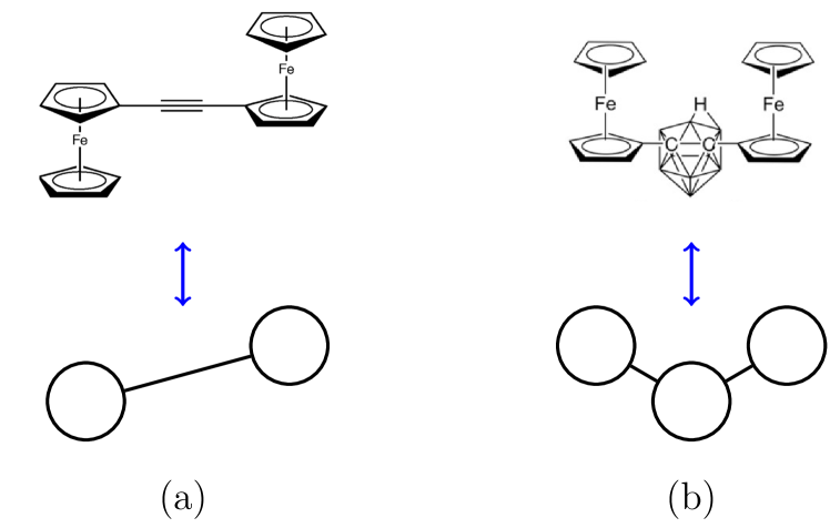
This paper focuses on molecular QCA [3, 22]. Here, an individual mixed-valence molecule functions as a cell, with redox centers on the molecule providing dots. One example of a QCA molecule is the diferrocenyl acetylene (DFA) [23, 5], as shown in Figure 2(a). Figure 2(b) shows a zwitterionic nido-carborane molecule [24], which provides a three-dot QCA cell. Like the atomic-scale dots [14], molecular QCA are helpful implementations because they allow bit energies that are robust at room temperature, eliminating the need for cryogenic cooling.
An important development in QCA is clocking, which enables the latching of bits onto cells [25], synchronous calculations, adiabatic circuit operation [16, 26, 27], and provides power gain for the restoration of weakened signals [28]. This may be achieved by adding a third pair of dots, as in Figure 3. The new dots provide a “Null” state with no information content. A potential may be applied to the central dots to clock the six-dot cell to the “Null” state; or, the polarity of that potential may be reversed to repel the mobile charge from the central null dots, clocking the six-dot cell to an active state, “0” or “1.” To switch a six-dot cell between active states requires an intermediate transition to the “Null” state. Thus, clocking a six-dot cell to an active state suppresses tunneling between active states and latches the bit on that six-dot cell. Logic may be formed from clocked six-dot cells as previously discussed.

In molecular QCA, a pair of three-dot molecules like the one shown in Figure 2(b) could be juxtaposed to function as a molecular clocked six-dot cell, as in Figure 3. The component of an applied electric field perpendicular to the device plane () may be used to clock the molecular devices and circuits [29, 30, 31].
In the remainder of this paper, we focus on three-dot molecules only. Three-dot molecules are useful because they can be arranged in circuits which interact with electric field like dipoles, providing a circuit with high sensitivity to the applied ; or they may be arranged to interact only weakly with the applied as quadrupoles. Additionally, we use the terms “cell” and “molecule” interchangeably.
III Model
The objective here is to explore the design and function of clocked QCA input circuits in the presence of unwanted electric fields. To do this, we develop a model for a circuit of clocked, three-dot molecular QCA immersed in an external electric field, . The time-independent Schrödinger equation is solved for the ground state of the circuit. The circuit will have succeeded when its ground state encodes the intended calculational result, and it will have failed when the ground state diverges from the correct output. First, the Hamiltonian, , of a single cell is introduced and validated in subsection III-A. Then, in subsection III-B, the non-interacting Hamiltonian, , for an -cell circuit is formed by summing all single-cell Hamiltonian operators . The circuit Hamiltonian, is completed by adding to an interaction term, . is calculated directly from electrostatics. The clocked input circuit is then introduced in subsection III-C. We limit the circuit size to , since larger circuits become intractable due to the exponential growth of the dimension of the circuit Hilbert space with : . Given the relatively small size of the molecular circuits treated here, we assume that the clocking electric field is uniform over the entire circuit.
III-A Molecular Device Description
Figure 4 provides a schematic depiction of a three-dot cell. The three molecular dots (black circles) are labeled 0, 1, and . The state is the localized state of one mobile electron (red disc) on dot . These are assigned device values “0,” “1,” and “Null,” respectively. States “0” and “1” represent a bit and are designated as “active states” of the molecular cell. Not depicted here is a fixed neutralizing charge, assumed to be located at the null dot. The neutralizing charge gives the molecule net charge neutrality, modeling a zwitterionic QCA molecule. For simplicity, the cell is treated as a system of two point charges: the mobile charge, , and the fixed charge, , where is the elementary charge. Black lines connecting dots represent tunneling paths for the mobile charge. As discussed above, direct tunneling between active states is suppressed, enabling the latching of a bit onto a cell. The active dots are separated by distance . Here, we will consider molecules adsorbed onto a surface (the plane) so that dot is on the surface and active dots are elevated to the plane .

Consider an isolated cell at position immersed in an electrostatic field , which is approximately constant over the volume of the cell. The Hamiltonian of the cell may be written as
| (1) |
where is a transition operator from to , and is a projection operator onto . The operator is analogous to the Pauli operator and employs the same sign convention for as in Ref. [32]. The first term in Equation (1) describes electronic tunneling between the active states and the “Null” state, and is characterized by , the hopping energy between either of the active states and the “Null” state. It is assumed that the molecule is symmetric so that describes both the transition and the transition. The second term in Equation (1) is characterized by , the detuning between states “0” and “1”:
| (2) |
The detuning may be separated into two components:
| (3) |
where is the bias due to the charge distribution of neighboring QCA cells, and is a bias driven by the applied field, . The field-driven bias is given by
| (4) |
where is the vector of length pointing from dot 1 to dot 0 (see Figure 4). The third term of Equation (1) is proportional to and describes the occupation energy of the “Null” state relative to the unperturbed active states. Here, the clock biases the “Null” state relative to the active states by the potential energy
and the energy describes the affinity the mobile charge has for the fixed neutralizing charge on dot . An biases the system toward the “Null” state. is a property of a particular QCA molecule, which may be estimated using quantum chemistry techniques or measured experimentally.
A cell’s charge state may be characterized by two real numbers: its polarization, , and its activation, :
| (5) | ||||
| (6) |
The sign of encodes a classical bit, and may be understood as the probability that the molecule will be measured in an active state.
We introduce the kink energy, , which is interpreted as the cost of a bit flip or the strength of a bit [33]. Consider a driver cell of characteristic length prepared in state . The kink energy for a target cell a distance away from the driver cell is the difference in energy between the target cell’s frustrated state and its relaxed state. Figure 5(a) shows the relaxed state, which is anti-aligned with the driver. In its frustrated state, the target cell aligns with the driver cell, as in Figure 5(b). The kink energy may be calculated directly using electrostatics:
| (7) |
where denotes the permittivity of free space.

In this paper, all calculations assume parameters , , , and . These parameters are chosen to represent a molecule like that of Figure 2(b). It is also assumed that the mobile charge is one electron, and that the fixed neutralizing charge is positive. For , .
The isolated cell’s ground state response to various applied fields is shown in Figure 6. In this plot, both the clocking component () and the biasing (input) component () of are scaled to , the field strength required to produce a kink in two cells, as in Figure 5(b):
| (8) |
In the absence of a clock (), or under weak clocking (), the cell remains in the null state (green region of the plot) because of the positive electron-hole affinity, . Therefore, some is required to clock the cell to an active state. If is large enough, even a weak input field () is adequate to select a bit on the cell (yellow and blue regions of the plot).

A QCA cell also may be driven by a neighboring molecule, as in Figure 7. Here, the response is calculated for a target cell in the presence of a fully-activated driver cell (). The target molecule’s response, , is plotted as a function of the driver polarization, , and the clocking electric field, . The -component of the field is zero here, since no external input field is applied. The repulsion by the driver cell’s mobile charge and the attraction to the driver cell’s neutralizing charge further bias the target cell toward the null state so that a stronger clock than before is required to activate the target cell. This effect has been termed “population congestion,” and has been studied in detail [34].

III-B Molecular Circuit Model
A convenient basis, , for an -cell circuit may be formed by taking the direct products of localized single-cell states:
| (9) |
Here, represents the -trit state , and labels a state of the -th cell.
The circuit Hamiltonian may be written as
| (10) |
where is the free Hamiltonian of the -th cell, and describes the interactions between neighboring cells. Here, is not included in , but rather is accounted for in . In the basis , the interaction is diagonal and may be written as:
| (11) |
Here, is the electrostatic energy of interaction between all cells given circuit state :
| (12) |
Integers and label a cell in the circuit, and they are chosen to avoid double-counting pairwise intercellular interactions or including unphysical, infinite self-interaction energies. The -th cell is treated as a system of point charges , with charges at positions . In the case of the mobile charges, depends on the state of cell . Positive integers and index the point charges consituting cells and , repsectively.
III-C Clocked Input Circuits

A clocked molecular QCA input circuit is shown in Figure 8(a). The molecular circuit consists of an input segment (cells 1-3) and a binary wire (cells 4,5,…).
The input segment also is referred to as a longitudinal array, since the cells are aligned along their longitudinal axes, the axis which points from one active dot to another. The minimal field-sensitive segment is two cells long. A longitudinal section of two or more cells has high sensitivity to the field component along its longitudinal axis, since each member cell interacts with the field as a dipole, aligning with both the field and one another. The input segment could be longer than three cells, but we limit its length to three cells in order to limit the dimension of the circuit Hamiltonian, as well as to provide a circuit with symmetry about the axis. This keeps the calculation manageable, and it allows the circuit to respond in a symmetric way to the input field, .
The binary wire is used to shift the bit selected on the input segment downstream to QCA logic for processing. The binary wire exhibits some insensitivity to the -component of the field, since adjacent cells tend to antialign, and pairs of cells interact with the field more weakly as quadrupoles. We refer to the binary wire as a shift register henceforth, because its constituent cells are able to latch bits under the clock.
There is no theoretical limit to the length of the shift register. An unclocked binary wire, on the other hand, is limited in length, since the entropy of a bit error (a kinked state) increases with the length of the wire, lowering the free energy of such errors [33]. For an adequately long wire, the free energy of a kink will fall below that of an error-free wire, giving rise to an error despite bit energies towering high above the thermal noise floor. A shift register, however, is actively driven by the clock: it is not in thermal equilibrium, and the clock provides power gain to restore weakened signals. Thus, a shift register can be longer than an unclocked wire [35].
The clocked input circuit is a synchronous version of the ballistic input circuit developed previously [8]. To select the input bit, the input circuit is immersed in an applied electric field parallel with the input section. The field may be established using input electrodes. This circuit is similar to an input from a proposals in which electrodes establish an electric field to write a bit onto a single molecule [7], but is designed to support input electrodes lacking single-molecule specificity. Previously, the clocked circuit of Figure 8(a) was studied [9] using an intercellular Hartree approximation (ICHA) [36], which discards intercellular correlations. This model includes all intercellular correlations and treats the circuit exactly in the limit of three-state quantum devices.
In this paper, two limiting cases of the field are studied. First is an idealized limit, which we call the nano-electrode limit. Here, the input field may be constrained to only the input segment, as illustrated Figure 8(b). We also consider the large-electrode limit, in which the entire circuit is immersed in the input field, as in Figure 8(c). This represents the worst case, in which the -component of the unwanted fringing is as strong as the input intentionally applied to the input portion of the circuit. A more realistic situation is intermediate to these two limits: input electrodes establish an input across the input segment, and field fringing applies some to the downstream QCA circuitry. If the circuits function properly in the large-electrode limit, then it is reasonable to expect that the circuits will function properly in the more realistic, intermediate regime.
In this paper, circuits are limited to cells, since presently, calculations are unwieldy for . Given the small size of these circuits, we apply in all calculations a uniform clock to all cells, which approximates a clock having a negligible gradient over the circuit modeled.
IV Results
IV-A Clocked Input Circuit Response
The ground state response of a clocked input circuit is shown in Figure 9, and both the idealized and worst-case of fringing fields are considered. In the ideal case, the sign of the field selects the output bit of the circuit, which is taken here to be encoded on cell 6. The same holds true in the large-electrode limit; here, however, fringing fields disrupt circuit operation for . In this case, it is possible to apply an input field of strength , which is adequate to select a bit on the input+shift-register circuit, but too weak to drive a wrong state on the shift register. When , the field is strong enough to induce a kink between cells 2 and 4, so that the wrong bit propagates down the shift register (see insets in the lower left and uppper right of Figure 9). This result is consistent with the result previously published for a an unclocked input QCA circuit [8]. All calculations use a strong clocking field (), since a clock of this magnitude results in a strong output bit ().

An even stronger fringing input field (), can simply inject multiple kinks into the shift register, causing all cells to align with . We do not study the circuit up to this point, since it is only necessary to find where the first failure occurs in order to determine the limits of operation for this circuit.
IV-B Clocked Input Circuits - A More Robust Design
The vulnerability of the binary wire cells to the component of fringing input fields suggests a simple modification for more robustness: the binary wire cells may be rotated by , as shown in Figure 10. For the rotated cells (4, 5, 6, etc.), leads to so that the -component of the fringing input field cannot affect the detuning between their active states. Thus, the rotated cells provide a binary wire immune to the -component of the field, but the non-rotated cells (1-3) retain their sensitivity to .
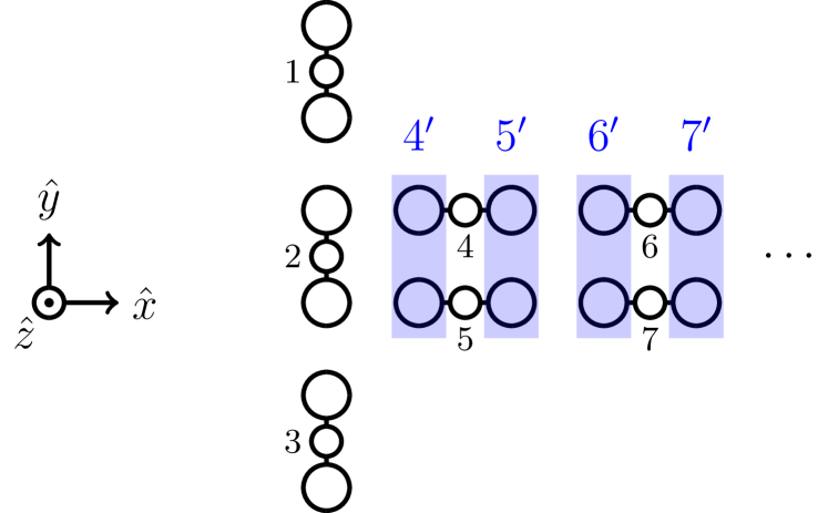
Results from the circuit of Figure 10 are shown in Figure 11. To obtain a result from this circuit directly comparable to the results of Figure 9, we group the active dots from the rotated molecular cells into functional cells, labeled etc. (see Figure 10). In particular, , the polarization of cell is plotted, where
| (13) |
Notably, the large-electrode response under unwanted fringing fields in the direction is identical to the nano-electrode response (ideal case), even under . The functional cell polarization remains unaffected by a strong fringing field with a -component, and the circuit will not fail, even under arbitrarily large values. As before, the clocking field was set to for all calculations.

In addition to immunity to fringing fields in the -direction, the input circuit and shift register of Figure 10 demonstrates robustness against fringing fields in the -direction. This is shown in Figure 12, where is plotted as a function of for various values of . Here, all calculations are in the large-electrode limit so that is applied to the entire circuit. The input field selects the input, and encodes the correct–albeit weakened–bit until . Circuit failure requires alignment between physical cells 6 and 7. Here, physical cells 6 and 7 align with the field and with one another (i.e., ) so that functional cell fails to an undesirable state: . Note that a bit weakened by an unwanted non-zero may be strengthened by increasing the strength of the clocking field, ; however, it is simplest and most illustrative to perform all calculations at a single clocking field strength, chosen here to be . We use a weaker clock than before, as it provides a more gradual onset of failure with increasing than in the case of the stronger .

A broader exploration of the effects of the component of the field on the circuit of Figure 10 is shown in Figure 13. Here, the blue and yellow regions are where the shift register functions properly: is strong and non-zero, despite some unwanted . The green region is where functional cells of the shift register fail to as the physical cells simply align with . In the absence of cells 6 and 7, the shift register (comprised only of cells 4 and 5) would fail when : here, the field has to do the work of injecting a kink between cells 4 and 5 (this is consistent with the result of Figure 8 of Ref. [8]). However, with the addition of cells 6 and 7, as in Figure 10, the attraction between neutralizing (mobile) charges in cells 4 and 5 and oppositely-charged mobile (neutralizing) charges of cells 6 and 7 lowers the energy of the configuration in which all shift register cells align with the field component . Thus, the shift register fails for . Similarly, in the absence of cells 6 and 7, a shift register comprised only of cells 4 and 5 would be resistant even to some fields , since the field must not only inject a kink, but also overcome the Coulomb repulsion between the mobile charge of cells 1-3 and the mobile charge of cells 4 and 5. Interactions between the (4,5) cell pair and the (6,7) cell pair lowers the field strength to for the onset of shift register failure. Nonetheless, the circuit tolerates significant non-zero, unwanted before the shift register fails: . Here, all calculations were performed using a clock of strength , although a stronger clock may compensate for the effects of to some extent.

It is reasonable to design the circuit for immunity to the component of fringing input electrode fields, but only tolerance to an unwanted non-zero component. The -component of fringing fields will be the dominant component applied over the innterconnecting shift register or even the down-stream logic, since the applied will be designed to be dominant in its component.
V Discussion
While this paper focuses on clocked molecular QCA inputs, it is worthwhile to contextualize it in the broader QCA paradigm and to briefly discuss open questions and challenges, especially those questions which pertain to this paper. We briefly mention the role QCA could play in general-purpose computing, and then discuss the open challenges of molecular design, synthesis, testing, circuit layout, and bit read-out.
If realized, molecular QCA could provide a room-temperature alternative to CMOS for both logic and memory. Device densities for cells with a footprint could approach , surpassing present-day CMOS densities by 3-4 orders of magnitude. Bits at this scale are very robust: bit energies of tower high above the thermal noise floor at room temperature, , eliminating the need for cryogenic temperatures. Molecular QCA operating speeds could approach the THz regime [5]. Clocked QCA support adiabatic operation for low power dissipation [16, 26, 37], and this will be important at the aforementioned device densities. Modeling and quantifying power dissipation in molecular QCA candidates is an area of development by other groups [27] as well as our own.
As a general-purpose computing paradigm, molecular QCA could deliver high performance at a low power demand in computing devices from wearables to supercomputers. Molecular QCA circuits could replace CMOS fully, or perhaps provide molecular processors that work along with CMOS, with the advent of suitable write-in and readout techniques for molecular circuits. In QCA, logic and memory may be intermingled, and non-von-Neumann architectures are possible [38, 39, 31].
Molecular design, synthesis, and testing are a crucial open questions in molecular QCA. Two-dot, three-dot, and four-dot molecules have been synthesized and probed using scanning-tunneling microscopy (STM), and charge-localized device states have been observed [23, 40, 41], along with field-driven switching [42]. Recently, control was demonstrated over the position of a mobile hole on a double-quantum-dot, bis-ferrocene cation using an atomic force microscopy (AFM) system [43]. This molecule is similar to the DFA molecule from Figure 2(a). Additionally, Henderson, et. al. [24], synthesized a new molecule in an important class of QCA candidates: zwitterionic, charge neutral, mxed-valence species [44, 45]. This type of molecule is self-doping so that its synthesis avoids the production of counter-ions. This is helpful because counter-ions will localize randomly near the ionic QCA cells, and such stray charge could disrupt circuit operation [46]. Progress in molecular QCA would be advanced if stable device charge states and switching/clocking were experimentally demonstrated in a neutral, mixed-valence QCA candidate. The design of neutral, mixed-valence species is an active research area for our research team.
To form circuits, non-homogenous patterns of molecules must be arranged on a surface. Promising techniques for molecular QCA circuit layout rely on self-assembly. Some works have explored the concept of bonding molecules to a gold substrate [47, 48]. Other proposals may combine top-down and bottom-up approaches, such as lithography and self-assembly. DNA rafts could be programmed with specific attachment sites for appropriately-functionalized QCA molecules, allowing for the self-assembled formation of molecular circuits on DNA circuit boards. This could allow suitable control over both the position and orientation of molecules. Top-down techniques such as electron-beam lithography (EBL) can define arrangements for the DNA circuit boards, providing a means for organization at a larger scale [49, 50, 51]. Indeed, exquisite control over DNA nanostructures has been demonstrated, both in 2D and 3D [52, 53]. To avoid unwanted effects from stray charge presented by phosphate groups in DNA structures, it may be helpful to develop peptide nucleic acid (PNA) circuit boards [54]. Experimental demonstrations of circuit layout—including adequate control of both cell placement and rotation—will be an important step forward in realizing molecular QCA.
QCA circuits may in fact allow for some lack of precision in the positioning and rotation of cells. QCA circuits can tolerate defects (i.e., missing cells, rotated cells, and displaced cells). Circuit robustness can be improved through techniques such as redundancy and clocking [55, 35, 47]. The circuit model presented here could be used to explore defect tolerance in circuits of limited size, and some approximations could be introduced to explore defects in larger circuits.
Additionally, the read-out of molecular QCA bits is an important technical challenge in QCA. Recent proposals for bit read-out involve the use of single-electron transistors (SETs) or single-electron boxes (SEBs) [56, 57, 58, 59]. While exquisitely sensitive, such these devices require low temperatures. A room-temperature read-out technique could be preferable to cryogenic read-out solutions. Our own research group is investigating room-temperature solutions and may be able to present some novel ideas in the near future.
Not only does this paper anticipate solutions to open questions identified above, but it also is written to invite and encourage further research and development toward achieving those solutions. The design and synthesis of QCA candidates is of strategic importance, since it is prerequisite to experimental demonstrations of output and input techniques. Circuit layout techniques could be demonstrated with QCA candidates, or even dummy molecules that do not provide QCA device states. Adequate circuit layout techniques will enable straight-forward, robust techniques for bit write-in to molecular QCA circuits. This work also suggests means by which molecular QCA logic could be designed to tolerate strong, unwanted electric fields.
VI Conclusion
We have extended a model of unclocked input circuits using two-dot QCA cells to a model of electric-field-clocked, three-dot QCA molecules. The circuit was treated exactly as a system of three-state QCA molecules. The clocked version of the originally-proposed input circuit from Ref. [8] operates even in the presence of unwatned fringing fields in the -direction. Strong fringing from the input field, however, can disrupt operation of the shift register portion of the circuit. Immunity to an arbitrarily large field component may be engineered in the shift register by rotating its constituent cells by 90∘. The rotated cells are no longer sensitive to the -component of the field, which is likely the strongest component of the field after the clocking component, . Additionally, the rotated cells demonstrate significant resilience to the component of the field, which is expected to be the weakest component in the fringing .
This highlights that the use of two orientations for the QCA cells may be useful for making some parts of the QCA circuitry sensitive to an applied input field () and other parts insensitive to the dominant component of the applied input field (). Importantly, it may be possible to operate clocked molecular interconnects and QCA logic circuits in the presence of unwanted fringing fields from input electrodes.
Other techniques may help to further minimize the effects of fringing input fields on QCA logic. Circuits could be engineered to maximize the spatial separation between logic and input circuits. Also, logic calculations could occur out of phase with input operations so that the input field components are minimized during logical computations. Finally, since input arrays are sensitive to even weak input fields, input fields strengths may be limited so that they cannot disrupt the operation of interconnects and logic. The extent to which logic tolerates unwanted electric fields is an active area of research for our group.
The robust circuits presented here provide a helpful step forward in developing viable solutions for bit write-in on molecular QCA circuits. Techniques for bit write-in are necessary if high-speed, energy-efficient general-purpose computation is to be realized using molecular QCA.
Acknowledgment
The authors thank Craig Lent of the University of Notre Dame for discussion on this work.
References
- [1] C. Lent, P. Tougaw, W. Porod, and G. Bernstein, “Quantum cellular automata,” Nanotechnology, vol. 4, p. 49, 1993.
- [2] G. L. Snider, O. Orlov, I. Amlani, G. H. Bernstein, C. S. Lent, J. L. Merz, and W. Porod, “A functional cell for quantum-dot cellular automata,” Solid-state Electronics, vol. 42, no. 7-8, pp. 1355–1359, Jul. 1998.
- [3] C. S. Lent, “Molecular electronics - bypassing the transistor paradigm,” Science, vol. 288, pp. 1597–1599, Jun. 2000.
- [4] C. Lent, B. Isaksen, and M. Lieberman, “Molecular quantum-dot cellular automata,” J. Am. Chem. Soc., vol. 125, pp. 1056–1063, Jan. 2003.
- [5] E. Blair, S. Corcelli, and C. Lent, “Electric-field-driven electron-transfer in mixed-valence molecules,” J Chem Phys, vol. 145, p. 014307, June 2016.
- [6] K. Walus, F. Karim, and A. Ivanov, “Architecture for an external input into a molecular qca circuit,” Journal of Computational Electronics, vol. 8, no. 1, pp. 35–42, March 2009.
- [7] A. Pulimeno, M. Graziano, D. Demarchi, and G. Piccinini, “Towards a molecular qca wire: Simulation of write-in and read-out systems,” Solid State Electron., vol. 77, no. 101-107, 2012.
- [8] E. Blair, “Electric-field inputs for molecular quantum-dot cellular automata circuits,” IEEE T. Nanotechnol., vol. 18, pp. 453–460, April 2019.
- [9] J. Henry, J. Previti, and E. Blair, “Electric-field bit write-in for clocked molecular quantum-dot cellular automata circuits,” in Proc. of the 2018 IEEE International Conf. on Rebooting Computing (ICRC 2018), 2018.
- [10] P. Tougaw and C. Lent, “Logical devices implemented using quantum cellular automata,” J. Appl. Phys., vol. 75, no. 3, pp. 1818–1825, Feb. 1994.
- [11] M. Niemier, M. Kontz, and P. Kogge, “A design of and design tools for a novel quantum dot based microprocessor,” in Proc. of the 37th Design Automation Conf., 2000, pp. 227–232.
- [12] C. Smith, S. Gardelis, A. Rushforth, R. Crook, J. Cooper, D. Ritchie, E. Linfield, Y. Jin, and M. Pepper, “Realization of quantum-dot cellular automata using semiconductor quantum dots,” SUPERLATTICES AND MICROSTRUCTURES, vol. 34, no. 3-6, pp. 195–203, SEP-DEC 2003, 6th International Conference on New Phenomena in Mesoscopic Structures/4th International Conference on Surfaces and Interfaces of Mesoscopic Devices, Maui, HI, DEC 01-05, 2003.
- [13] M. Macucci, M. Gattobigio, L. Bonci, G. Iannaccone, F. Prins, C. Single, G. Wetekam, and D. Kern, “A qca cell in silicon-on-insulator technology: theory and experiment,” Superlattice. Microst., vol. 34, pp. 205–211, 2003.
- [14] M. B. Haider, J. L. Pitters, G. A. DiLabio, L. Livadaru, J. Y. Mutus, and R. A. Wolkow, “Controlled coupling and occupation of silicon atomic quantum dots at room temperature,” Phys. Rev. Lett., vol. 102, p. 046805, 2009.
- [15] I. Amlani, A. Orlov, G. Snider, C. Lent, W. Porod, and G. Bernstein, “Experimental demonstration of electron switching in a quantum-dot cellular automata (qca) cell,” Superlattice. Microst., vol. 25, 1999.
- [16] G. Tóth, , and C. Lent, “Quasi-adiabatic switching for metal-island quantum-dot cellular automata,” J. Appl. Phys., vol. 85, pp. 2977–2984, 1999.
- [17] I. Amlani, A. Orlov, R. Kummamuru, G. Bernstein, C. Lent, and G. Snider, “Experimental demonstration of a leadless quantum-dot cellular automata cell,” Appl. Phys. Lett., vol. 77, pp. 295–297, 2000.
- [18] A. Orlov, R. Kummamuru, R. Ramasubramaniam, G. Toth, C. Lent, G. Bernstein, and G. Snider, “Experimental demonstration of a latch in clocked quantum-dot cellular automata,” Appl. Phys. Lett., vol. 78, pp. 1625–1627, 2001.
- [19] A. O. Orlov, I. Amlani, G. Toth, C. S. Lent, G. H. Bernstein, and G. L. Snider, “Experimental demonstration of a binary wire for quantum-dot cellular automata,” Applied Physics Letters, vol. 74, no. 19, pp. 2875–2877, May 1999.
- [20] I. Amlani, A. Orlov, G. Toth, G. Bernstein, C. Lent, and G. Snider, “Digital logic gate using quantum-dot cellular automata,” Science, vol. 284, pp. 289–291, 1999.
- [21] R. Kummamuru, A. Orlov, G. Toth, J. Timler, R. Rajagopal, C. Lent, G. Bernstein, and G. Snider, “Power gain in a quantum-dot cellular automata (qca) shift register,” 2001, pp. 431–436.
- [22] M. Lieberman, S. Chellamma, B. Varughese, Y. Wang, C. Lent, G. Bernstein, G. Snider, and F. Peiris, “Quantum-dot cellular automata at a molecular scale,” Ann. N.Y. Acad. Sci., vol. 960, pp. 225–239, 2002.
- [23] R. Quardokus, N. Wasio, R. Forrest, C. Lent, S. Corcelli, J. Christie, K. Henderson, and S. Kandel, “Adsorption of diferrocenylacetylene on au(111) studied by scanning tunneling microscopy,” Phys. Chem. Chem. Phys., vol. 18, pp. 6973–6981, 2013.
- [24] J. Christie, R. Forrest, S. Corcelli, N. Wasio, R. Quardokus, R. Brown, S. Kandel, Y. Lu, C. Lent, and K. Henderson, “Synthesis of a neutral mixed-valence diferrocenyl carborane for molecular quantum-dot cellular automata applications,” Angewandte Chemie, vol. 127, pp. 15 668–15 671, 2015.
- [25] A. Orlov, I. Amlani, R. Kummamuru, R. Rajagopal, G. Toth, J. Timler, , C. Lent, G. Bernstein, and G. Snider, “Power gain in a quantum-dot cellular automata latch,” Appl. Phys. Lett., vol. 81, pp. 1332–1334, 2002.
- [26] C. Lent, M. Liu, and Y. Lu, “Bennett clocking of quantum-dot cellular automata and the limits to binary logic scaling,” Nanotechnology, vol. 17, pp. 4240–4251, 2005.
- [27] S. Pidaparthi and C. Lent, “Exponentially adiabatic switching in quantum-dot cellular automata,” J. Low Power Electron., vol. 8, no. 30, 2018.
- [28] J. Timler and C. S. Lent, “Power gain and dissipation in quantum-dot cellular automata,” J. Appl. Phys., vol. 91, no. 2, pp. 823–831, Jan. 2002.
- [29] K. Hennessy and C. S. Lent, “Clocking of molecular quantum-dot cellular automata,” Journal of Vacuum Science & Technology B, vol. 19, no. 5, pp. 1752–1755, Sep. 2001.
- [30] E. Blair and C. Lent, “An architecture for molecular computing using quantum-dot cellular automata,” in IEEE C Nanotechnol., vol. 1. IEEE, 2003, pp. 402–405.
- [31] ——, “Clock topologies for molecular quantum-dot cellular automata,” J. Low Power Electron., vol. 8, no. 3, p. 31, September 2018.
- [32] G. Mahler and V. Weberruss, Quantum Networks: Dynamics of Open Nanostructures, second, revised and enlarged ed. Springer, 1998.
- [33] C. S. Lent, P. D. Tougaw, and W. Porod, “Quantum cellular automata: the physics of computing with arrays of quantum dot molecules,” in Workshop on Physics and Computation, PHYSCOMP’94 Proceedings, 1994, pp. 5–13.
- [34] J. Retallick and K. Walus, “Population congestion in 3-state quantum-dot cellular automata,” J. Appl. Phys., vol. 127, no. 24, p. 244301, 2020.
- [35] M. Liu and C. Lent, “Reliability and defect tolerance in metallic quantum-dot cellular automata,” J. Electron. Test., vol. 23, pp. 211–218, 2006.
- [36] P. Tougaw and C. Lent, “Dynamic behavior of quantum cellular automata,” J. Appl. Phys., vol. 80, no. 8, p. 4722, 1996.
- [37] E. P. Blair, M. Liu, and C. S. Lent, “Signal energy in quantum-dot cellular automata bit packets,” J. of Comp. and Theor. Nanoscience, vol. 8, pp. 972–982, 2011.
- [38] C. Lent and B. Isaksen, “Clocked molecular quantum-dot cellular automata,” IEEE T. Electron. Dev., vol. 50, no. 9, pp. 1890–1896, Sep. 2003.
- [39] C. Lent, K. Henderson, S. Kandel, S. Corcelli, G. Snider, A. Orlov, P. Kogge, M. Niemier, R. Brown, J. Christie, N. Wasio, R. Quardokus, R. Forrest, J. Peterson, A. Silski, D. Turner, E. Blair, and Y. Lu, “Molecular cellular networks: a non-von neumann architecture for molecular electronics,” in Proceedings of the IEEE International Conference on Rebooting Computing. IEEE, Dec. 2016.
- [40] Y. Lu, R. Quardokus, C. Lent, F. Justaud, C. Lapinte, and S. Kandel, “Charge localization in isolated mixed-valence complexes: An stm and theoretical study,” J. Am. Chem. Soc., vol. 132, pp. 13 519–13 524, 2010.
- [41] N. Wasio, R. Quardokus, R. Forrest, S. Corcelli, Y. Lu, C. Lent, F. Justaud, C. Lapinte, and S. Kandel, “Stm imaging of three-metal-center molecules: Comparison of experiment and theory for two mixed-valence oxidation states,” Phys. Chem. C, vol. 116, pp. 25 486–25 492, 2012.
- [42] H. Qi, S. Sharma, Z. Li, G. Snider, A. Orlov, C. Lent, and T. Fehlner, “Molecular quantum cellular automata cells. electric field driven switching of a silicon surface bound array of vertically oriented two-dot molecular quantum cellular automata,” J. Am. Chem. Soc., vol. 125, pp. 15 250–15 259, 2003.
- [43] J. Berger, M. Ondráček, O. Stetsovych, P. Malý, P. Holý, J. Rybáček, M. Švec, I. Stará, T. Mančal, I. Starý, and P. Jelínek, “Quantum dissipation driven by electron transfer within a single molecule investigated with atomic force microscopy,” Nat. Commun., vol. 11, p. 1337, March 2020.
- [44] Y. Lu and C. Lent, “Self-doping of molecular quantum-dot cellular automata: mixed valence zwitterions,” Phys. Chem. Chem. Phys., vol. 13, pp. 14 928–14 936, 2011.
- [45] ——, “Counterion-free molecular quantum-dot cellular automata using mixed valence zwitterions: A double-dot derivative of the [closo-1-cb9h10] cluster,” Chem. Phys. Lett., vol. 582, pp. 86–89, Jul. 2013.
- [46] M. LaRue, D. Tougaw, and J. Will, “Stray charge in quantum-dot cellular automata: A validation of the intercellular hartree approximation.” IEEE T. Nanotechnol., vol. 12, no. 2, pp. 225–233, 2013.
- [47] A. Pulimeno, M. Graziano, A. Sanginario, V. Cauda, D. Demarchi, and G. Piccinini, “Bis-ferrocene molecular qca wire: Ab initio simulations of fabrication driven fault tolerance,” IEEE T. Nanotechnol., vol. 12, no. 4, pp. 498–507, 2013.
- [48] M. Graziano, R. Wang, M. Roch, Y. Ardesi, F. Riente, and G. Piccini, “Characterisation of a bis-ferrocene molecular qca wire on a non-ideal gold surface,” Micro Nano Lett., vol. 14, no. 1, pp. 22–27, 2019.
- [49] K. Sarveswaran, P. Huber, M. Lieberman, C. Russo, and C. Lent, “Nanometer scale rafts built from dna tiles,” in Proc. of the Third IEEE Conference on Nanotechnology, 2003, pp. 417–420.
- [50] K. Sarveswaran, W. Hu, P. Huber, G. Bernstein, and M. Lieberman, “Deposition of dna rafts on cationic sams on silicon [100],” Langmuir, vol. 22, no. 26, pp. 11 279–11 283, Nov. 2006.
- [51] W. Hu, K. Sarveswaran, M. Lieberman, and G. Bernstein, “High-resolution electron beam lithography and dna nano-patterning for molecular qca,” IEEE T. Nanotechnol., vol. 4, no. 3, pp. 312–316, May 2005.
- [52] P. Rothemund, “Folding dna to create nanoscale shapes and patterns,” Nature, vol. 440, pp. 297–302, 2006.
- [53] B. Wei, M. Dai, and P. Yin, “Complex shapes self-assembled from single-stranded dna tiles,” Nature, vol. 485, pp. 623–626, 2012.
- [54] P. Wittung, P. Nielsen, O. Buchardt, M. Egholm, and B. Norde´n, “Dna-like double helix formed by peptide nucleic acid,” Nature, vol. 368, pp. 561–563, 1994.
- [55] T. Wei, K. Wu, R. Karri, and A. Orailoglu, “Fault tolerant quantum cellular array (qca) design using triple modular redundancy with shifted operands,” in Proceedings of the 2005 Asia and South Pacific Design Automation Conference. ACM, Jan. 2005.
- [56] P. Lafarge, H. Pothier, E. Williams, D. Esteve, C. Urbina, and M. Devoret, “Direct observation of macroscopic charge quantization,” Z. Physik B - Condensed Matter, vol. 85, pp. 327–332, Oct. 1991.
- [57] H. Brenning, S. Kafanov, T. Duty, S. Kubatkin, and P. Delsing, “An ultrasensitive radio-frequency single-electron transistor working up to 4.2k,” J. Appl. Phys., vol. 100, p. 114321, 2006.
- [58] R. Joyce, H. Qi, T. Fehlner, C. Lent, A. Orlov, and G. Snider, “A system to demonstrate the bistability in molecules for application in a molecular qca cell,” in IEEE Nanotechnology Materials and Devices Conference. IEEE, 2009.
- [59] Y. Lee, V. Joshi, A. Orlov, and G. Snider, “Si single electron transistor fabricated by chemical mechanical polishing,” J. Vac. Sci. Technol. B, vol. 28, no. C6L9, Nov. 2009.
![[Uncaptioned image]](https://cdn.awesomepapers.org/papers/ddc3bcdd-a6a1-4d04-a030-0c6a84971be4/Cong_portrait.jpeg) |
Peizhong Cong is Ph.D. candidate in the Department of Electrical and Computer Engineering at Baylor University. He received his B.S. (2013) from Tianjin University, M.S. (2016) from University of Rochester. He joined Dr. Enrique P. Blair’s research group in 2017. He focus his research on classical molecular computing using quantum-dot cellular automata (QCA); molecular QCA circuit design; and clocked molecular QCA. |
![[Uncaptioned image]](https://cdn.awesomepapers.org/papers/ddc3bcdd-a6a1-4d04-a030-0c6a84971be4/Blair_portrait.jpg) |
Enrique P. Blair (Senior Member, IEEE) is an associate professor in the Department of Electrical and Computer Engineering at Baylor University. He received his B.S. (2002), M.S. (2004), and Ph.D. (2015) in Electrical Engineering from the University of Notre Dame. His research interests include open quantum systems and classical molecular computing using quantum-dot cellular automata (QCA); quantum computing using molecular charge qubits; and ab initio semiconductor device modeling. He served in the U.S. Navy from 2004-2010 as a submarine officer and an instructor at the U.S. Naval Academy in the Department of Electrical and Computer Engineering. He has been on faculty at Baylor University since 2015. |