Realization of all logic gates and memory latch in the SC-CNN cell of the simple nonlinear MLC circuit
Abstract
We investigate the State-Controlled Cellular Neural Network (SC-CNN) framework of Murali-Lakshmanan-Chua (MLC) circuit system subjected to two logical signals. By exploiting the attractors generated by this circuit in different regions of phase-space, we show that the nonlinear circuit is capable of producing all the logic gates, namely OR, AND, NOR, NAND, Ex-OR and Ex-NOR gates available in digital systems. Further the circuit system emulates three-input gates and Set-Reset flip-flop logic as well. Moreover, all these logical elements and flip-flop are found to be tolerant to noise. These phenomena are also experimentally demonstrated. Thus our investigation to realize all logic gates and memory latch in a nonlinear circuit system paves the way to replace or complement the existing technology with a limited number of hardware.
Exploiting the hopping of trajectories in different wells of nonlinear systems, it is found that these systems possess the ability to produce all kinds of logic operations. Specifically in the present work, we show that if one uses two square waves in an aperiodic manner as input to the SC-CNN based simple nonlinear Murali-Lakshmanan-Chua(MLC) circuit, the response produces all the logic gates and RS flip-flop which are also experimentally demonstrated. Our investigation to realize all the logic gates and memory latch in a nonlinear circuit system paves the way to replace or complement the existing technology with a limited number of hardware components.
I Introduction
Logic gates are building blocks of any digital circuit and computer architecture. In general, following Boolean algebra, the logic operations are performed by converting given two inputs into a single logical output. For any logic operation, both the inputs and outputs have two states, namely ’ON’ or ’TRUE’ and ’OFF’ or ’FALSE’ states Mano (2003). The reliability of logic operations depends on the reliable operations of systems chosen. Since the current demand for miniaturization of logic devices, speed of computation and low-power consumption devices, it is inevitable to design an appropriate system which is able to produce noise-immune gates. As a result, for the past two decades or more, several schemes are being proposed such as DNA/RNA computing Adleman (1994); Collier et al. (1999), quantum computing Ladd et al. (2010); Nielsen and Chuang (2002), nano computing Bachtold et al. (2001) and nonlinear dynamics based computing in order to replace or complement the existing computer architecture based on silicon chipsHopfield (1982); Sinha and Ditto (1998, 1999); Prusha and Lindner (1999); Murali et al. (2009a, b); Sinha et al. (2009); Guerra et al. (2010); Worschech et al. (2010); Zamora Munt and Masoller (2010); Zhang, Song, and He (2010); Bulsara et al. (2010); Singh and Sinha (2011); Dari et al. (2011a, b); Storni et al. (2012); Roychowdhury (2015); Kohar et al. (2017); Venkatesh, Venkatesan, and Lakshmanan (2017a, b); Neves, Voit, and Timme (2017); Kia, Lindner, and Ditto (2017); Murali et al. (2018); Manaoj Aravind, Murali, and Sinha (2018); Sathish Aravindh, Venkatesan, and Lakshmanan (2018); Sathish Aravindh et al. (2020). Among these methods, nonlinear dynamics based computing can make reliable and re-configurable computer architecture because the underlying nonlinear systems posses a large number of basic functions.
Utilizing the flexibility of nonlinear dynamical systems for storing, communicating and processing of information in computer architecture has been an active area of research in nonlinear dynamics. In this connection, Hopfield had constructed a memory device using artificial neural network to store and retrieve information Hopfield (1982). Sinha and Ditto proposed a chaos-computing scheme to emulate different logic elementsSinha and Ditto (1998, 1999). In an optimal window of noise, it was observed the possibility of occurrence of logic behavior and this phenomenon is termed as logical stochastic resonance(LSR)Murali et al. (2009a, b); Sinha et al. (2009); Bulsara et al. (2010). The present authors employed strange nonchaotic attractors to build dynamical logic gates Sathish Aravindh, Venkatesan, and Lakshmanan (2018); Sathish Aravindh et al. (2020); Sathish Aravindh, Venkatesan, and Lakshmanan (2020). Besides, self-sustained oscillators can function as latches and registers if Boolean logic states are associated with the phases of the oscillator signalsRoychowdhury (2015). Heteroclinic computing is another nonlinear phenomenon based computation using a collective system of nonlinear oscillators Ashwin and Borresen (2004, 2005).
Not only nonlinear dynamics based computing complements existing silicon based technology, there also exist several efforts to extend computation techniques to other domains such as opticalSingh and Sinha (2011), chemicalSinha et al. (2009); de Lacy Costello et al. (2009); Stevens et al. (2012), physicalSathish Aravindh, Venkatesan, and Lakshmanan (2018), mechanicalMahboob et al. (2011), biologicalGerstung, Timmer, and Fleck (2009); Ando et al. (2011), molecularCollier et al. (1999); Kompa and Levine (2001) and other areas of scienceMotoike et al. (2001); Sinha, Munakata, and Ditto (2002); Norrell and Socolar (2009); Zhang, Song, and He (2010); Mozeika, Saad, and Raymond (2010); Zhang et al. (2012); Miyamoto et al. (2010). Instead of needing multiple hardware for different types of computations, nonlinear dynamical systems can act as processors of a flexibly configured and reconfigured device to produce different logic gates Worschech et al. (2010). In practice, the generation of nonidealitic and ambient noise restricts the ability to obtain different logic gates in these systems Murali et al. (2009b). Thus it is essential to choose appropriate nonlinear-dynamics based computing systems to overcome these odds.
Further, most of the previous studies have focused to produce OR(NOR) and AND(NAND) logic gates Sinha and Ditto (1998, 1999); Prusha and Lindner (1999); Murali et al. (2009a, b); Kohar and Sinha (2012); Kohar, Murali, and Sinha (2014); Kohar et al. (2017); Venkatesh, Venkatesan, and Lakshmanan (2017a, b); Sathish Aravindh, Venkatesan, and Lakshmanan (2018); Sathish Aravindh et al. (2020). Obtaining Ex-OR (simply XOR) and Ex-NOR (XNOR) in dynamical systems are equally important since these gates are the basis of ubiquitous bit-by-bit addition Storni et al. (2012). A half adder consists of an XOR gate and AND gate. Other uses of XOR gate include subtractor, comparator and controlled inverter. XOR and XNOR gates are usually obtained by the concatenation of NOR and NAND gates.
In the literature, it has been shown that in several nonlinear-dynamics based concepts like chaos computing Ditto, Murali, and Sinha (2008), heteroclinic network for computation Ashwin and Borresen (2004, 2005); Bick and Rabinovich (2009); Schittler Neves and Timme (2012); Neves, Voit, and Timme (2017), etc. the richness of nonlinear dynamics can be exploited to obtain flexible and reconfigurable logic gates including XOR gates. In this connection, Sinha et al. have demonstrated the flexible parallel implementation of logic gates using chaotic elements Sinha, Munakata, and Ditto (2002). Peng et al. have explored piecewise-linear systems to construct all dynamical logic gates Peng et al. (2008, 2010). Campos-Canton et al. have reported electronics experiments to obtain NOR, NAND and XOR gates in a piece-wise linear system Campos-Cantón et al. (2010). In ref.Cafagna and Grassi (2006); Campos-Cantón et al. (2012a) the equation of the plane in analytical geometry has been used to build a contribution of SR flip-flop and basic logic gates Cafagna and Grassi (2006); Campos-Cantón et al. (2012a). Storni et al. have investigated LSR by extending the analysis to a three well potential to realize XOR logic gates Storni et al. (2012). In ref.Canton, Martienz, and Duron (2017), the authors have proposed a method and circuit for integrating a programmable matrix in the field of reconfigurable logic gates employing a nonlinear system and an efficient programmable rewiring Canton, Martienz, and Duron (2017). Also Campos-Canton et al. have reported a parameterized method to design multivibrator circuit via Chua’s circuit system Campos-Cantón et al. (2012b).
Further, Murali et al. have shown that if one applies two low amplitude square waves as inputs to a two-state system, the response of the system produces a logical output (NOR/OR) with a probability controlled by the interplay between noise and bistable dynamics of the system. That is the interplay of nonlinearity and noise produces a flexible and realizable logic behavior. The authors have termed this phenomenon as Logical Stochastic Resonance (LSR) Bulsara et al. (2010). For the past few years LSR has been realized in many nonlinear systems such as a nanoscale device Guerra et al. (2010), resonant tunnel diodes Worschech et al. (2010), a vertical cavity surface emitting laser Zamora Munt and Masoller (2010); Zhang, Song, and He (2010), a polarization bistable laser Singh and Sinha (2011), a chemical system Bulsara et al. (2010), synthetic gene networks Dari et al. (2011a), and so on. Recently, two of the present authors along with Venkatesh employed coupled dynamical systems to build dynamical logic gates by altering the value of the logic inputs Venkatesh, Venkatesan, and Lakshmanan (2017b, a).
Also Gupta et al. have examined the possibility of noise free LSR by driving a two-stable system with periodic forcing instead of random noise Gupta et al. (2011). Kohar et al. have found that periodic forcing enhances the LSR in noisy bistable systems with periodic forcing instead of random noise Kohar, Murali, and Sinha (2014). By replacing noise with high-frequency harmonics, Venkatesh et al. realized logic operations AND, OR and RS flip-flop in the MLC circuit and they termed this phenomenon as Logical Vibrational Resonance (LVR). LVR has been realized in a two-potential system Venkatesh and Venkatesan (2016); Venkatesh, Venkatesan, and Lakshmanan (2017b, a). Besides logic gates, LSR and LVR can be used to realize SR flip-flops Gui et al. (2020a, b); Vincent et al. (2021); Murali et al. (2021). Then the question arises whether LSR and LVR can produce all the logic gates including XOR gate when one employs a bistable system. One finds that practically this is not possible. The reason for this shortcoming is the bistable nonlinearity of the system. For this case all the logic gates are obtained by assuming that for the input state , the response of the bistable system resides in the left well and for the input state it is in the right well and for the other input state it may be any one of the wells depending upon the logic operations chosen. With these assumptions, bistable nonlinear systems are well suited for producing OR/NOR and AND/NAND logic gates. However these assumptions are not sufficient enough to obtain the other logic gates, namely the XOR and XNOR gates. For example, an XOR gate admits a high logic output only if the inputs are at different logic levels [(0,1) or (1,0)] and low logic output only if the inputs are at the same logic level [(0,0) or (1,1)]. For this logic gate case, the assumption for obtaining logic gates in bistable nonlinear systems leads to a possible loss of information and further the bistable nonlinear systems are unable to hold the condition for XOR/XNOR logic gates. Thus, the bistable system is unable to produce XOR/XNOR gates. In this paper, we propose a solution by considering a three-well potential problem so as to implement all the logic elements including XOR gates.
It was also shown in several studies that the three well potential nonlinear systems which exhibit logical behaviors are better suited for computational purpose than the logical gates generated by the traditional bistable nonlinear systems when one considers aspects such as noise interference, waveform smoothness and bit error rate Lu et al. (2019); Liu and Liu (2014). Thus it is important to ask the question whether one can realize all the logic gates and memory latches in a single nonlinear circuit system. We address this issue in this paper.
We consider a State-Controlled Cellular Neural Network (SC-CNN) based Murali-Lakshmanan-Chua’s (MLC) circuit Günay (2010, 2010); Swathy and Thamilmaran (2014). This circuit is constructed by using two CNN cells and external forces including sinusoidal force, biasing and noise. The existing MLC consists of Chua’s diode and a linear resistor, a linear capacitor, and an inductor. The discrete inductor restricts the circuit for fabrications of ICs. Further, CNN is well suited when extending the analysis to the coupled system. Thus SC-CNN MLC is more advantageous than existing MLC in the aspects of hardware realization. We show that this nonautonomous oscillator when subjected to two aperiodic logical signals produces all the logic gates available in digital electronics. We also show that these logic gates are tolerant for an optimal range of noise intensity. Besides, it is reported that the fundamental logical behaviors such as OR/AND/XOR gates can be observed through one of the state variables of the circuit and for the realization of the complimentary logical operations NOR/NAND/XNOR gates the other state variable can be utilized. Further, we report the possibility of the occurrence of both high active SR flip-flop and low SR flip-flop as well because of the parallelism innate in this circuit. One can also further realize three-input gates in the circuit.
This paper is organized as follows. We discuss the dynamical mechanism for the implementation of logical gates in the three well potential system and present a basic study of the SC-CNN cell of the Murali-Lakshmanan-Chua’s (MLC) circuit in Sec.III and Sec.III, respectively. We present the experimental realization of CNN cell of the MLC circuit in Sec.IV. We also describe the experimental and numerical results for the realization of OR/NOR and AND/NAND gates, Exclusive-OR (XOR) and Exclusive-NOR (XNOR) logic gates, Set-Reset memory latch, effect of noise and three input gates in Sec.V. Finally, we conclude our analysis in Sec.VI.
II Dynamical mechanism for the implementation of logical gates in three well potential system
Consider a general nonlinear system
| (1a) | ||||
| Eq.(1a) can also be rewritten as | ||||
| (1b) | ||||

Here is a potential function of the nonlinear system. Assume that the potential is three well. It has three potential wells and two potential barriers as shown in Fig.1. Here , , and are the bias value, logical input value, Gaussian white noise with intensity ‘’, and the amplitude of external periodic forcing, respectively. The system (1) is driven by two square wave signals, namely and , which encode the logical inputs and the response of the system (1) is considered as the logical output. For example, the inputs and take the value for the binary logic number ‘1’ and for the binary logical value is ‘0’. Then, the four possible combinations viz. (0,0), (0,1)/(1,0) and (1,1) of the input streams are merged into three distinct values as . Thus, the resultant input signal is a three level aperiodic wave form. Depending on the logic input, the potential function of the system assumes three different forms. The output of logic gates is given by the well in which the state variable ‘x’ resides. More precisely, for OR gate if ‘x’ resides in the left well, we set the logic output as ‘0’, and ‘1’ if it resides in any of the center-well or right-well. In the XOR gate, the ON output is possible if one and only if one of the inputs to the gate is in the ON state. That is if both the inputs are ON states or both are OFF, an OFF output results. In this circumstance, a bistable system is not able to hold the three input states. Hence when we use a bistable nonlinear system for these kind of cases, it leads to an effective loss of information. To take care of this problem, we propose a solution by generalizing the chosen system from a bistable one to a three well potential system as described above. In particular we extend the scope of implementing the logic gates by increasing the numbers of potential wells in order to extend the possible input-output associations. For example, for the XOR gate we set the output to be logical ’1’ if the state value of the system lies between the two local maxima of the potential function, and it is assumed to be the logical value ’0’ otherwise. For the XNOR gate we set the output to be logical value ’0’ if the state of the system resides between the two local maxima of the potential function of the system and it is to be ’1’ if it resides anywhere in the other two potential wells. The truth table (see Table 1) for different input-output combinations is defined and summarized in Table.2.
| Logic Gates | (0,0) | (0,1)/(1,0) | (1,1) |
|---|---|---|---|
| AND | 0 | 0 | 1 |
| NAND | 1 | 1 | 0 |
| OR | 0 | 1 | 1 |
| NOR | 1 | 0 | 0 |
| XOR | 0 | 1 | 0 |
| XNOR | 1 | 0 | 1 |
| Logic Gates | Left well | Center well | Right well |
|---|---|---|---|
| AND | OFF | OFF | ON |
| NAND | ON | ON | OFF |
| OR | OFF | ON | ON |
| NOR | ON | OFF | OFF |
| XOR | OFF | ON | OFF |
| XNOR | ON | OFF | ON |
III SC-CNN cell of Murali-Lakshmanan-Chua’s (MLC) circuit
Cellular Neural Network (CNN), introduced by Chua and Yang in 1988 Chua and Yang (1988), is a n-dimensional array of circuit elements of analog components such as OP-amps, resistors, and capacitors . It is constructed by a large number of intercoupled identical dynamical systems called cells. These cells or nodes are essentially modeled by nonlinear ordinary differential equations. CNN is a relatively simple structure and is easy to be implemented by appropriate electronic circuit. Thus it is a powerful tool for the emulation and implementation of nonlinear dynamical systems having complex dynamics. A generalization of the CNN paradigm in which the CNN cells locally share their outputs as well as their state variables with each other was introduced by Arena Arena et al. (1995). This generalization exploits an analog architecture of CNN known as State Controlled-CNN (SC-CNN). Many studies have been reported on designing and implementation of chaotic circuits in terms of SC-CNNs Günay (2010); Swathy and Thamilmaran (2014); Luo and Wang (2016). The advantages of a SC-CNN are that they are inductorless and are RC based circuitry only, thereby leading to the realization of hardware and VLSI implementations Manganaro, Arena, and Fortuna (2012). The other significant applications of these kind of CNNs are parallel computing and low-power consumption. With these motivating facts, in this paper we consider an SC-CNN frame work of the well known MLC circuit. This circuit is essentially perturbed by two aperiodic square waves and as a consequence we show that the resultant output exhibits parallel logic elements and memory latch. In order to discuss this framework further, we first consider the MLC circuit as shown in Fig.2.


It is an established fact in Murali, Lakshmanan, and Chua (1994); Lakshmanan and Rajasekar (2003) that the normalized form of the well known MLC circuit equation can be written as
| (2a) | ||||
| or equivalently as | ||||
| (2b) | ||||
Here the overdot indicates time differentiation.
where
| (3) |
The relationships between the various circuit variables and circuit parameters and the above dynamical variables and parameters can be obtained from Ref.Murali, Lakshmanan, and Chua (1994); Lakshmanan and Murali (1996); Lakshmanan and Rajasekar (2003). Earlier studies on the dimensionless version of the circuit when the parameters were fixed at and were made. The quantity was varied in these studies Murali, Lakshmanan, and Chua (1994); Lakshmanan and Rajasekar (2003). The circuit exhibits various underlying dynamical features including period-doubling route to chaos, intermittent route, strange non-chaotic attractors (SNA), etc Lakshmanan and Murali (1996); Lakshmanan and Rajasekar (2003). Three of the present authors have also shown that when the quasiperiodically driven MLC circuit is subjected to two aperiodic and logical square waves, it reproduces logical response in both the SNAs and chaotic regimes of the circuit. The authors have shown that how these attractors are tolerant to noise, so that even one can emulate different logic functions Sathish Aravindh et al. (2020).
Following the work of Arena Arena et al. (1995), the SC-CNN associated with the MLC circuit can be generalized by the following dimensionless nonlinear state equations,
| (4) |
In Eq.(4), j is the cell index, and are the state variables and the cell outputs, respectively. Each represents a constant parameter and is the threshold value. Also in Eq.(4) and are linear combinations of the outputs and state variables, respectively, of the connected cells. A dynamic model of two generalized CNN cells corresponding to Eq.(4) can be defined as follows:
| (5) |
where and are state variables, and and are the corresponding outputs. The MLC circuit equation defined by Eq.(2) can be derived from Eq.(4), by assuming : , , , , , , , , and .
Consequently, from Eq.(4) the SC-CNN based MLC circuit model is organized as below :
| (6) |
Here and , corresponding to two logic inputs, is the bias and the remaining parameters are fixed at , , , and . The MLC circuit in the framework of SC-CNN has been studied numerically, experimentally and analytically in ref.Günay (2010). The standard MLC circuit (Fig.2) consists of a nonlinear resistor which has the three-segment piece-wise characteristics of Chua’s diode, a linear resistor, a linear inductor, and a linear capacitor with sinusoidal voltage source. On the other hand the SC-CNN model of MLC circuit (see Fig.3) mainly consists of a few OP-AMPs along with RC based circuits. Thus the SC-CNN model of the MLC circuit is an inductor-less purely RC based circuit, which leads to the realization of hardware easily. In the present paper, we consider this circuit and investigate the effect of two aperiodic and logical square wave signals on the SC-CNN of MLC circuit.
IV Experimental realization of CNN cell of MLC
Fig.3 represents the complete experimental setup for two SC-CNN cells which generate the dynamics of the SC-CNN based MLC circuit. It is clearly obvious from Fig.3, that the circuit consists of a CNN with two cells, corresponding to the dynamical variables in Eq.(6). The two state variables and of Eq(6) are associated with the voltages across the two capacitors and , respectively. The nonlinearity is simply implemented by taking into account the saturation of op-amps.
The circuit realization of the SC-CNN based MLC circuit is achieved with the cell components: and active element type voltage op-amps with supply voltages. All the experimental results are obtained by using Agilent (33220A) function generators and Agilent digital oscilloscope (DSO 7014B). The amplitude of the forcing signal is used to study the dynamics of the CNN based model.
V Experimental and Numerical results
V.1 Three level logic input
Now, we analyze the response of the system (6) to deterministic logic input signal . Specifically, we drive the system (6) with a low/moderate amplitude signal with two square waves of strengths and encoding two logic inputs. The inputs can be either 0 or 1, giving rise to four distinct logic input sets and . For a logical ‘’, we set , whereas for a ‘’, we set , where represents a small/moderate intensity input signal. As , the input signal sets (0,1) and (1,0) provide the same input signal . As a consequence, the input signals take the values and corresponding to the input sets or and , respectively.


For example, if then both the inputs for logical input ‘’ and values when it is ‘’. Figs.4(a) & 4(b) correspond to input signals & I2, Fig.4(c) is a three-level square wave. Here, as , the amplitude value of the wave is for input sets , 0 for input sets or and for the input set . Then the output of the appropriate logic gate is determined by the well in which the dynamical variable or resides. More specifically, for the OR/NOR and AND/NAND logic operations, the state variables hop between the left and right/center wells depending on the input streams, whereas for the XOR/XNOR logic gates, the state variables leap among all the three wells equally.

V.2 Realization of OR/NOR and AND/NAND logic gates
Two typical logical operations in digital circuits are OR and AND or the complementary gates NOR and NAND. To realize these gates, at least two inputs need to be converted into a single output. For example, in the case of OR logic operation, at least one of the two inputs is an ’ON’ state, so as to get an ’ON’ output, while for AND logic operation, it is essential to be in the ’ON’ for both the inputs, so as to obtain an ’ON’ output(see Table.2). The logical response of a desired type can be extracted by finding the solution of state variables and from (6). One can define or extract an appropriate gate by considering the state variables and in the phase space. For example, in our system (6), the system oscillates in three regions: namely 1) region - the state variable resides in the region , 2) region - the state variable oscillates between and 3) region - the state variable exists for .


Next to obtain the OR logic operation, when the state variable is in the region of the system (6), the output state is assumed to be the logical output value ’0’ and when the state variable resides in any one of the regions and , the output is assumed to be the logical value ’1’. With this input-output association, we solve equation (6) numerically by fixing the parameters as , and the remaining parameter values are assigned the same values as given in section III.
Now, we analyze the attractors of the system (6). In Fig.5, it is obvious that for input signal which corresponds to either (1,1) or (0,1)/(1,0) states, the response of the system ‘’ hops either in the region or in the positive side of region of the phase space and when the input signal is in the (0,0) state, the value of the state variable ‘’, is in other segment, namely the region. The logical output is ‘’ when and it is ‘0’ for . As a consequence, for the two sets of input streams (1,1) and (0,1)/(1,0), the attractor of the system is bounded in region and its is region for the (0,0) state. This confirms the fact that the dynamical attractor is although chaotic, it behaves as the logical OR operation. It is also interesting to note in Fig.5 that when , the variable of the attractor is bounded in the region . That is the response of the variable turns out to be the inverted output of the variable. As a result, these two variables and produce logic gates OR and NOR in parallel in this circuit.
These results are clearly illustrated in the time trajectory plot as shown in Figs.6. In Fig.6(a) the three level diagram for the logic input is shown and as the bias value ‘’ is changed from to (see Fig.6(b)) the response of the system morphs from OR gate to the other logical AND gate in the regime of Fig.6(c) and the corresponding logic output as shown in Fig.6(d). For this case, it is found that for the (1,1) state, the attractor is in the region of phase space while for (0,1) /(1,0) and (0,0) state it is either in the negative region or in the region. Hence, switching the bias value from +0.01 to -0.01 morphs logical OR gate to logical AND gate (see Figs.6(c) & 6(d)). In a similar fashion the other state variable mimics the inverted output signal of , thereby produces a clean logical NOR for bias value . It is further observed that the response of state variable of the system morphs from NOR logic to NAND logic (see Figs.6(e) & 6(f)) when the threshold switches from the value of 0.01 to -0.01. Thus the system (6) produces logic OR/AND through one of state variable while its complementary logic function NOR/NAND is realized via the other state variable .


Next we verify the numerical results discussed earlier in the electronic circuit analog of the nonlinear system described by Eq.(6) and ascertain its robustness in experiments. The complete circuit realization for the two SC-CNN cells generating the dynamics of SC-CNN MLC circuit is shown in Fig.3. As pointed out earlier, Fig.3 consists of two cells, each corresponding to one dynamical variable in Eqs.(6). The two state variables and of Eqs.(6) are associated with the voltages and across the two capacitors and , respectively. Now we fix , and corresponding to dimensionless units of the circuit parameter that we discussed earlier. The changes in the dynamics of the circuit under the effect of input streams are obtained by measuring the voltages and across the capacitors and , respectively. The logic input signals and are when the logic input is ‘1’ and for ‘0’ bias voltage . For this case, the response of the circuit exhibits OR gate when we measure the voltage across and NOR gate when we measure the voltage across (see Fig.7). In a similar way, for , the system gives the AND gate when the voltage is measured across and NAND gate when the voltage is measured across (see Fig.8). The logical output ‘’ in Figs.7(d)/7(h) & 8(d)/8(h) are obtained as by feeding the output response to an appropriate comparator circuit Campos-Cantón et al. (2010). Further, we can quantify the process of obtaining a given logic output by calculating as shown in Fig.9 in which it is observed that the fundamental logic operation OR is realized in an optimal width of forcing amplitude ‘’. It is interesting to note that the logic operation is realized for subthreshold input which results in an optimal window of forcing value where tends to .

V.3 Realization of XOR and XNOR logic gates
The logic gate XOR is quite different from the previously discussed gates AND, OR, NAND and NOR. XOR gates admit a logic output of ‘1’ or high logic level if the inputs are at different logic levels, that is either of 0 and 1 or 1 and 0. Conversely, the output will be a ‘0’ or a low logic if the inputs are at the same logic levels 0 and 0 or 1 and 1. The function of XOR gate is to start with a regular ‘OR’ gate. However, the output is inhibited from going to ‘1’ or high when both the inputs are high or ‘1’ and it takes logic low or ‘0’ even when both the inputs are high or ‘1’. For these conditions, a bistable nonlinear system fails to satisfy them. Since the system (6) has a three segment piece-wise continuous function, it results in the gradient of a triple well energy potential. As a result, the present system (6) has the ability to produce XOR and XNOR gates, apart from producing the fundamental logic gates OR,AND, NOR and NAND. To realize XOR, we set the output to be logical ‘1’ if the state variable lies in between and the output is assumed to be logic ‘0’ if the state variable resides anywhere else, that is, when the attractor of system (6) resides in the region, the response output is assumed to be high or ’1’ and ’0’ otherwise, when the attractor may be in the region or region (see Fig.10).


With this input-output correspondence, we solve the Eq.(6) numerically by fixing the system parameters as , and . It is clearly shown in the phase space diagram Fig.10 that for the (0,0) state the attractor of the system resides in the region of the phase space, for the input (0,1) or (1,0) states, it hops in between -1 to +1 in the region and for (1,1) state it is in the region. Thus for the state (0,1) or (1,0) the output response of the system is considered to be logical value ‘1’ since the state variable of the system hops in the region and for the other states (0,0) or (1,1) the response of the output is considered to be the logical value ‘0’ because the state variable oscillates either in the or in region depending on the input streams. Hence, the output response of the system admits a high logic output for inputs of different logic levels, either of 0 and 1 or 1 and 0, and it is a low logic output for the same logic levels, namely 0 and 0 or 1 and 1.
Thus for the above set of parameter values, the system (6) admits logic XOR gate. It is also clearly demonstrated in phase diagram (see Fig.10) that the response of the state variable turns out to be the inverted output of the other state variable . As a consequence, when the state variable produces the logical XOR gate, the other state variable produces the complementary gate, namely the logical XNOR gate. Thus the present system has the ability to produce XOR gate in one of the state variables and XNOR gate in other state variable parallely without altering any system parameter. These results are also illustrated in the time trajectory plots in Fig.11. In Figs.12(c), 12(d)& 12(g), 12(h), it is demonstrated how the response of the system variables and behave as logical XOR and XNOR operations, respectively, under different input streams as shown in Figs.12(a),12(b),12(e) and 12(f).
To substantiate our numerical simulations, we carried out the experimental realization of XOR and XNOR gates by using the analog circuit given in Fig.3. For this purpose, we fix the parameter values as , and corresponding to the dimensionless parameters. The logical XOR and XNOR responses are obtained by measuring the voltages and across the capacitors and , respectively. It is obvious from Fig.12 that the signals measured across and behave as logical XOR and logical XNOR operations under different three-level input streams. Thus our experimental study confirms the fact that the considered circuit system has the potential to produce not only the fundamental gates OR/NOR and AND/NAND, but it can also emulate the logical XOR and XNOR operations as well. The logical outputs ‘’ in Figs.12(d)/12(h) are obtained as by feeding the output response to an appropriate comparator circuit Campos-Cantón et al. (2010). Also, we can quantify the process of obtaining a given logic output by calculating as shown in Fig.13, where it is observed that the fundamental logic operation XOR is realized in an optimal width of forcing amplitude ‘’. It is interesting to note that the logic operations are realized for subthreshold input which results in an optimal window of forcing value where tends to .
V.4 Set-Reset Memory latch
| Set | Reset | Output | State |
| 0 | 0 | Q | Last state |
| 0 | 1 | 0 | Reset |
| 1 | 0 | 1 | Set |
| 1 | 1 | ? | Not allowed |


Apart from designing logic gates many efforts have been made to exploit nonlinear systems to construct memory devices. Chaos based SR flip-flop from two cross coupled Chua’s circuit, SR flip-flop using reconfigurable analog block, set-reset latch in noise assisted bistable system, R-S flip-flop from two-cross coupled quasiperiodically driven MLC circuit are few examples for constructing memory latch using nonlinear systemsCafagna and Grassi (2006); Campos-Cantón et al. (2012a); Venkatesh, Venkatesan, and Lakshmanan (2017b); Sathish Aravindh et al. (2020). In the present work, we demonstrate how the simple SC-CNN based periodically driven MLC circuit (6) can produce a consistent and complete RS flip-flop.
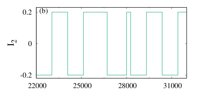
In this case, the input streams should be modified. It is quite obvious from the truth table of an SR flip-flop that (0,1) and (1,0) input sets are quite different, since these sets produce different output states (see Table.3). As a result we encode the inputs in a different way. Here the first input takes ‘1’ when the logic input is ‘+1’ while it is ‘0’ when the logic input is ‘0’. But the second input takes the value ‘1’ when the logic is ‘0’ while ‘0’ for logic ‘+1’. This could be achieved by applying the NOT operation to . For this case also the input streams and represent to values of and values. Here, set is a restricted one. For example, if , both the inputs -0.2 for logical input ‘’ and the values for logical input ‘’. The input signal is thus a three-level wave form : for (0,1), for (0,0)/(1,1) and for (1,0) inputs sets.
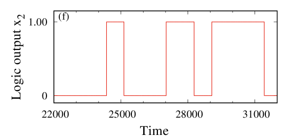
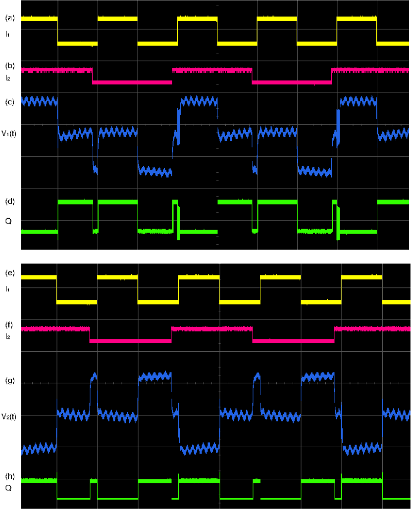
When we apply above mentioned input streams (Figs.15(a) and 15(b)) to the system (6), it is possible to realize the S-R flip-flop in the circuit. As usual, the logical output can be obtained by assuming that the output is to be the value ‘’ for and 0 if . S-R flip-flop operation is clearly shown in Figs.15(c) & 15(d) and 15(g) & 15(h). When and inputs are in the low states, it is found that the system response remains unchanged. When is in the low state and is in the high state, it is observed that the response of the system and hence it is assumed that the logical input is low. This makes the system as a latch with reset condition. When the input is in the high state while is low, it is realized that the output of the system is and thus it is assigned the logical value ‘’. In a similar way, the output of the dynamical variable (Fig.15(g)), provides the inverted output of Fig.15(c) and it behaves as an active high RS flip-flop. Usually in digital circuits, active low and active high RS flip flops are obtained by two cross coupled NAND and NOR gates. But in the present case, these two active high and low RS flip flops are obtained through two dynamical variables of the circuit. Hence the considered circuit is not only providing logical gates but also acts as a sequential circuit to provide RS flip flop operations of various categories such as active low and active high RS flip flops. To realize the Set-Rest latch experimentally, we design the system (6) with two inputs and . In the case of logic gates as discussed earlier, two inputs are added by an op-amp summing amplifier, whereas in the case of Set-Reset latch case, the two inputs are subtracted by an op-amp subtracting amplifier. In the circuit of Fig.14, the signal is generated by a set of op-amp summing amplifier by adding the resulting signal , external bias voltage, external noise signal and sinusoidal signal. Fig.16 verifies the Set-Reset latch behavior in our electronic circuit. The logical output ‘’ in Figs.16(d)/16(h) are obtained as by feeding the output response to an appropriate comparator circuit Campos-Cantón et al. (2010).
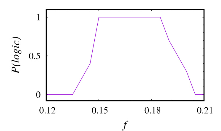
Further, we can quantify the process of obtaining a given logic output by calculating as shown in Fig.17 where it is observed the Set-Reset memory latch is realized in an optimal width of forcing amplitude ‘’. It is interesting to note that the logic operations which are realized for subthreshold input results in an optimal window of forcing value where tends to .


| Left well | Center well | Right well | |
|---|---|---|---|
| 0 0 0 | ON | OFF | OFF |
| 0 0 1 | OFF | ON | ON |
| 0 1 0 | OFF | ON | ON |
| 0 1 1 | OFF | ON | ON |
| 1 0 0 | OFF | ON | ON |
| 1 0 1 | OFF | ON | ON |
| 1 1 0 | OFF | ON | ON |
| 1 1 1 | OFF | ON | ON |
V.5 Logic responses even in three-input configuration
Next we consider the question whether we can extend the scope of this nonlinear circuit system to three inputs or higher inputs?. The answer is yes and we have found that without altering any of the parameters, the system (6) admits logic responses even when feeding three-inputs. In particular, the system produces logic behavior when we feed three inputs , and .
To be specific, for obtaining the OR gate, we fix the numerical parameters as , and (experimental parameters: , , , , and ). The first three panels of Figs.18 & 19 show the three different inputs while the fourth panel corresponds to logical OR dynamics. Hence for states (0,0,0) the output response of the system is assumed to be the logical ‘0’ since the state variable oscillates in the region and for other states the output response is to be logical ’1’ value because the state variable oscillates in the and regions [see Figs.18(d) & 19(d)] and also the corresponding logic output represent in Figs.18(h) & 19(e). The logical output ‘’ in Figs.19(d)/19(h) are obtained as by feeding the output response to an appropriate comparator circuit(see Table.4). Switching the bias voltage to , one can obtain three-input AND gate. However, three-input XOR and XNOR are not possible since the circuit is a three-segment piecewise linear system. To realize the three-input XOR and XNOR gates, one has to employ a minimum of four-well potential nonlinear system.

V.6 Effect of noise
Now, we investigate the effect of noise on the logic behavior of the circuit system (6). In particular, we ascertain the robustness of the logic response with respect to ambient noise. That is, we have to analyze whether the logic response persists even in the presence of noise or not. For this propose, we calculate the probability P(logic) of getting logic gates for different noise strength levels, with strength . Essentially P(logic) denotes the ratio of the total number of successful runs to the total number of runs. If the system exhibits the desired logic output in response to all the logic inputs, P(logic) is assigned a value ‘1’, otherwise it is treated as ‘0’. Our numerical simulation, P(logic) for the circuit (6), is obtained by sampling 1000 runs of the given input set and this process is repeated for 500 such sets. It is clearly indicated in Fig.20, that for noise strength , the system exhibits logic behavior. Beyond , the system loses its logic behavior. Thus, it is clearly demonstrated that the robustness of logical response of the system continues even in the presence of noise originating due to electronic components or any other external factors.
VI Conclusion
We have investigated the effect of logic square wave signals on the SC-CNN of MLC circuit system. Exploiting the hopping of attractors generated by this circuit, we have found that the circuit can emulate all basic logic operations corresponding to the logic gates OR, AND, NOR, NAND, XOR and XNOR and memory latch element RS flip-flop. It is also shown that all these logic behaviors are tolerant to noise. We have extended the scope of obtaining the logic gates by even feeding higher order inputs, specifically three-inputs. Results obtained by numerical simulations are in good agreement with experimental demonstration. Our study throws some useful light in replacing the existing computer technology with a minimal hardware.
It is clearly evident from our studies that the SC-CNN model of the MLC circuit can function as logic gates as well as memory latch even for small-amplitudes of the input signal. As a result, it consumes only a small power. Further, the same circuit can be used to produce a logic output corresponding to three-input logic. Thus this circuit may be used as two-input and three-input logic gates as well. The low active RS flip-flop and the high active RS flip-flop are constructed by cross-coupling of two NAND gates and cross-coupling of two NOR gates. Hence, the same MLC circuit can produce low active RS flip-flop through one state variable and high active RS flip-flop through another state variable. Further, the circuit can potentially operate in noisy environments.
Thus, the circuit can function not only in a noisy atmosphere but can also be capable of utilizing its resources by configuring the circuit into two-input, as well as three input gates and also as a memory device depending on the requirement. For instance, if we need to run a program, the circuit will mimic as logic gates of two inputs or three inputs, and on the other hand, for processing of data, the circuit will mimic as memory device which enables one to utilize it optimally. Apart from the computer architecture, the circuit morphs into a memory latch which may lead to acting as an electronic switching-de bouncer.
In this paper, we have proved that the underlying chaotic trajectories, which hop in different quadrants of the phase-space, induce parallel logic operations and memory latch in the SC-CNN of the MLC circuit and this feature may be considered for the replacement of currently existing processors and also as a remedy for Moore’s lawKia, Lindner, and Ditto (2017). Further one has to study the important features of this circuit such as access clock time, access energies and cell feature size and compare them with the existing technology, provide technically feasibility of the circuit for design and development of dynamic architecture. We hope to pursue these aspects in the near feature.
AUTHOR’S CONTRIBUTIONS
All authors contributed equally.
Acknowledgment
P.A. and A.V. acknowledge the DST-SERB for providing financial support for a research project under Grant No.EMR/2017/002813. M.S. sincerely thanks the Council of Scientific & Industrial Research, India for providing a fellowship under SRF Scheme No.08/711(0001)2K19-EMR-I. A.V. also acknowledges the DST-FIST for supporting experimental work under Grant No.SR/FST/College-2018-372(C). M.L. acknowledges the DST-SERB Distinguished Fellowship program under Grant No.SB/DF/04/2017 for financial support.
DATA AVAILABILITY
The data that support the findings of this study are available from the corresponding author upon reasonable request.
REFERENCES
References
- Mano (2003) M. M. Mano, Computer system architecture (Prentice-Hall of India, 2003).
- Adleman (1994) L. M. Adleman, “Molecular computation of solutions to combinatorial problems,” Science 266, 1021–1024 (1994).
- Collier et al. (1999) C. Collier, E. Wong, M. Belohradskỳ, F. Raymo, J. Stoddart, P. Kuekes, R. Williams, and J. Heath, “Electronically configurable molecular-based logic gates,” Science 285, 391–394 (1999).
- Ladd et al. (2010) T. D. Ladd, F. Jelezko, R. Laflamme, Y. Nakamura, C. Monroe, and J. L. O’Brien, “Quantum computers,” Nature 464, 45–53 (2010).
- Nielsen and Chuang (2002) M. A. Nielsen and I. Chuang, Quantum computation and quantum information (American Association of Physics Teachers, 2002).
- Bachtold et al. (2001) A. Bachtold, P. Hadley, T. Nakanishi, and C. Dekker, “Logic circuits with carbon nanotube transistors,” Science 294, 1317–1320 (2001).
- Hopfield (1982) J. J. Hopfield, “Neural networks and physical systems with emergent collective computational abilities,” Proc. Natl. Acad. Sci. 79, 2554–2558 (1982).
- Sinha and Ditto (1998) S. Sinha and W. L. Ditto, “Dynamics based computation,” Phys. Rev. Lett. 81, 2156 (1998).
- Sinha and Ditto (1999) S. Sinha and W. L. Ditto, “Computing with distributed chaos,” Phys. Rev. E 60, 363 (1999).
- Prusha and Lindner (1999) B. S. Prusha and J. F. Lindner, “Nonlinearity and computation: Implementing logic as a nonlinear dynamical system,” Phys. Lett. A 263, 105–111 (1999).
- Murali et al. (2009a) K. Murali, I. Rajamohamed, S. Sinha, W. L. Ditto, and A. R. Bulsara, “Realization of reliable and flexible logic gates using noisy nonlinear circuits,” Appl. Phys. Lett. 95, 194102 (2009a).
- Murali et al. (2009b) K. Murali, S. Sinha, W. L. Ditto, and A. R. Bulsara, “Reliable logic circuit elements that exploit nonlinearity in the presence of a noise floor,” Phys. Rev. Lett. 102, 104101 (2009b).
- Sinha et al. (2009) S. Sinha, J. Cruz, T. Buhse, and P. Parmananda, “Exploiting the effect of noise on a chemical system to obtain logic gates,” EPL (Europhysics Letters) 86, 60003 (2009).
- Guerra et al. (2010) D. N. Guerra, A. R. Bulsara, W. L. Ditto, S. Sinha, K. Murali, and P. Mohanty, “A noise-assisted reprogrammable nanomechanical logic gate,” Nano Lett. 10, 1168–1171 (2010).
- Worschech et al. (2010) L. Worschech, F. Hartmann, T. Kim, S. Höfling, M. Kamp, A. Forchel, J. Ahopelto, I. Neri, A. Dari, and L. Gammaitoni, “Universal and reconfigurable logic gates in a compact three-terminal resonant tunneling diode,” Appl. Phys. Lett. 96, 042112 (2010).
- Zamora Munt and Masoller (2010) J. Zamora Munt and C. Masoller, “Numerical implementation of a VCSEL-based stochastic logic gate via polarization bistability,” Opt. Express 18, 16418–16429 (2010).
- Zhang, Song, and He (2010) L. Zhang, A. Song, and J. He, “Effect of colored noise on logical stochastic resonance in bistable dynamics,” Phys. Rev. E 82, 051106 (2010).
- Bulsara et al. (2010) A. R. Bulsara, A. Dari, W. L. Ditto, K. Murali, and S. Sinha, “Logical stochastic resonance,” J. Chem. Phys 375, 424–434 (2010).
- Singh and Sinha (2011) K. P. Singh and S. Sinha, “Enhancement of “logical” responses by noise in a bistable optical system,” Phys. Rev. E 83, 046219 (2011).
- Dari et al. (2011a) A. Dari, B. Kia, A. R. Bulsara, and W. Ditto, “Creating morphable logic gates using logical stochastic resonance in an engineered gene network,” Europhys. Lett. 93, 18001 (2011a).
- Dari et al. (2011b) A. Dari, B. Kia, X. Wang, A. R. Bulsara, and W. Ditto, “Noise-aided computation within a synthetic gene network through morphable and robust logic gates,” Phys. Rev. E 83, 041909 (2011b).
- Storni et al. (2012) R. Storni, H. Ando, K. Aihara, K. Murali, and S. Sinha, “Manipulating potential wells in logical stochastic resonance to obtain XOR logic,” Phys. Lett. A 376, 930–937 (2012).
- Roychowdhury (2015) J. Roychowdhury, “Boolean computation using self-sustaining nonlinear oscillators,” Proceedings of the IEEE 103, 1958–1969 (2015).
- Kohar et al. (2017) V. Kohar, B. Kia, J. F. Lindner, and W. L. Ditto, “Implementing boolean functions in hybrid digital-analog systems,” Phys. Rev. Appl. 7, 044006 (2017).
- Venkatesh, Venkatesan, and Lakshmanan (2017a) P. R. Venkatesh, A. Venkatesan, and M. Lakshmanan, “Implementation of dynamic dual input multiple output logic gate via resonance in globally coupled Duffing oscillators,” Chaos 27, 083106 (2017a).
- Venkatesh, Venkatesan, and Lakshmanan (2017b) P. R. Venkatesh, A. Venkatesan, and M. Lakshmanan, “Design and implementation of dynamic logic gates and RS flip-flop using quasiperiodically driven Murali–Lakshmanan–Chua circuit,” Chaos 27, 033105 (2017b).
- Neves, Voit, and Timme (2017) F. S. Neves, M. Voit, and M. Timme, “Noise-constrained switching times for heteroclinic computing,” Chaos 27, 033107 (2017).
- Kia, Lindner, and Ditto (2017) B. Kia, J. F. Lindner, and W. L. Ditto, “Nonlinear dynamics as an engine of computation,” Phil. Trans. R. Soc. A 375, 20160222 (2017).
- Murali et al. (2018) K. Murali, S. Sinha, V. Kohar, B. Kia, and W. L. Ditto, “Chaotic attractor hopping yields logic operations,” PloS one 13, e0209037 (2018).
- Manaoj Aravind, Murali, and Sinha (2018) V. Manaoj Aravind, K. Murali, and S. Sinha, “Coupling induced logical stochastic resonance,” Phys. Lett. A 382, 1581–1585 (2018).
- Sathish Aravindh, Venkatesan, and Lakshmanan (2018) M. Sathish Aravindh, A. Venkatesan, and M. Lakshmanan, “Strange nonchaotic attractors for computation,” Phys. Rev. E 97, 052212 (2018).
- Sathish Aravindh et al. (2020) M. Sathish Aravindh, R. Gopal, A. Venkatesan, and M. Lakshmanan, “Realisation of parallel logic elements and memory latch in a quasiperiodically-driven simple nonlinear circuit.” Pramana 94 (2020), 10.1007/s12043-020-1939-4.
- Sathish Aravindh, Venkatesan, and Lakshmanan (2020) M. Sathish Aravindh, A. Venkatesan, and M. Lakshmanan, “Route to logical strange nonchaotic attractors with single periodic force and noise,” Chaos 30, 093137 (2020).
- Ashwin and Borresen (2004) P. Ashwin and J. Borresen, “Encoding via conjugate symmetries of slow oscillations for globally coupled oscillators,” Phys. Rev. E 70, 026203 (2004).
- Ashwin and Borresen (2005) P. Ashwin and J. Borresen, “Discrete computation using a perturbed heteroclinic network,” Phys. Lett. A 347, 208–214 (2005).
- de Lacy Costello et al. (2009) B. de Lacy Costello, R. Toth, C. Stone, A. Adamatzky, and L. Bull, “Implementation of glider guns in the light-sensitive belousov-zhabotinsky medium,” Phys. Rev. E 79, 026114 (2009).
- Stevens et al. (2012) W. M. Stevens, A. Adamatzky, I. Jahan, and B. de Lacy Costello, “Time-dependent wave selection for information processing in excitable media,” Phys. Rev. E 85, 066129 (2012).
- Mahboob et al. (2011) I. Mahboob, E. Flurin, K. Nishiguchi, A. Fujiwara, and H. Yamaguchi, “Interconnect-free parallel logic circuits in a single mechanical resonator,” Nat. Commun. 2, 1–7 (2011).
- Gerstung, Timmer, and Fleck (2009) M. Gerstung, J. Timmer, and C. Fleck, “Noisy signaling through promoter logic gates,” Phys. Rev. E 79, 011923 (2009).
- Ando et al. (2011) H. Ando, S. Sinha, R. Storni, and K. Aihara, “Synthetic gene networks as potential flexible parallel logic gates,” EPL (Europhysics Letters) 93, 50001 (2011).
- Kompa and Levine (2001) K. Kompa and R. Levine, “A molecular logic gate,” Proceedings of the National Academy of Sciences 98, 410–414 (2001).
- Motoike et al. (2001) I. N. Motoike, K. Yoshikawa, Y. Iguchi, and S. Nakata, “Real-time memory on an excitable field,” Phys. Rev. E 63, 036220 (2001).
- Sinha, Munakata, and Ditto (2002) S. Sinha, T. Munakata, and W. L. Ditto, “Flexible parallel implementation of logic gates using chaotic elements,” Phys. Rev. E 65, 036216 (2002).
- Norrell and Socolar (2009) J. Norrell and J. E. Socolar, “Boolean modeling of collective effects in complex networks,” Phys. Rev. E 79, 061908 (2009).
- Mozeika, Saad, and Raymond (2010) A. Mozeika, D. Saad, and J. Raymond, “Noisy random boolean formulae: A statistical physics perspective,” Phys. Rev. E 82, 041112 (2010).
- Zhang et al. (2012) H. Zhang, Y. Xu, W. Xu, and X. Li, “Logical stochastic resonance in triple-well potential systems driven by colored noise,” Chaos 22, 043130 (2012).
- Miyamoto et al. (2010) S. Miyamoto, K. Nishiguchi, Y. Ono, K. M. Itoh, and A. Fujiwara, “Resonant escape over an oscillating barrier in a single-electron ratchet transfer,” Phys. Rev. B 82, 033303 (2010).
- Kohar and Sinha (2012) V. Kohar and S. Sinha, “Noise-assisted morphing of memory and logic function,” Phys. Lett. A 376, 957–962 (2012).
- Kohar, Murali, and Sinha (2014) V. Kohar, K. Murali, and S. Sinha, “Enhanced logical stochastic resonance under periodic forcing,” Commun. Nonlinear Sci. Numer. Simul. 19, 2866–2873 (2014).
- Ditto, Murali, and Sinha (2008) W. L. Ditto, K. Murali, and S. Sinha, “Chaos computing: ideas and implementations,” Philos. Trans. Royal Soc. A 366, 653–664 (2008).
- Bick and Rabinovich (2009) C. Bick and M. I. Rabinovich, “Dynamical origin of the effective storage capacity in the brain’s working memory,” Phys. Rev. Lett. 103, 218101 (2009).
- Schittler Neves and Timme (2012) F. Schittler Neves and M. Timme, “Computation by switching in complex networks of states,” Phys. Rev. Lett. 109, 018701 (2012).
- Peng et al. (2008) H. Peng, Y. Yang, L. Li, and H. Luo, “Harnessing piecewise-linear systems to construct dynamic logic architecture,” Chaos 18, 033101 (2008).
- Peng et al. (2010) H. Peng, F. Liu, L. Li, Y. Yang, and X. Wang, “Dynamic logic architecture based on piecewise-linear systems,” Phys. Lett. A 374, 1450–1456 (2010).
- Campos-Cantón et al. (2010) I. Campos-Cantón, J. Pecina-Sánchez, E. Campos-Cantón, and H. C. Rosu, “A simple circuit with dynamic logic architecture of basic logic gates,” Int. J. Bifurc. Chaos 20, 2547–2551 (2010).
- Cafagna and Grassi (2006) D. Cafagna and G. Grassi, “Chaos-based SR flip–flop via Chua’s circuit,” Int. J. Bifurc. Chaos 16, 1521–1526 (2006).
- Campos-Cantón et al. (2012a) I. Campos-Cantón, E. Campos-Cantón, H. C. Rosu, and E. Castellanos-Velasco, “SET-RESET flip-flop circuit with a simple output logic,” Circuits, Systems, and Signal Processing 31, 753–760 (2012a).
- Canton, Martienz, and Duron (2017) E. C. Canton, M. G. Martienz, and R. R. R. Duron, “Method and circuit for integrating a programmable matrix in the field of reconfigurable logic gates employing a non-lineal system and an efficient programmable rewiring,” (2017), uS Patent 9,793,897.
- Campos-Cantón et al. (2012b) E. Campos-Cantón, R. Femat, J. G. Barajas-Ramírez, and I. Campos-Cantón, “A multivibrator circuit based on chaos generation,” Int. J. Bifurc. Chaos 22, 1250011 (2012b).
- Gupta et al. (2011) A. Gupta, A. Sohane, V. Kohar, K. Murali, and S. Sinha, “Noise-free logical stochastic resonance,” Phys. Rev. E 84, 055201 (2011).
- Venkatesh and Venkatesan (2016) P. Venkatesh and A. Venkatesan, “Vibrational resonance and implementation of dynamic logic gate in a piecewise-linear murali–lakshmanan–chua circuit,” Commun. Nonlinear Sci. Numer. Simul. 39, 271–282 (2016).
- Gui et al. (2020a) R. Gui, Y. Wang, Y. Yao, and G. Cheng, “Enhanced logical vibrational resonance in a two-well potential system,” Chaos Solitons Fractals 138, 109952 (2020a).
- Gui et al. (2020b) R. Gui, H. Zhang, G. Cheng, and Y. Yao, “Set–reset latch logic operation in a bistable system under suprathreshold and subthreshold signals,” Chaos 30, 023119 (2020b).
- Vincent et al. (2021) U. E. Vincent, P. V. McClintock, I. A. Khovanov, and S. Rajasekar, “Vibrational and stochastic resonances in driven nonlinear systems,” Phil. Trans. R. Soc. A 279, 20200226 (2021).
- Murali et al. (2021) K. Murali, S. Rajasekar, M. V. Aravind, V. Kohar, W. Ditto, and S. Sinha, “Construction of logic gates exploiting resonance phenomena in nonlinear systems,” Phil. Trans. R. Soc. A 379, 20200238 (2021).
- Lu et al. (2019) S. Lu, Z. Dai, Y. Liu, G. Liu, H. Yang, and F. Wang, “Decreasing bit error rate by using enhanced tristable logical stochastic resonance in heavy noise condition,” Chin. J. Phys. 58, 179–189 (2019).
- Liu and Liu (2014) Y. Liu and W. Liu, “A new design for reconfigurable xor function based on cellular neural networks,” Connection Science 26, 403–413 (2014).
- Günay (2010) E. Günay, “Mlc circuit in the frame of cnn,” Int. J. Bifurc. Chaos 20, 3267–3274 (2010).
- Swathy and Thamilmaran (2014) P. Swathy and K. Thamilmaran, “Dynamics of sc-cnn based variant of mlc circuit: An experimental study,” Int. J. Bifurc. Chaos 24, 1430008 (2014).
- Chua and Yang (1988) L. O. Chua and L. Yang, “Cellular neural networks: Theory,” IEEE Transactions on circuits and systems 35, 1257–1272 (1988).
- Arena et al. (1995) P. Arena, S. Baglio, L. Fortuna, and G. Manganaro, “Chua’s circuit can be generated by cnn cells,” IEEE Trans. Circuits Syst. I. Fundam. Theory Appl. 42, 123–125 (1995).
- Luo and Wang (2016) T. Luo and Z. Wang, “Dynamics and sc-cnn circuit implementation of a periodically forced non-smooth mechanical system,” Nonlinear Dyn. 85, 23–45 (2016).
- Manganaro, Arena, and Fortuna (2012) G. Manganaro, P. Arena, and L. Fortuna, Cellular neural networks: chaos, complexity and VLSI processing, Vol. 1 (Springer Science & Business Media, 2012).
- Murali, Lakshmanan, and Chua (1994) K. Murali, M. Lakshmanan, and L. O. Chua, “The simplest dissipative nonautonomous chaotic circuit,” IEEE Trans. Circuits Syst. I. Fundam. Theory Appl. 41, 462–463 (1994).
- Lakshmanan and Rajasekar (2003) M. Lakshmanan and S. Rajasekar, Nonlinear Dynamics: Integrability, Chaos and Patterns (Springer-Verlag Berlin Heidelberg, 2003).
- Lakshmanan and Murali (1996) M. Lakshmanan and K. Murali, Chaos in Nonlinear Oscillators: Controlling and Synchronization, Vol. 13 (World scientific, 1996).