Prototyping of a 25 Gbps optical transmitter for applications in high-energy physics experiments
Abstract
Development of optical links with 850 nm multi-mode vertical-cavity surface-emitting lasers (VCSELs) has advanced to 25 Gbps in speed. For applications in high-energy experiments, the transceivers are required to be tolerant in radiation and particle fields. We report on prototyping of a miniature transmitter named MTx+, which is developed for high speed transmission with the dual-channel laser driver LOCld65 and 850 nm VCSELs packaged in TOSA format. The LOCld65 is fabricated in the TSMC 65 nm process and is packaged in the QFN-40 for assembly. The MTx+ modules and test kits were first made with PCB and components qualified for 10 Gbps applications, and were tested for achieving 14 Gbps. The data transfer rate of the MTx+ module is investigated further for the speed of up to 25 Gbps. The LOCld65 is examined with post-layout simulation and the module design upgraded with components including the TOSA qualified for 25 Gbps applications. The PCB material is replaced by the Panasonic MEGTRON6. The revised MTx+ is tested at 25 Gbps and the eye-diagram shows a mask margin of 22 %.
1 Introduction
Optical links with 850 nm multi-mode fiber and Vertical-Cavity Surface-Emitting Laser (VCSEL) provide the advantage of high speed data transmission over a distance of a few hundreds meters. When applied in high energy experiments, the opto-electronics are required to be radiation hard. The VCSEL structure is commonly made of a thin implantation of about 10 nm on a GaAs wafer. The radiation effects to VCSELs have been studied for tolerance to ionizing dose and particles fluence [1]. The laser driver ASIC requires customization for functionalities specified by the experiments and the circuit design to withstand radiation.
In the following we report on the MTx+, a dual-channel miniature optical transmitter that is fabricated with 850 nm VCSELs packaged in TOSA (Transmitter Optical Sub Assembly) format, and the specialized LOCld65 laser driver [2] suitable for applications in high energy collider environments. The LOCld65 is designed and fabricated with the TSMC 65 nm CMOS technology. The first version of MTx+ assembly made with components specified for 10 Gbps is evaluated for data transmission and configuration with an I2C interface. The speed performance is tested and reported for 14 Gbps [3].
The revision of MTx+ aims for higher data transmission speed with the circuit board design and components upgraded to 25 Gbps. In Sec. 2, the design of MTx+ and the LOCld65 circuits are described. The changes in revision and the test results at 25 Gbps are discussed in Sec. 3. Comparison with modules assembled with 10 Gbps rated TOSAs is also conducted. A short summary is discussed in Sec. 4.

2 MTx+ transmitter with LOCld65
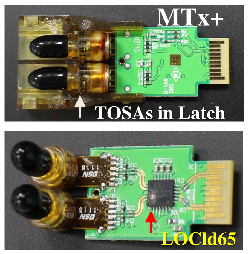
The MTx+ is developed in continuation of the MTx transmitter for applications in the ATLAS Phase-I upgrade [4]. The prototype MTx+ is designed with the circuit boards configured for plug-in to SFP+ connector, and the electrical inputs in CML (Current Mode Logic) protocol for high-speed interfacing. The differential signal swing is required for 100 mV minimum. The module assembly is customized to a total height of 6 mm, with a latch holding TOSAs and LC type fiber connectors for light coupling.
Illustrated in Fig. 1 is an earlier prototype module mounted on a test carrier board. The prototypes are also developed for the transceiver (MTRx+) with one transmitter (TX) channel assembled to the LOCld65. The receiver (RX) channel is a customized ROSA (Receiver Optical Sub Assembly) that has the Photo-Detector current collected by the GBTIA receiver chip [5] for output.
The prototype modules were first prepared with components specified for 10 Gbps including the TOSA, and the PCBs made of FR-4iii The FR-4 material is composed of fiber-glass reinforced epoxy-laminated sheets used in PCB manufacturing. material. The speed performance of the transmitter is measured for 14 Gbps, which is limited by the laboratory test facility.

The LOCld65 laser driver circuits developed for application in radiation field is required for the minimum speed of 10 Gbps and is configurable by an I2C interface. The schematic of the LOCld65 is plotted in Fig. 2. It has two separate channels of the same circuits and a slave I2C control section. The design goal is for each channel to amplify a differential signal of amplitude greater than 100 mV, and an 8 mA modulation current to a VCSEL.
Each of the LOCld65 channel consists of four functional blocks: an equalizer, four stages of limiting pre-amplifiers, a high-current output driver, and a bias-current generator. Each is programmable via the I2C interface. The I2C interface also provides an 1-bit register to turn the channel on or off independently.
The input of high-frequency signals is first compensated by the equalizer. It is then amplified and driven into an 8 mA modulation current to the external VCSEL, which is biased at 6 mA by the bias-current generator.
The equalizer is implemented taking into account the attenuation of high-frequency components of the input signals induced by non-ideal factors in devices such as the PCB traces, bonding wires, and ESD diodes. The equalizer design is a Continuous-Time Linear Equalizer with shunt peaking circuits to extend the bandwidth of input signals.
The pre-amplifier is required to output a large swing of up to 800 mV (peak to peak) to fully turn on/off the current driver which consists of an NMOS pair. A total gain of more than 18 dB is reached by designing the output driver with four stages of limiting amplifiers. The bandwidth is extended with shared inductors and feedback that can be adjusted by the I2C interface.
The current driver is optimized for output connected by a flex cable to a VCSEL in the TOSA package. The modulation of the VCSEL current is adjusted by a tail current source.
The post-layout simulation is conducted for each stage of the LOCld65, with the input amplitudes adjusted from the minimum required (100 mV) to higher values. The equalizer bandwidth can reach 32 GHz with a moderate R-C degeneration setting. An eye-diagram simulation for the current driver output is illustrated in Fig. 3, for the input signal of 25 Gbps and the amplitude of 200 mV. The eye-diagrams are compared for different input amplitudes. The results are compatible for the amplitudes of 100 mV and up to 1 V.


3 Revision of the MTx+ for 25 Gbps
The bandwidth of the initial version of MTx+ has exceeded the expected 10 Gbps speed. It is investigated further for higher bandwidth with the circuit design and components revised for 25 Gbps. The PCB material is replaced by the Panasonic MEGTRON6 [6]. The circuit layout is modified and the cabling for electrical input signals are all upgraded accordingly.
The module assembly has used two types of VCSELs in TOSA packages, the 10 Gbps rated TOSA of Truelight [7] and the 25 Gbps TOSA of SAN-U [8]. Illustrated in Fig. 4 are pictures of the new MTx+ modules. The test setup with the MTx+ mounted on a test carrier board is shown in Fig. 5. The electrical input waveforms are generated by an Anritsu MP1800A signal analyzer with the amplitude set to 1 V. The eye-diagrams are measured by a Keysight DCA-X 86100D oscilloscope. For this test, input signals are tuned from 10 Gbps to 25 Gbps in steps. We optimize the operation of the LOCld65 equalizer receiving the input signals, as well as the bias and modulation to the VCSELs, through the I2C interface. The same configuration is applied for all measurements at different speeds.
Shown in Fig. 6 is a typical eye-diagram measured at 25 Gbps for a MTx+ channel assembled with a SAN-U TOSA. This type of TOSA has a large light power. The measured value is 1.25 dBm. The rise and fall time of the eye-diagram are about 30 ps at 10 % and 90 % of the step height, respectively, and the RMS jitter is 2 ps. The gray area in the eye-diagram is the 25 Gbps mask. The mask margin obtained is 22 %.
We have compared this previous measurement to the MTx+ using a slower 10 Gbps TOSA (of Truelight). The bandwidth is limited by the TOSA and the test has achieved a data transmission rate of 20 Gbps. The eye-diagram is shown in Fig. 7. This confirms that the LOCld65 and the PCB assembly are all qualified for speed performance higher than 20 Gbps.

4 Summary
The dual-channel MTx+ transmitter consists of the LOCld65 laser driver and 850 nm VCSELs in TOSA packages. The speed performance is investigated with the modules made of PCB material and components qualified for 25 Gbps applications. The eye-diagram observed for data transmission at 25 Gbps has a mask margin measured to be 22 %. The revised MTx+ has reached the speed performance of 25 Gbps being pursued.
References
- [1] “Radiation hardness of optoelectronic components for the optical readout of the ATLAS inner detector”, S. Hou, et al., Nucl. Instr. and Meth. A 636 (2011) S137.
- [2] “LOCld65, A Dual-Channel VCSEL Driver ASIC For Detector Front-End Readout”, W. Zhou, et al., IEEE Trans Nucl. Sci., 66 (2019) 1115.
- [3] “A TOSA/ROSA-based optical transmitter (MTx+)/transceiver (MTRx+) for high-energy physics experiments”, B. Deng et al., JINST 14 (2019) C05021.
- [4] “Mid-board miniature dual channel optical transmitter MTx and transceiver MTRx”, X. Zhao et al., JINST 11 (2016) C03054.
- [5] “The GBTIA, a 5 Gbit/s Radiation-Hard Optical Receiver for the SLHC Upgrades”, M. Menouni et al., in proceedings of TWEPP-09, CERN-2009-006, (2009).
- [6] MEGTRON6 of the Panasonic Corp.; high speed, low Loss multi-layer materials.
- [7] TTR-1F59 of the Truelight Corp.; 10 Gbps LC connectorized 850nm VCSEL.
- [8] 4020121000 of the SAN-U Optronics; TOSA-LC 25 Gbps with AFCD-V51KC-DS of the Avago Technologies.