Polarized Raman Analysis at Low Temperature to Examine Interface Phonons in Quantum Dot Heterostructures
Abstract
An experimental study of optical phonon modes, both normal and interface (IF) phonons, in bilayer strain-coupled quantum dot heterostructures has been presented by means of low-temperature polarized Raman scattering. The effect of -content on the frequency positions of these phonon modes has been very well correlated with the simulated strain. The Raman peaks show different frequency shifts in the heterostructure with varying -content in the capping layer. This shift is attributed to the strain relaxation, bigger size of quantum dots and type-II band alignment.
I Introduction
Self-assembled based quantum dot (QD) devices have garnered significant attention from the research community due to their potential for use in a broad spectrum of optoelectronic applications. These self-assembled QDs offer the advantage of creating defect-free systems that confine charge carriers within nanometer-scale dimensions without the need for complex lithography and etching processes. These QDs are usually produced by the Stranski-Krastanov process during the growth of mismatched materials using molecular beam epitaxy (MBE). In this process, interlayer strain is essential in creating pyramid-shaped or hemispherical dots on a thin wetting layer. The strain-coupling in these self-assembled QD systems is particularly advantageous as it facilitates the vertical ordering of QDs in multilayer QD systems. This vertical alignment increases the volume of active regions, thereby enhancing absorption efficiency. Tutu et al. (2012); Kim et al. (2004); Panda et al. (2018) Moreover, the linewidth of photoluminescence (PL) spectra and the uniformity in dot size can be precisely controlled, making these systems highly desirable for various applications. Panda et al. (2017) Specifically, this strain-coupling effect has been effectively utilized in QD systems to achive an emission wavelength of , which is highly relevant for telecommunications applications. Dowd et al. (1999); Ledentsov et al. (2002) Given the significance of these strain-coupled heterostructures, they have become a focal point of research in device applications, particularly in the telecommunications sector. However, there is ongoing research to push the emission wavelength beyond to meet the increasing demands of advanced telecommunications technologies. One promising approach to achieving this is the incorporation of into the the system, where is used as a capping layer in QD systems. This modification increases the aspect ratio of the QDs, thereby reducing the strain within them and leads to a redshift of the emission wavelength. The QD systems have gained popularity due to the intriguing properties that arise from varying the composition. Notably, it has been observed that the band alignment in these systems shifts from type-I to type-II beyond a certain -composition (approximately ).Ulloa et al. (2012); Ripalda et al. (2005); Jang et al. (2008) This unique property allows QDs to facilitates emission wavelength beyond , which is particularly valuable for advanced telecommunications. Akahane et al. (2006) For instance, recent work by Saha et alSaha et al. (2019) reported a room temperature emission at approximately from the strain-coupled bilayer QD heterostructures, further highlighting the potential of these systems for next-generation optoelectronic devices.
The generation of quantum dots (QDs) is heavily dependent on strain, which has important ramifications for QD applications in various devices. Understanding how strain affects the electronic, vibrational, and optical properties of QDs is therefore essential. Numerous studies have been conducted to explore the impact of strain on the electronic and vibrational (phonon) structures of QDs using techniques such as X-ray diffraction, Raman spectroscopy, photoluminescence (PL), and photoluminescence excitation spectroscopy. Phonons are essential to electron-phonon scattering, which affects the carrier relaxation process, which is a crucial element in determining the performance of semiconductor devices. For this reason, the study of phonon characteristics is especially relevant to device applications. Raman spectroscopy is an effective tool for investigating phonon modes, as it provides valuable insights into doping levels, crystalline quality, impurity concentrations, and other material characteristics. Despite its advantages, the study of phonon properties in strained QD systems using Raman spectroscopy has been limited. This is primarily because the Raman signals from QDs are often weak due to the small scattering volume of the QDs compared to the surrounding capping material and substrate. Additionally, self-assembled QDs typically exhibit strongly corrugated interfaces, which can lead to the emergence of IF phonon modes that are localized at the tips and cusps of the QDs, as predicted by Knipp and ReineckeKnipp and Reinecke (1992) using the dielectric continuum model. There have been several studies focusing on the IF phonon modes in QDs, utilizing techniques such as PL and both normal and resonance Raman spectroscopy. These studies have successfully identified various IF modes and examined their behavior in response to different growth parameters. For example, Puesp et alPusep et al. (1998) reported the presence of IF modes localized near the edges of the QDs in and in () structures. In further research, Puesp et alPusep et al. (1998) used resonance Raman scattering at the gaps of and to identify distinct IF modes and demonstrated a strong influence of strain on these modes. These findings underscore the importance of studying phonon properties in strained QD systems, as they provide critical insights about how strain affects the electronic and vibrational properties of the material.
Despite the significant interest in the optical and electronic properties of / quantum dot (QD) systems, there has been a noticeable lack of studies focusing on the normal and IF phonon modes in these structures. The work by Dai et alDai et al. (2015) represents one of the few exceptions, where they examined QDs capped with using an spray technique applied immediately prior to capping. Their research highlighted changes in photoluminescence (PL) emission intensity and a redshift in emission wavelength corresponding to different durations of spray. However, the weak signals obtained in their study limited the unambiguous identification of distinct phonon modes. Dai et alDai et al. (2015) concluded that the spray likely reduced defects and contributed to strain relaxation by facilitating the formation of at the QD/cap interface. In this paper, we address this gap by presenting the results and analysis of our low-temperature polarized Raman measurements aimed at investigating the frequency positions of both normal and IF phonons in bilayer QDs heterostructures. Our study seeks to provide a clearer understanding of the phonon modes in these strained systems, which is critical for advancing the development of QD-based optoelectronic devices.
II Experimental details
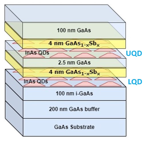
Strain-coupled bilayer QDs were grown by the MBE system via Stransky-Krastanov growth. Fig. 1 illustrates the schematic representation of the developed heterostructure, featuring two layers of QDs capped with a capping layer. The bilayer QD architecture is characterized by strain coupling with a spacer, wherein the lower QD possesses a coverage, while the upper QD (UQD) has a 3.2 ML coverage. Consequently, the UQD exhibits larger dimensions compared to the lower QD (LQD), as evidenced by a Transmission Electron Microscopy (TEM) image as shown in Fig. 2. The two dot layers are separated by a spacer layer of and capped with capping material. The -composition has been taken as % and % in the capping material and referred as samples A and B, respectively. The details of the growth have been mentioned in our previous study. Saha et al. (2019)


A frequency doubled Nd:Yag laser focused on a spot with of power at the laser head was used to excite the Raman spectra. Spectra were collected in backscattering geometry and analyzed using an HR800-UV confocal micro-Raman spectrometer. The measurements were acquired in and polarization with and . Samples were cooled to to reduce the width of the different Raman lines so that the very weak IF phonon modes could be observed in the presence of comparatively stronger normal phonon modes. The heterostructures were simulated by Nextnano softwareBirner et al. (2007) to visualize the distribution of strain field in the different layers and dimensions of QD were taken according to the TEM image shown in Fig. 2. This software comprises a complete database of group III-V materials’ characteristics and allows for 3-dimensional simulations of the quantum mechanical electronic structure within the heterostructure. We have already mentioned the software related details in our previous work by Saha et al.Saha et al. (2019)
Fig. 3 shows the contour of the strain field in both samples, wherein both QDs are under tensile strain. Generally, tensile strain is positive, and compressive strain is negative in magnitude. The strain is compressive at the bottom of LQD, tensile inside the QD region, compressive towards the capping layers, and finally tensile at the end of the capping layer of UQD. This can be attributed to the larger lattice constant of InAs compared to GaAs. Additionally, it can be observed that the strain field is different at the center and the edge of QD. Two cutlines, cutline ( and ) and cutline ( and ), are marked at the center and edge of QD respectively, and these markings are used to analyze strain later in the manuscript. The magnitude of strain in sample B is lower as compared to sample A. This is due to the bigger size of QDsSaha et al. (2019) and the presence of high -composition in the capping layer of sample B, which reduces the lattice mismatch between the InAs QDs and capping layer, and thereby decreasing the strain within the entire heterostructure.
III Theoretical Analysis

In order to assign the different phonon modes, it is necessary to analyze and estimate quantitatively the effects of strain on different phonon modes. As shown by the simulation of strain profiles in both the samples, both UQD and LQD are under considerable strain and it is known that the phonon mode frequencies exhibit both blue-shift as well as red-shift, by compressive and tensile strains. Thus, it is necessary to estimate the strain profiles over the QD heterostructures to provide explanation for the origin of the different Raman lines in both samples. Cardeira et al Cerdeira et al. (1972) have carried out a detailed examination of stress-induced Raman mode shifts in various zinc-blende and diamond semiconductors and we use their framework to estimate the position of different phonon modes. The strain tensor components can be broadly expressed as hydrostatic and biaxial strain denoted by and respectively. These are defined asXiong and Zhang (2017)
| (1) |
| (2) |
Where, is the diagonal components of the strain tensor. Fig. 4 (a) and (b) for samples A and B, respectively, at both cutlines, display the simulated strain components. The and strain profiles are similar (compressive), as the definition of material layers are the same in the both x and y directions, whereas the strain is tensile in the z-direction. The changes in the phonon frequencies for the transverse optical modes () and longitudinal optical mode () can be calculated following the prescription outlined by Cardeira et alCerdeira et al. (1972) where they have shown that the application of uniaxial stress causes a shift of the phonon, while the mode shows both a splitting and shift. They had further shown that the shifts can be expressed as due to hydrostatic and biaxial stain ( and respectively ) and can be calculated in terms of the material properties , , and which outline the modifications to the “spring constants” of the optical phonons. These parameters have been listed by Cardeira et alCerdeira et al. (1972) for a set of III- V semiconductors. The unperturbed phonons are denoted by and the shifted ones are by respectively. The frequency shift of the and modes as a function of hydrostatic and biaxial strain along the growth direction of the QD heterostructures can be used to calculate and interpret the various observed lines in the Raman spectra for the two samples (discussed in next section). We note here that exhibits two mode behavior with like and like modes with like modes are most intenseYano et al. (1989). For , the like mode for is more or less the same as that for and the modeYano et al. (1989) is at . However, for , we use phonon modeYano et al. (1989) at and for phonon . The frequencies of , , and layers in the lower and upper QDs and the capping layers have been calculated and can be Visualized in terms of depth. It is evident that the strain profile is slightly different at the center ( and ) and at the edge ( and ) and the Raman frequencies have also been calculated for these positions. Fig. 4 (c) and (d) show and for both of the samples A and B respectively Corresponding to growth direction covering both the UQD and LQD. It can seen that the variation of both and over LQD and UQD at the center of QD ( and ) and edge of QD ( and ) are quite different for both of the samples. In particular, over LQD has a sharp spike while its variation over UQD is more gradual. Using Eqs. 39 and 42 from MS thesis of HusseyHussey (2007) and / strain distribution we can determine the phonon shift for the and modes, as shown in Fig. 5. The figure depicts the shift in and phonon modes in the UQD region for both samples. It is mainly because most of the Raman signal originates from top . Since modes are usually stronger compared to modes we concentrate on Fig. 5 (c) and (d). The phonon over most of the region around the center of QD ( and ) is with a sharp downward spike at edge of QD ( and ). This is to be mentioned here that there are different expressions for the biaxial strain as a function of different strain components used by different authors.
| (3) |
| (4) |
To compare the magnitude of shifts obtained using the different expressions, we have also performed calculations using two other expressions ( Eqs. (3)Cusack, Briddon, and Jaros (1996) and Eqs. (LABEL:eq:four)Grundmann, Stier, and Bimberg (1995)) for biaxial strains. However, we observe that the changes are very small and it can be attributed to the fact that the biaxial strain for these materials (, , ) is much smaller compared to that for hydrostatic strain.
IV Experimental Results
The Raman selection criteria for backscattering geometry for type substrates predicts allowed and forbidden for geometry and and both forbidden for geometry. Fig. 6 (a) and (b) exhibit the Raman spectra acquired in geometry for samples A and B. It can be seen that only two distinct peaks are visible, which are attributed to () and () phonons at and respectively. This is expected since the penetration depth of laser line for GaAs is and most of the signal arises from the top capping layer and the UQD with capping layer, however, the contribution of the Raman signals arising from the LQD and layers is relatively poorer. Further, it has been earlier reported that the and like IF modes appear close to peak positions and are very small in intensityPusep et al. (1998), and thus the geometry is suitable to minimize the contributions for both the and modes. It is known that the Raman linewidth reduces with decreasing temperature, parallel polarized Raman measurements in the later geometry were recorded at to visualize different peaks originating from the corrugated interfaces of , , and . Fig. 6 (c) and (d) show low temperature () Raman spectra of both the samples measured in scattering geometry and they were best fitted with five Lorentzian curves. The highest intensity peaks, peak 3 and peak 5 correspond to (, and ( phonon modes respectively. The other peaks correspond to QDs and , capping layer phonon modes. Also, the Raman peaks have a broad asymmetrical feature around (peak ) and (peak ). These modes are at slightly different frequency positions for both samples. The frequency positions are right-shifted to higher energy in sample B ( -content) as compared to sample A (having -content). The higher content in sample B reduces the strain over the entire heterostructure (as earlier observed in the simulated strain profiles), which results in shift of the peak positions from their bulk value. The frequencies of and phonons in bulk are and , respectivelyPusep et al. (1998), whereas we observe two peaks at and in samples A and B respectively. These peak positions are at much higher frequencies than the modes but considerably lower than those for . The origin of these modes can be explained using our theoretical analysis for uniaxial and biaxial stress-induced shift of the optical phonon modes in QDs using the method outlined in the previous section (Theoretical Analysis) for both samples A and B. Fig. 5 (c) and (d) show that the phonon modes are shifted to higher frequency , which is attributed to the compressive hydrostatic and tensile biaxial strain. Thus, we assign these modes (peak 2) as peaks. This agrees with the results reported by other authors. Raman spectroscopic study by Puesp et alPusep et al. (1998) on self-assembled QDs have observed the QD LO mode at which agrees very well with our value. Similarly, Milekhin et alMilekhin et al. (2004a) also assigned a value of for this mode.

In addition to the strong and modes of (peaks and ) and QD mode( peak ), there are additional weak shoulder peaks present at lower frequency side of phonons (peak and peak ) which cannot be assigned to optical phonons. We ascribe them to be IF modes between the QD in and matrix. The frequency positions of the -like IF peak are at (peak 4) in both the samples. This peak position is right shifted towards higher energy from the earlier reportedMilekhin et al. (2004b) position of because of the inclusion of composition in the capping layer which causes strain relaxation in the heterostructureMilekhin et al. (2004b) with shift towards the bulk value. Another distinct peak at (peak ) is attributed to the IF mode of QD like mode. This peak is at position and in samples A and B, respectively. Furthermore, the Full Width Half Maximum (FWHM) of most of the peaks (peak , and ) is larger in sample B as compared to sample A. This might be due to the higher -composition in the capping layer, which causes the localization of electrons in one material ( QDs) and holes in another material ( capping region), thereby transforming the band alignment to be of type-II nature. However, all the peak positions in sample B are right-shifted by more than , which is due to the bigger dot size and better strain relaxation inside the heterostructure (as discussed earlier). Dai et alDai et al. (2015) had attributed a mode at alloy mode with longest spray time, which we don’t observe due to poor S/N value over . However a Raman study of with varying (Yano et alYano et al. (1989) ) indicates that it can be assigned as pure mode. In addition, they assign as QD mode while we observe the QD mode at . We can estimate the frequency of the IF modes by following the prescription by Knipp and ReineckeKnipp and Reinecke (1992) based on the classical continuum dielectric approach without retardation, whereby the IF mode frequencies fall with the non-overlapping regions of the dot and the barrier materials. This is valid for QDs in barrier and assuming the QDs as ellipsoidal shapes with height and width obtained from the cross-sectional TEM. We calculate the IF frequencies by following the code given by HussayHussey (2007) using Mathematica. The calculated frequencies for l=1-3 are shown in Table 1. According to the calculation, the first IF mode (peak 4) matches well with l=3 and m=0 in both samples, while IF mode with and is closer to the strong mode. Thus, peak and peak are assigned as -like IF and -like IF modes respectively.
| Sample | |||
|---|---|---|---|
| A | |||
| B | |||
V Conclusion
In conclusion, we have identified distinct Raman peaks in the QD heterostructures. The phonon modes exhibited a shift to higher frequencies due to the increased -composition in the capping layer. Additionally, the FWHM of the peaks was broader, indicating increased disorder and type-II band alignment. The QD heterostructure with a capping layer demonstrated a reduced strain profile, attributed to the lower lattice mismatch between QDs and the capping material. This reduction in strain led to larger quantum dots and resulted in longer wavelength emission. All observed modes have been assigned to the highly strained mode of the QD and the and modes of . Additionally, we have identified two IF modes, which we have assigned as -like and -like IF modes.
Acknowledgements.
Financial support was provided by the Indian Institute of Technology Gandhinagar under grant number IP/ITGN/EE/JS/2122/08. The authors acknowledge Baolai Liang of UCLA for the growth of the samples and Sophisticated Analytical Instrument Facility) SAIF, IIT Bombay.References
- Tutu et al. (2012) F. Tutu, I. Sellers, M. Peinado, C. Pastore, S. Willis, A. Watt, T. Wang, and H. Liu, “Improved performance of multilayer quantum-dot solar cells using a high-growth-temperature spacer layer,” Journal of Applied Physics 111 (2012).
- Kim et al. (2004) E.-T. Kim, A. Madhukar, Z. Ye, and J. C. Campbell, “High detectivity quantum dot infrared photodetectors,” Applied Physics Letters 84, 3277–3279 (2004).
- Panda et al. (2018) D. Panda, J. Saha, A. Balgarkashi, S. Shetty, H. Rawool, S. M. Singh, S. Upadhyay, B. Tongbram, and S. Chakrabarti, “Optimization of dot layer periodicity through analysis of strain and electronic profile in vertically stacked quantum dot heterostructure,” Journal of Alloys and Compounds 736, 216–224 (2018).
- Panda et al. (2017) D. Panda, A. Ahmad, H. Ghadi, S. Adhikary, B. Tongbram, and S. Chakrabarti, “Evidence of quantum dot size uniformity in strain-coupled multilayered QDs grown with constant overgrowth percentage,” Journal of Luminescence 192, 562–566 (2017).
- Dowd et al. (1999) P. Dowd, W. Braun, C. Ryu, C.-Z. Guo, S. Chen, U. Koelle, S. Johnson, Y.-H. Zhang, and D. Smith, “1.3 m light emitting diode grown on ,” in Conference on Lasers and Electro-Optics (Optica Publishing Group, 1999) p. CThV5.
- Ledentsov et al. (2002) N. N. Ledentsov, V. M. Ustinov, D. Bimberg, J. A. Lott, and Z. I. Alferov, “Applications of quantum dots in semiconductor lasers,” International journal of high speed electronics and systems 12, 177–205 (2002).
- Ulloa et al. (2012) J. Ulloa, J. Llorens, M. Del Moral, M. Bozkurt, P. Koenraad, and A. Hierro, “Analysis of the modified optical properties and band structure of -capped quantum dots,” Journal of Applied Physics 112 (2012).
- Ripalda et al. (2005) J. M. Ripalda, D. Granados, Y. González, A. Sánchez, S. I. Molina, and J. García, “Room temperature emission at 1.6 m from quantum dots capped with ,” Applied Physics Letters 87 (2005).
- Jang et al. (2008) Y. Jang, T. Badcock, D. Mowbray, M. Skolnick, J. Park, D. Lee, H. Liu, M. Steer, and M. Hopkinson, “Carrier lifetimes in type-ii quantum dots capped with a strain reducing layer,” Applied Physics Letters 92 (2008).
- Akahane et al. (2006) K. Akahane, N. Yamamoto, S.-i. Gozu, A. Ueta, and N. Ohtani, “1.5 m emission from quantum dots with strain-reducing layer grown on substrates,” Physica E: Low-dimensional Systems and Nanostructures 32, 81–84 (2006).
- Saha et al. (2019) J. Saha, D. Das, D. Panda, B. Tongbram, A. Chatterjee, B. Liang, K. D. Gupta, S. K. Pal, and S. Chakrabarti, “Broad tunability of emission wavelength by strain coupled quantum dot heterostructures,” Journal of Applied Physics 126 (2019).
- Knipp and Reinecke (1992) P. Knipp and T. Reinecke, “Classical interface modes of quantum dots,” Physical Review B 46, 10310 (1992).
- Pusep et al. (1998) Y. A. Pusep, G. Zanelatto, S. Da Silva, J. Galzerani, P. P. González-Borrero, A. Toropov, and P. Basmaji, “Raman study of interface modes subjected to strain in self-assembled quantum dots,” Physical Review B 58, R1770 (1998).
- Dai et al. (2015) L. Dai, S. P. Bremner, S. Tan, S. Wang, G. Zhang, and Z. Liu, “Raman scattering study on Sb spray quantum dot nanostructure systems,” Nanoscale research letters 10, 1–6 (2015).
- Birner et al. (2007) S. Birner, T. Zibold, T. Andlauer, T. Kubis, M. Sabathil, A. Trellakis, and P. Vogl, “Nextnano: general purpose 3-d simulations,” IEEE Transactions on Electron Devices 54, 2137–2142 (2007).
- Cerdeira et al. (1972) F. Cerdeira, C. Buchenauer, F. H. Pollak, and M. Cardona, “Stress-induced shifts of first-order raman frequencies of diamond-and zinc-blende-type semiconductors,” Physical Review B 5, 580 (1972).
- Xiong and Zhang (2017) Y. Xiong and X. Zhang, “An accurate method of modeling self-assembled (001) quantum dot with double-capping procedure,” IEEE Journal of Quantum Electronics 53, 1–11 (2017).
- Yano et al. (1989) M. Yano, M. Ashida, A. Kawaguchi, Y. Iwai, and M. Inoue, “Molecular-beam epitaxial growth and interface characteristics of on substrates,” Journal of Vacuum Science & Technology B: Microelectronics Processing and Phenomena 7, 199–203 (1989).
- Hussey (2007) L. K. Hussey, “Raman spectroscopy of quantum dots patterned by nano-indentation,” MS thesis, College of Arts and Sciences, University of South Florida (2007).
- Cusack, Briddon, and Jaros (1996) M. Cusack, P. Briddon, and M. a. Jaros, “Electronic structure of self-assembled quantum dots,” Physical Review B 54, R2300 (1996).
- Grundmann, Stier, and Bimberg (1995) M. Grundmann, O. Stier, and D. Bimberg, “ pyramidal quantum dots: Strain distribution, optical phonons, and electronic structure,” Physical Review B 52, 11969 (1995).
- Milekhin et al. (2004a) A. G. Milekhin, D. A. Tenne, A. I. Toropov, A. K. Bakarov, S. Schulze, and D. R. Zahn, “Raman study of interface phonons in quantum dot structures,” physica status solidi (c) 1, 2629–2633 (2004a).
- Milekhin et al. (2004b) A. Milekhin, A. Toropov, A. Bakarov, D. Tenne, G. Zanelatto, J. Galzerani, S. Schulze, and D. Zahn, “Interface phonons in and quantum dot structures,” Physical Review B 70, 085314 (2004b).