Piezoelectric Electrostatic Superlattices in Monolayer MoS2
Abstract
Modulation of electronic properties of materials by electric fields is central to the operation of modern semiconductor devices, providing access to complex electronic behaviors and greater freedom in tuning the energy bands of materials. Here, we explore one-dimensional superlattices induced by a confining electrostatic potential in monolayer MoS2, a prototypical two-dimensional semiconductor. Using first-principles calculations, we show that periodic potentials applied to monolayer MoS2 induce electrostatic superlattices in which the response is dominated by structural distortions relative to purely electronic effects. These structural distortions reduce the intrinsic band gap of the monolayer substantially while also polarizing the monolayer through piezoelectric coupling, resulting in spatial separation of charge carriers as well as Stark shifts that produce dispersive minibands. Importantly, these minibands inherit the valley-selective magnetic properties of monolayer MoS2, enabling fine control over spin-valley coupling in MoS2 and similar transition-metal dichalcogenides.
I Introduction
The electronic band structure of a solid—a representation of allowed electronic energy levels—reflects the quantum mechanical response of electrons to the underlying periodic potential of the atomic lattice. A superlattice induces further periodic modulations of the lattice potential over length scales several times larger than the atomic spacing yet smaller than the mean free path of an electron, localizing free carriers and causing further quantization of energy bands into minibands. [1, 2] While semiconductor superlattices are typically produced by alternating layers of different semiconductors or by differently doped (n-/p-type) layers of a single semiconductor, it is also possible to induce directly a superlattice potential via externally defined electrostatic gates or patterned dielectric substrates.[3, 4, 5, 6, 7, 8] Such externally-defined electrostatic superlattices (henceforth, simply “electrostatic superlatttices”), employed early on with two-dimensional (2D) electron gases, [9, 10, 11] continue to attract interest in 2D materials, [3, 4, 5, 6, 7, 8, 12] motivated in part by theoretical studies of 2D superlattices that promise key advances, for example, in supercollimation, Mott-insulating states, superconductivity, and topological subbands.[13, 14, 15, 16, 17, 18] It is worth noting that superlattices in 2D materials can also be achieved by various other means, for example, by exploiting the naturally occurring periodic potential of Moiré patterns [19, 20, 21, 22] or via strain patterning, [23, 24, 25] among others. An assessment of these various approaches can be found in a recent review.[8]
To date, studies of 2D electrostatic superlattices—either experimental [3, 4, 5, 6, 7, 8, 12] or theoretical [13, 26, 27, 28, 29, 30, 31]—have focused primarily on graphene (a semi-metal). In comparison, electrostatic superlattices in 2D transition-metal dichalcogenides (TMDCs) are sparsely studied, that too only at the theoretical level [32, 33] without accounting for the role of potential-induced strains. However, not only is it well known that the (opto)electronic properties of TMDCs are sensitive to strain [34, 35, 36, 37] but it is also well known that inhomogeneous strains can lead to spatial variations in band profiles that cause, for example, funneling of excitons and trions. [23, 38, 39, 40] In contrast, this coupling between strain and potential has been studied widely in Moiré superlattices of TMDCs (homo-/hetero-bilayers) and it is recognized that accounting for spatial variations of strain and morphology is essential for modeling the response of these structures correctly.[41, 42, 43, 44, 45] Thus, in this paper, we take a prototypical example of a one-dimensional (1D) electronic superlattice in monolayer MoS2 and seek to understand how coupling between the external electrostatic potential and induced strains affects the electronic response of the material. We employ first-principles density functional theory calculations and show that significant atomic relaxation is possible within the MoS2 monolayer, when subjected to a periodic external potential, and that these effects can lead to over an order of magnitude decrease in the superlattice band gap than would be anticipated from a purely electronic response. Moreover, since monolayer MoS2 is piezoelectric,[46] we find a strong anisotropic, spatially-varying coupling of the polarization response to the strain field induced by the external superlattice potential, and we show that the internal polarization fields significantly influence mini-band formation. Importantly, we find that the mini-bands formed at the band edges preserve the appealing spin–valley coupling property of monolayer MoS2, opening up possibilities for spin-selective mini-band engineering of MoS2 and analogous 2D semiconductors.
II Results and Discussion
The key concept of this paper is illustrated schematically in Fig.1: we seek to understand the response of a 2D semiconductor (e.g., monolayer MoS2) subjected to a spatially-periodic potential, , whose magnitude is much smaller than the potential of the nuclei. If we ignore the forces induced by the applied potential on the atoms, the response of the material is purely electronic, and the energy levels rise and fall in phase with the potential modulation (Fig.1B). As a consequence, the valence band maximum (VBM) and the conduction band minimum (CBM) are localized at the corresponding maximum and minimum of the applied potential and are spatially separated. In analogy with the more familiar situation of semiconductor heterojunctions, the material response is akin to a staggered-gap (type II) heterojunction. [9] However, if structural relaxation is accounted for, as it should be, atoms are displaced from regions of higher potential energy towards regions of lower potential energy, leading to a distribution of tensile and compressive strains within the material (Fig.1C). It is well known that the electronic structures of 2D materials are sensitive to strain[34]: in the case of monolayer MoS2, the band gap decreases or increases under tension and compression, respectively. [36, 35] Thus, the shifts in electronic energies are no longer merely in phase with the applied potential and, depending upon the precise balance between strain- and potential-induced effects, the VBM and CBM can instead localize within the same region of high tensile strain where the band gap is smallest. This scenario is now akin to a straddling-gap (type I) heterojunction. It is precisely this coupling between external fields and induced strains, and the ultimate consequences for the electronic response of the monolayer, that we explore in detail here. Additionally, for a material such as MoS2, the electronic response is much richer due to its intrinsic piezoelectricity [46, 47] and spin–valley coupling, [48, 49] which we explore in detail below.

II.1 Electric field-induced piezoelectric coupling
In this work, we restrict attention to one-dimensional potential modulations, , with the vector directed along either the armchair or the zigzag direction: Figure 2A displays an example of a superlattice along the armchair direction with =0.1 V and period =17.6 nm. The functional form of this potential is motivated by the calculated displacement fields in Ref. 3 and we assume that the field does not vary appreciably across the thickness of the monolayer. In response to this external perturbation, atoms are displaced from regions of higher potential towards regions of lower potential (peak displacement of Å; Fig. 2C), leading to tensile and compressive strains, , that range between (Fig. S2). Figure 2B displays the spatial distribution of band edges from which we observe that electronic states, as deep as 0.1-0.2 eV into the valence or conduction band, are predominantly localized within the region of tensile strain. The perturbation reduces the overall band gap by relative to the unperturbed bandgap of monolayer MoS2 (from 1.67 eV to 1.13 eV). By comparison, if atoms are held fixed at their original positions (no structural relaxation; Fig. S3), the valence and conduction band edges are spatially separated, localizing within regions of positive and negative potential, respectively, that too becoming more distinct only at larger fields. The decrease in the band gap is now less than 1% ( meV), over an order of magnitude smaller than the relaxed case at the same applied potential. These observations essentially confirm, at least to lowest order, the simple physical picture presented previously. Of course, the armchair direction is not special in this regard, and a calculation for a cosine potential applied along the zigzag direction shows analogous atomic displacements and localization of band edges within the region of tensile strain, (Fig. S4). However, there is one crucial distinction between the responses of the armchair and zigzag directions: for the armchair case, the VBM and CBM, though localized within the region of tensile strain, have very little spatial overlap (Fig. 2B); in contrast, for the zigzag case, the VBM and CBM overlap spatially within the region of tensile strain (Fig. S4). To understand this markedly anisotropic response, we undertake a more detailed analysis of the structural response in each case.
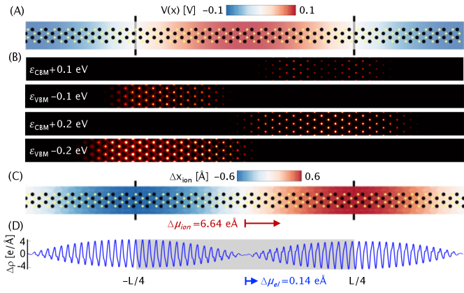
Monolayer MoS2 (space group ; point group ) lacks a center of inversion and is strongly piezoelectric. [46] The polarization vector () and strain tensor () are related via the constitutive relation , where is the third-rank piezoelectric tensor. [50] When the external potential is aligned with the armchair direction (), the piezoelectric coupling to the induced strain field induces a polarization field that is aligned with the armchair direction (). In contrast, when the external potential is aligned with the zigzag direction (), the polarization field is along the orthogonal armchair direction (). Further details can be found in the supplementary text. 111See Supplemental Material at [URL will be inserted by publisher] for details. Considering the armchair case and focusing on the region of tensile strain where the band edges are localized, we calculate a net ionic dipole moment of 6.64 eÅ or along the direction of quantization (). 222The areal dimensions of the supercell are 176.41 Å 3.18 Å while the thickness of the monolayer is 3.13 Å. Note that this degree of polarization is comparable to the remnant polarization in several ferroelectric materials. [53] Thus, separation of the valence and conduction band edges within the tensile region is driven by the internal electric field that arises from piezoelectric coupling to the strain field induced by the external potential. For a larger external potential (=0.3 V; Fig. S5), both the localization of band edges within the region of tensile strain as well as their spatial separation are more marked, as deep as 0.5 eV into the valence/conduction band. By contrast, for the zigzag case, the dipole moments within the region of tensile strain are orthogonal to the direction of quantization and, hence, there is no further spatial separation of band edges within this region of quantum confinement.
II.2 Minibands and band-gap tuning

We now investigate the influence of structural relaxation and strain-induced internal electric fields on the electronic bandstructure of monolayer MoS2 and the emergence of superlattice minibands. As the external potential and structural relaxation can be viewed as perturbations to the pristine MoS2 monolayer, unfolding the superlattice bandstructure [54, 55, 56] from its reduced Brillouin zone to the full (extended) Brillouin zone of monolayer MoS2 (Appendix B; Fig. 6) allows for a more transparent analysis. Figures 3(A, B) display the unfolded bandstructures for the unrelaxed and relaxed armchair superlattices, from which we note several important distinctions. In the unrelaxed case (Fig. 3A), the change in band gap is small (; 15 meV) for this magnitude of external potential (=0.1V), and the gap remains direct at the K valleys. In the extended zone picture, we clearly observe the formation of superlattice minibands that are gapped due to the quantum confinement effect of the external potential. When the lattice is allowed to relax, these gapped minibands are further dispersed and the decrease in band gap is more substantial (; 0.54 eV for =0.1 V), the gap now being indirect between the valley at the valence band edge and the (degenerate) K valleys at the conduction band edge; the direct gap at the K valleys is meV larger. Similar results are seen in the zigzag case (Fig. S6). For a larger external potential (=0.3 V; Fig. S7), the miniband dispersion becomes even more distinct with substantial miniband gaps (tens of meV). To demonstrate conclusively the structural basis of our findings, we recalculated the bandstructures of fully relaxed superlattices by artificially fixing atoms at their (field-dependent) positions and turning off the external potential (Figs. S8, S9) and found relatively small changes () in the band gap with no qualitative changes in the miniband dispersion. We therefore conclude that the miniband dispersion occurs primarily due to Stark shifts driven by the internal polarization field that arises from piezoelectric coupling to the induced strain in the superlattice. Such effects are well known in quantum wells heterostructures composed of piezoelectric materials (e.g., zincblende-structure III-V superlattices [2]) in which strains at interfaces produce built-in electric fields that lead to Stark shifts and consequent dispersion of minibands that are accompanied by a decrease in the band gap. The important distinction is that, unlike quantum-well heterostructures involving dissimilar materials, we have here an electrostatic superlattice in a pristine monolayer of a single-phase 2D material that displays analogous physics.

To complete our analysis of bandgap tuning of monolayer MoS2 electrostatic superlattices, we sampled the parameter space of such superlattices, including wavelengths and amplitudes of potential modulations as well as the effects of structural relaxation. The outcome of these studies is displayed in Figure 4, from which we see that: (i) for a given superlattice length, , the band gap, , decreases nearly linearly with the amplitude, , of the applied potential; [32] (ii) for a fixed value of , a longer supercell experiences a greater reduction in band gap; and (iii) the reduction in band gap is substantially greater when structural relaxation is allowed. These observations hold irrespective of the direction – armchair or zigzag – of the potential modulation. Based on these observations, we make a scaling ansatz
| (1) |
where is the band gap of an unperturbed MoS2 monolayer, is the lattice constant of the monolayer, is the elementary charge, and and are fitting parameters. Given the vast difference in behavior between unrelaxed and relaxed cases, as well as smaller but noticeable differences between the armchair and zigzag cases, we find it necessary to use different prefactors, for each case; however, it is sufficient to use a single exponent to fit the data accurately. For a specific direction (armchair/zigzag) of applied potential, a comparison of the prefactors, , for the relaxed and unrelaxed cases (Fig. 4C) indicates that the band gap is reduced by over an order of magnitude (15 times) when superlattice relaxation is permitted. This unambiguously underscores the need to account for structural relaxation, which has been neglected in theoretical modeling of 2D electrostatic superlattices. 333In a practical device, one would expect the MoS2 monolayer to be partially constrained by the substrate, gate dielectric, contacts, etc., that preclude complete structural relaxation, the unrelaxed and (free-standing) fully relaxed cases serving as limiting cases. In contrast, the direction of the applied potential modulation is of less importance for bandgap tuning although it is significant for charge-carrier separation, as noted before. Finally, it is worth noting that the quantitative values of band gaps are underestimated due to the well-known limitations of semilocal exchange-correlation functionals, but the qualitative behavior presented here is expected to be robust (see Appendix C).
II.3 Spin-valley coupling in minibands

One of the most interesting properties of monolayer MoS2 is the coupling between valley and spin degrees of freedom, due the combination of strong spin-orbit splitting at the valence band edge and lack of centrosymmetry. [48, 49] Specifically, in the absence of magnetic fields, the and valleys of monolayer MoS2 are related only by time-reversal symmetry and associated with distinct and opposite magnetic moments. Thus, it is natural to inquire whether these desirable valley-selective properties are still preserved in electrostatic superlattices, in spite of large changes in electronic band gaps and, more importantly, significant Stark shifts at the band edges. Figures 3(C, D) display the spin-orbit-split band edges at the valleys of the corresponding bandstructures displayed in Figures 3(A, B) respectively. In the unrelaxed case (Fig. reffig3C), which we recall presents a very small change in band gap and no significant miniband dispersion, the superlattice states essentially follow the dispersion of the primitive cell eigenstates and preserve the valley polarization. The situation is more interesting for the relaxed case (Fig. 3(D)), which shows the formation of distinct spin-polarized minibands that preserve the strong spin-polarization () of the valleys. At the valence band edge, in particular, minibands of exclusively one spin-polarization populate the spin-orbit gap (150 meV [58, 59]) and, importantly, these minibands are gapped by several tens of meVs. At the conduction band edge, the spin-orbit splitting is very small [60, 61] and, while the miniband gaps are appreciable, the up/down spin states are nearly degenerate. Increasing the potential amplitude (=0.3V; Fig. S9) further increases the miniband splitting to 100 meV but there still remains a single spin-polarized miniband within the spin-orbit gap, suggesting a degree of tunability of these miniband energies. The zigzag superlattice, in contrast, does not show significant miniband dispersion at the valence band edge of the valleys (Fig. S6) and thus, there are no miniband states within the spin-orbit gap.
While valley-polarization and the consequent valley-selective properties of monolayer MoS2 (and several other 2D materials) are well known, the possibility of engineering valley-polarized minibands within a single-phase monolayer is of particular significance. Not only are minibands of importance for optical emission/detection in the mid-infrared and THz spectral ranges, but the fact that these minibands are valley-polarized implies that the such emission/detection could also be spin-selective, enabling future spintronic and quantum electronics applications. Furthermore, while MoS2 already presents an appreciable spin-orbit gap (150 meV), opening up this gap further could provide an even larger energy window within which miniband splitting can be tuned. To this end, we display in Figure 5, an example of the bandstructure of a relaxed superlattice of monolayer WS2 – also a piezoelectric material [46] – subjected to a cosine potential of amplitude =0.1V along the armchair direction (in exact correspondence with the MoS2 case). Spin-orbit splitting of the valence band edge at the K valleys in monolayer WS2 is nearly three times larger than in MoS2 [58, 59], and we now observe several spin-polarized minibands; increasing the potential to =0.3V further enhances the miniband splitting (Fig. S10). Thus, we suggest that electrostatic superlattices in piezoelectric 2D materials [62] with strong spin-orbit coupling can add a new dimension of miniband engineering to ongoing efforts in quantum electronics.
III Conclusions
In conclusion, we explored 1D superlattices induced by a confining electrostatic potential in monolayer MoS2, a prototypical two-dimensional (2D) semiconductor, and demonstrated via first-principles calculations that the electronic response of the material to the applied potential is dominated by field-induced structural distortions rather than pure shifts in electronic levels alone. These structural distortions are tunable with applied potential and reduce the intrinsic band gap of monolayer MoS2 substantially while also polarizing the monolayer through piezoelectric coupling, resulting in spatial separation of charge carriers as well as large Stark shifts that produce well-separated (several 10s of meV) dispersive minibands that inherit the valley-selective magnetic properties. Consequently, we suggest that coupling between electric fields and internal strains in monolayer MoS2 and analogous TMDCs could be harnessed to design continuously tunable spin-selective emitters/detectors in the mid-infrared and THz spectral ranges, enabling further application of these materials in spintronics and quantum electronics.
Acknowledgements
We gratefully acknowledge the National Science Foundation (NSF-BSF 2150562) and the US-Israel Binational Science Foundation (2021721) for support. This work used Bridges2 at the Pittsburgh Supercomputing Center through allocation TG-DMR190070 from the Advanced Cyberinfrastructure Coordination Ecosystem: Services & Support (ACCESS) program, which is supported by National Science Foundation grants #2138259, #2138286, #2138307, #2137603, and #2138296. Research computing support from the Office of Information Technology at the University of Massachusetts Amherst is also gratefully acknowledged.
Appendix A Density Functional Theory Modeling
Density functional theory (DFT) modeling was performed using the Vienna Ab Initio Simulation Package (VASP; version 6.2.1). [63, 64] The projector-augmented wave method [65, 66] was used to represent core and valence electrons; the valence electronic configurations are for Mo, for W, and for S. Electron exchange and correlation were modeled using the Perdew-Burke-Ernzerhof form of the generalized-gradient approximation. [67] The kinetic energy cutoff for planewaves was set to 400 eV. Gaussian smearing of 0.01 eV was used for Brillouin zone integrations in conjunction with a dense grid of 3000 points to sample the density of states. Orthorhombic unit cells of 2H MoS2 and WS2 monolayers were fully relaxed (both atomic positions and lattice vectors) using the conjugate-gradient method with a force tolerance of 0.01 eV/Å and energy tolerance of eV. Supercells were thereafter constructed by replicating these relaxed unit cells along the armchair or zigzag directions (Fig.6) and subsequently only atomic positions of these supercells were relaxed under applied external fields. -centered -point meshes for relaxation calculations were constructed using 5 and 8 grid points, respectively, along the shorter and longer reciprocal lattice vectors (Fig. 6) of the orthorhombic unit cell and these grid points were proportionately decreased for the supercells. Subsequent to structural relaxation, the -point mesh density was doubled to obtain more accurate electronic structures for the various supercells. To render the calculations tractable, spin-orbit coupling was neglected in the relaxation and single-point calculations; this has no bearing on the qualitative trends and overall conclusions drawn in this work. A few select examples were studied with the inclusion of spin-orbit coupling to demonstrate the impact of the superlattice potential on spin–valley coupling, as discussed in the main text.
The VASP source code was modified to apply an external periodic potential, by customizing the existing subroutine EXTERNAL_POT in the pot.F file.

Appendix B Unfolding Calculations
Brillouin zone unfolding was performed using the bands4vasp postprocessing package (https://github.com/QuantumMaterialsModelling/bands4vasp) with the unfolding patch (https://github.com/QuantumMaterialsModelling/UnfoldingPatch4vasp) applied to the VASP source code. [56] To unfold the supercell Brillouin zone into that of the primitive cell, it is necessary that the supercell lattice vectors () and the primitive cell lattice vectors () satisfy the relation , where all elements of the transformation matrix, , are integers. [56] As an example, consider the primitive cell and orthorhombic unit cell in Figure 6(A): the corresponding cell vectors are . It is straightforward to show that the integer transformation matrix is
| (2) |
and, furthermore, if the orthogonal unit cell is replicated times along the armchair direction to produce the supercell, the transformation matrix becomes
| (3) |
Similarly, for the choice of primitive and orthogonal cells in Fig. 6(B), the transformation matrix is
| (4) |
and, if the orthogonal unit cell is replicated times along the zigzag direction, the transformation matrix becomes
| (5) |
We use these two sets of supercells and transformation matrices in our calculations. Electronic bandgaps are obtained by unfolding the superlattice bandstructure along the line (Fig. 6) and calculating the smallest gap, which is typically either direct at or indirect between at the valence band edge and at the conduction band edge.
Appendix C Comparison of semilocal and hybrid functionals
Semilocal exchange-correlation functionals such as PBE are well known to underestimate band gaps in materials. While calculation of quantitively accurate band gaps of electrostatic superlattices might potentially be accomplished using more accurate functionals [68]—albeit, at higher computational cost—the main purpose of this paper is to demonstrate qualitative features of piezoelectric coupling and miniband formation in electrostatic superlattices. Nevertheless, it is worth confirming that the results are not artifacts of the choice of the exchange-correlation functional and, to this end, we performed a few test calculations on an armchair superlattice (), employing the HSE hybrid functional [69] with PBE-relaxed structures as inputs. As hybrid-DFT calculations of these superlattices (192 atoms for ) are computationally demanding, we restricted calculation of the Fock operator (exact exchange contribution) to just the -point: the calculations are thus, not fully converged at the HSE level but the outcome is nevertheless sufficient to corroborate the PBE results. No down-sampling was needed for the primitive cell. Figure 7 displays the density of states (DOS) calculated with PBE and HSE functionals for a couple of different potential amplitudes (). As evident, the band gap clearly decreases with increasing magnitude of the applied potential. Furthermore, the sharp resonances in the DOS of the unperturbed monolayer are smeared out in the (relaxed) superlattices and we note the emergence of smaller peaks near the band edges, consistent with the appearance of superlattice minibands.

References
- Esaki and Tsu [1970] L. Esaki and R. Tsu, Superlattice and Negative Differential Conductivity in Semiconductors, IBM Journal of Research and Development 14, 61 (1970).
- Smith and Mailhiot [1990] D. L. Smith and C. Mailhiot, Theory of semiconductor superlattice electronic structure, Rev. Mod. Phys. 62, 173 (1990).
- Forsythe et al. [2018] C. Forsythe, X. Zhou, K. Watanabe, T. Taniguchi, A. Pasupathy, P. Moon, M. Koshino, P. Kim, and C. R. Dean, Band structure engineering of 2D materials using patterned dielectric superlattices, Nat. Nanotech. 13, 566 (2018).
- Li et al. [2021] Y. Li, S. Dietrich, C. Forsythe, T. Taniguchi, K. Watanabe, P. Moon, and C. R. Dean, Anisotropic band flattening in graphene with one-dimensional superlattices, Nat. Nanotechnol. , 1 (2021).
- Huber et al. [2020] R. Huber, M.-H. Liu, S.-C. Chen, M. Drienovsky, A. Sandner, K. Watanabe, T. Taniguchi, K. Richter, D. Weiss, and J. Eroms, Gate-Tunable Two-Dimensional Superlattices in Graphene, Nano Lett. 20, 8046 (2020).
- Barcons Ruiz et al. [2022] D. Barcons Ruiz, H. Herzig Sheinfux, R. Hoffmann, I. Torre, H. Agarwal, R. K. Kumar, L. Vistoli, T. Taniguchi, K. Watanabe, A. Bachtold, and F. H. L. Koppens, Engineering high quality graphene superlattices via ion milled ultra-thin etching masks, Nat. Commun. 13, 6926 (2022).
- Dragoman et al. [2021] M. Dragoman, A. Dinescu, D. Dragoman, and F. Comanescu, Bloch oscillations at room temperature in graphene/h-bn electrostatic superlattices, Nanotechnology 32, 345203 (2021).
- Kyoung Ryu et al. [2019] Y. Kyoung Ryu, R. Frisenda, and A. Castellanos-Gomez, Superlattices based on van der Waals 2D materials, Chemical Communications 55, 11498 (2019).
- Schmeller et al. [1994] A. Schmeller, W. Hansen, J. P. Kotthaus, G. Tränkle, and G. Weimann, Franz–Keldysh effect in a two‐dimensional system, Appl. Phys. Lett. 64, 330 (1994).
- Schlösser et al. [1996] T. Schlösser, K. Ensslin, J. P. Kotthaus, and M. Holland, Landau subbands generated by a lateral electrostatic superlattice - chasing the Hofstadter butterfly, Semicond. Sci. Technol. 11, 1582 (1996).
- Zimmermann et al. [1997] S. Zimmermann, A. O. Govorov, W. Hansen, J. P. Kotthaus, M. Bichler, and W. Wegscheider, Lateral superlattices as voltage-controlled traps for excitons, Phys. Rev. B 56, 13414 (1997).
- Yankowitz et al. [2019] M. Yankowitz, Q. Ma, P. Jarillo-Herrero, and B. J. LeRoy, van der Waals heterostructures combining graphene and hexagonal boron nitride, Nat. Rev. Phys. 1, 112 (2019).
- Choi et al. [2014] S. Choi, C.-H. Park, and S. G. Louie, Electron Supercollimation in Graphene and Dirac Fermion Materials Using One-Dimensional Disorder Potentials, Phys. Rev. Lett. 113, 026802 (2014).
- Balents et al. [2020] L. Balents, C. R. Dean, D. K. Efetov, and A. F. Young, Superconductivity and strong correlations in moiré flat bands, Nat. Phys. 16, 725 (2020).
- Behura et al. [2021] S. K. Behura, A. Miranda, S. Nayak, K. Johnson, P. Das, and N. R. Pradhan, Moiré physics in twisted van der Waals heterostructures of 2D materials, Emergent Mater. 4, 813 (2021).
- Chen et al. [2019] G. Chen, L. Jiang, S. Wu, B. Lyu, H. Li, B. L. Chittari, K. Watanabe, T. Taniguchi, Z. Shi, J. Jung, Y. Zhang, and F. Wang, Evidence of a gate-tunable Mott insulator in a trilayer graphene moiré superlattice, Nat. Phys. 15, 237 (2019).
- Cazalilla et al. [2014] M. Cazalilla, H. Ochoa, and F. Guinea, Quantum Spin Hall Effect in Two-Dimensional Crystals of Transition-Metal Dichalcogenides, Phys. Rev. Lett. 113, 077201 (2014).
- Ghorashi et al. [2023] S. A. A. Ghorashi, A. Dunbrack, A. Abouelkomsan, J. Sun, X. Du, and J. Cano, Topological and Stacked Flat Bands in Bilayer Graphene with a Superlattice Potential, Phys. Rev. Lett. 130, 196201 (2023).
- He et al. [2021] F. He, Y. Zhou, Z. Ye, S.-H. Cho, J. Jeong, X. Meng, and Y. Wang, Moiré Patterns in 2D Materials: A Review, ACS Nano 15, 5944 (2021).
- Kennes et al. [2021] D. M. Kennes, M. Claassen, L. Xian, A. Georges, A. J. Millis, J. Hone, C. R. Dean, D. N. Basov, A. N. Pasupathy, and A. Rubio, Moiré heterostructures as a condensed-matter quantum simulator, Nat. Phys. 17, 155 (2021).
- Kögl et al. [2023] M. Kögl, P. Soubelet, M. Brotons-Gisbert, A. V. Stier, B. D. Gerardot, and J. J. Finley, Moiré straintronics: a universal platform for reconfigurable quantum materials, npj 2D Mater Appl 7, 1 (2023).
- Dean et al. [2013] C. R. Dean, L. Wang, P. Maher, C. Forsythe, F. Ghahari, Y. Gao, J. Katoch, M. Ishigami, P. Moon, M. Koshino, T. Taniguchi, K. Watanabe, K. L. Shepard, J. Hone, and P. Kim, Hofstadter’s butterfly and the fractal quantum Hall effect in moiré superlattices, Nature 497, 598 (2013).
- Li et al. [2015] H. Li, A. W. Contryman, X. Qian, S. M. Ardakani, Y. Gong, X. Wang, J. M. Weisse, C. H. Lee, J. Zhao, P. M. Ajayan, J. Li, H. C. Manoharan, and X. Zheng, Optoelectronic crystal of artificial atoms in strain-textured molybdenum disulphide, Nat. Commun. 6, 1 (2015).
- Banerjee et al. [2020] R. Banerjee, V.-H. Nguyen, T. Granzier-Nakajima, L. Pabbi, A. Lherbier, A. R. Binion, J.-C. Charlier, M. Terrones, and E. W. Hudson, Strain Modulated Superlattices in Graphene, Nano Lett. 20, 3113 (2020).
- Zhang et al. [2019] Y. Zhang, Y. Kim, M. J. Gilbert, and N. Mason, Magnetotransport in a strain superlattice of graphene, Applied Physics Letters 115, 143508 (2019).
- Park et al. [2008] C.-H. Park, Y.-W. Son, L. Yang, M. L. Cohen, and S. G. Louie, Electron Beam Supercollimation in Graphene Superlattices, Nano Lett. 8, 2920 (2008).
- Lin and Tománek [2020] X. Lin and D. Tománek, Periodically Gated Bilayer Graphene as an Electronic Metamaterial, Phys. Rev. Appl. 13, 034034 (2020).
- Hui-yun et al. [2011] Z. Hui-yun, G. Ying, Z. Yu-ping, X. Shi-lin, and W. Shi-fan, A tunable electron wave filter based on graphene superlattices with periodic potential patterns, Appl. Phys. Lett. 99, 1 (2011).
- Chen et al. [2020] S.-C. Chen, R. Kraft, R. Danneau, K. Richter, and M.-H. Liu, Electrostatic superlattices on scaled graphene lattices, Communications Physics 3, 1 (2020).
- Brey and Fertig [2009] L. Brey and H. A. Fertig, Emerging Zero Modes for Graphene in a Periodic Potential, Phys. Rev. Lett. 103, 046809 (2009).
- Wu et al. [2012] S. Wu, M. Killi, and A. Paramekanti, Graphene under spatially varying external potentials: Landau levels, magnetotransport, and topological modes, Phys. Rev. B 85, 195404 (2012).
- Ono [2017] S. Ono, Effect of one-dimensional superlattice potentials on the band gap of two-dimensional materials, J. Appl. Phys. 121, 204301 (2017).
- Sattari and Mirershadi [2021] F. Sattari and S. Mirershadi, Effect of the strain on spin-valley transport properties in MoS2 superlattice, Sci. Rep. 11, 17617 (2021).
- Chaves et al. [2020] A. Chaves, J. G. Azadani, H. Alsalman, D. R. da Costa, R. Frisenda, A. J. Chaves, S. H. Song, Y. D. Kim, D. He, J. Zhou, A. Castellanos-Gomez, F. M. Peeters, Z. Liu, C. L. Hinkle, S.-H. Oh, P. D. Ye, S. J. Koester, Y. H. Lee, P. Avouris, X. Wang, and T. Low, Bandgap engineering of two-dimensional semiconductor materials, npj 2D Mater Appl 4, 1 (2020).
- Conley et al. [2013] H. J. Conley, B. Wang, J. I. Ziegler, R. F. J. Haglund, S. T. Pantelides, and K. I. Bolotin, Bandgap Engineering of Strained Monolayer and Bilayer MoS2, Nano Lett. 13, 3626 (2013).
- Manzeli et al. [2015] S. Manzeli, A. Allain, A. Ghadimi, and A. Kis, Piezoresistivity and strain-induced band gap tuning in atomically thin MoS2, Nano Lett. 15, 5330 (2015).
- Yun et al. [2012] W. S. Yun, S. W. Han, S. C. Hong, I. G. Kim, and J. D. Lee, Thickness and strain effects on electronic structures of transition metal dichalcogenides: 2H-MX2 semiconductors (M=Mo, W; X=S, Se, Te), Phys. Rev. B 85, 033305 (2012).
- Feng et al. [2012] J. Feng, X. Qian, C.-W. Huang, and J. Li, Strain-engineered artificial atom as a broad-spectrum solar energy funnel, Nat. Photonics 6, 866 (2012).
- Lee et al. [2021] J. Lee, S. J. Yun, C. Seo, K. Cho, T. S. Kim, G. H. An, K. Kang, H. S. Lee, and J. Kim, Switchable, Tunable, and Directable Exciton Funneling in Periodically Wrinkled WS2, Nano Lett. 21, 43 (2021).
- Lee et al. [2022] H. Lee, Y. Koo, J. Choi, S. Kumar, H.-T. Lee, G. Ji, S. H. Choi, M. Kang, K. K. Kim, H.-R. Park, H. Choo, and K.-D. Park, Drift-dominant exciton funneling and trion conversion in 2D semiconductors on the nanogap, Science Advances 8, eabm5236 (2022).
- Waters et al. [2020] D. Waters, Y. Nie, F. Lüpke, Y. Pan, S. Fölsch, Y.-C. Lin, B. Jariwala, K. Zhang, C. Wang, H. Lv, K. Cho, D. Xiao, J. A. Robinson, and R. M. Feenstra, Flat Bands and Mechanical Deformation Effects in the Moiré Superlattice of MoS2-WSe2 Heterobilayers, ACS Nano 14, 7564 (2020).
- Rodríguez et al. [2023] Á. Rodríguez, J. Varillas, G. Haider, M. Kalbáč, and O. Frank, Complex Strain Scapes in Reconstructed Transition-Metal Dichalcogenide Moiré Superlattices, ACS Nano 17, 7787 (2023).
- Quan et al. [2021] J. Quan, L. Linhart, M.-L. Lin, D. Lee, J. Zhu, C.-Y. Wang, W.-T. Hsu, J. Choi, J. Embley, C. Young, T. Taniguchi, K. Watanabe, C.-K. Shih, K. Lai, A. H. MacDonald, P.-H. Tan, F. Libisch, and X. Li, Phonon renormalization in reconstructed MoS2 moiré superlattices, Nat. Mater. 20, 1100 (2021).
- Zhu and Johnson [2018] S. Zhu and H. T. Johnson, Moiré-templated strain patterning in transition-metal dichalcogenides and application in twisted bilayer MoS2, Nanoscale 10, 20689 (2018).
- Zhang et al. [2017] C. Zhang, C.-P. Chuu, X. Ren, M.-Y. Li, L.-J. Li, C. Jin, M.-Y. Chou, and C.-K. Shih, Interlayer couplings, Moiré patterns, and 2D electronic superlattices in MoS2/WSe2 hetero-bilayers, Sci. Adv. 3, e1601459 (2017).
- Duerloo et al. [2012] K. Duerloo, M. T. Ong, and E. J. Reed, Intrinsic piezoelectricity in two-dimensional materials, J. Phys. Chem. Lett. 3, 2871 (2012).
- Wu et al. [2014] W. Wu, L. Wang, Y. Li, F. Zhang, L. Lin, S. Niu, D. Chenet, X. Zhang, Y. Hao, T. F. Heinz, J. Hone, and Z. L. Wang, Piezoelectricity of single-atomic-layer MoS2 for energy conversion and piezotronics, Nature 514, 470 (2014).
- Xiao et al. [2012] D. Xiao, G.-B. Liu, W. Feng, X. Xu, and W. Yao, Coupled Spin and Valley Physics in Monolayers of MoS2 and Other Group-VI Dichalcogenides, Phys. Rev. Lett. 108, 196802 (2012).
- Mak et al. [2012] K. F. Mak, K. He, J. Shan, and T. F. Heinz, Control of valley polarization in monolayer MoS2 by optical helicity, Nat. Nanotechnol. 7, 494 (2012).
- Nye [1985] J. F. Nye, Physical properties of crystals: their representation by tensors and matrices (Oxford university press, New York, 1985).
- Note [1] See Supplemental Material at [URL will be inserted by publisher] for or supplemental text on piezoelectric response of monolayer MoS2, Figs. S1 to S10, Table S1, and Refs. [72, 73].
- Note [2] The areal dimensions of the supercell are 176.41 Å 3.18 Å while the thickness of the monolayer is 3.13 Å.
- Horiuchi and Tokura [2008] S. Horiuchi and Y. Tokura, Organic ferroelectrics, Nat. Mater. 7, 357 (2008).
- Ku et al. [2010] W. Ku, T. Berlijn, and C.-C. Lee, Unfolding First-Principles Band Structures, Phys. Rev. Lett. 104, 216401 (2010).
- Popescu and Zunger [2012] V. Popescu and A. Zunger, Extracting versus effective band structure from supercell calculations on alloys and impurities, Phys. Rev. B 85, 085201 (2012).
- Dirnberger et al. [2021] D. Dirnberger, G. Kresse, C. Franchini, and M. Reticcioli, Electronic State Unfolding for Plane Waves: Energy Bands, Fermi Surfaces, and Spectral Functions, J. Phys. Chem. C 125, 12921 (2021).
- Note [3] In a practical device, one would expect the MoS2 monolayer to be partially constrained by the substrate, gate dielectric, contacts, etc., that preclude complete structural relaxation, the unrelaxed and (free-standing) fully relaxed cases serving as limiting cases.
- Zhu et al. [2011] Z. Y. Zhu, Y. C. Cheng, and U. Schwingenschlögl, Giant spin-orbit-induced spin splitting in two-dimensional transition-metal dichalcogenide semiconductors, Phys. Rev. B 84, 153402 (2011).
- Ramasubramaniam [2012] A. Ramasubramaniam, Large excitonic effects in monolayers of molybdenum and tungsten dichalcogenides, Phys. Rev. B 86, 115409 (2012).
- Kormányos et al. [2013] A. Kormányos, V. Zólyomi, N. D. Drummond, P. Rakyta, G. Burkard, and V. I. Fal’ko, Monolayer MoS2: Trigonal warping, the valley, and spin-orbit coupling effects, Phys. Rev. B 88, 045416 (2013).
- Marinov et al. [2017] K. Marinov, A. Avsar, K. Watanabe, T. Taniguchi, and A. Kis, Resolving the spin splitting in the conduction band of monolayer MoS2, Nat Commun 8, 1938 (2017).
- Cui et al. [2018] C. Cui, F. Xue, W.-J. Hu, and L.-J. Li, Two-dimensional materials with piezoelectric and ferroelectric functionalities, npj 2D Mater Appl 2, 1 (2018).
- Kresse and Furthmüller [1996a] G. Kresse and J. Furthmüller, Efficient iterative schemes for ab initio total-energy calculations using a plane-wave basis set, Phys. Rev. B 54, 11169 (1996a).
- Kresse and Furthmüller [1996b] G. Kresse and J. Furthmüller, Efficiency of ab-initio total energy calculations for metals and semiconductors using a plane-wave basis set, Comput. Mater. Sci. 6, 15 (1996b).
- Blöchl [1994] P. E. Blöchl, Projector augmented-wave method, Phys. Rev. B 50, 17953 (1994).
- Kresse and Joubert [1999] G. Kresse and D. Joubert, From ultrasoft pseudopotentials to the projector augmented-wave method, Phys. Rev. B 59, 1758 (1999).
- Perdew et al. [1996] J. P. Perdew, K. Burke, and M. Ernzerhof, Generalized Gradient Approximation Made Simple, Phys. Rev. Lett. 77, 3865 (1996).
- Ramasubramaniam et al. [2019] A. Ramasubramaniam, D. Wing, and L. Kronik, Transferable screened range-separated hybrids for layered materials: The cases of MoS2 and h-BN, Phys. Rev. Mater. 3, 084007 (2019).
- Krukau et al. [2006] A. V. Krukau, O. A. Vydrov, A. F. Izmaylov, and G. E. Scuseria, Influence of the exchange screening parameter on the performance of screened hybrid functionals, J. Chem. Phys. 125, 224106 (2006)
- Shi et al. [2018] W. Shi, Y. Guo, Z. Zhang, and W. Guo, Flexoelectricity in Monolayer Transition Metal Dichalcogenides, J. Phys. Chem. Lett. 9, 6841 (2018)
- Yang et al. [2022] Y. Yang, L. Hirsinger, and M. Devel, Computation of flexoelectric coefficients of a MoS2 monolayer with a model of self-consistently distributed effective charges and dipoles, J. Chem. Phys. 156, 174104 (2022).