Phase diagrams and edge-state transitions in graphene with spin-orbit coupling and magnetic and pseudomagnetic fields
Abstract
The quantum Hall (QH) effect, the quantum spin Hall (QSH) effect and the quantum valley Hall (QVH) effect are three peculiar topological insulating phases in graphene. They are characterized by three different types of edge states. These three effects are caused by the external magnetic field, the intrinsic spin-orbit coupling (SOC) and the strain-induced pseudomagnetic field, respectively. Here we theoretically study phase diagrams when these effects coexist and analyze how the edge states evolve between the three. We find the real magnetic field and the pseudomagnetic field will compete above the SOC energy gap while the QSH effect is almost unaffected within the SOC energy gap. The edge states transition from the QH effect or the QVH effect to the QSH effect directly relies on the arrangement of the zeroth Landau levels. Using edge states transitions, we raise a device similar to a spin field effect transistor (spin-FET) and also design a spintronics multiple-way switch.
I Introduction
Graphene, a two-dimensional crystal with a hexagonal honeycomb lattice structure, has long received extensive attention due to its unique physical properties [1, 2]. It has a special energy band structure where the conduction and valence bands touch at two inequivalent points and . These two points are often dubbed as valleys, corresponding to a pseudospin degree of freedom [3]. The low-energy excitations around these valleys or so-called Dirac points are massless and chiral Dirac fermions which could carry a nontrivial topological Berry phase [4, 5, 6, 7]. Based on this, graphene can serve as a platform to realize many novel topological phases.
One typical topological phase in graphene is the “relativistic” quantum Hall (QH) effect when the graphene is subjected to a relatively high magnetic field [8, 9]. Different from the “conventional” QH effect in the two-dimensional electron gas, QH states in graphene display a series of Hall plateaus at filling factors with (4 comes from valley and spin degeneracy) [3, 10, 9, 11]. These QH plateaus can be observed even at room temperature due to large cyclotron energies [12]. When the Fermi energy lies between Landau levels (LLs), although the bulk is insulating, the Hall current is carried by the spin-degenerate Hall edge states at sample boundaries, with a definite chirality [10, 13, 14, 15].
Another exotic topological phase in graphene is the quantum spin Hall (QSH) effect [16, 17]. It was proposed in the Kane-Mele model in which the spin-orbit coupling (SOC) can open up a topological energy gap at two inequivalent valleys for two sets of spins [18, 19]. The QSH effect in graphene can be simply regarded as a spin version of Haldane model if only the intrinsic SOC is considered [20, 18, 16]. Within the SOC energy gap, the QSH effect is characterized by helical edge states where two opposite spin states propagate towards two opposite directions [16, 17]. Due to the protection of time-reversal symmetry, helical edge states are robust against nonmagnetic scattering and dephasing [18, 21, 22]. Although the QSH effect in graphene has so far not been observed experimentally because the energy gap opened by SOC is so small [23, 24], some theories and experiments have pointed out that the introduction of adatoms [25, 26, 27] or the proximity effect [28, 29] could considerably improve the strength of SOC for several orders of magnitude [30]. These approaches make it possible to realize the QSH effect in graphene.
Since graphene is a one-atom sheet and amenable to external influences [31], mechanical deformation (i.e. strain engineering) becomes an effective means to tailor its electronic properties [32, 33, 34]. Strain modifies the hopping parameters between graphene lattices and introduces a gauge vector near Dirac points [35]. One of the most outstanding phenomena is that an inhomogeneous strain field can induce a pseudomagnetic field [36]. Unlike real magnetic fields, pseudomagnetic fields maintain time-reversal symmetry, thus are opposite at two valleys. They can lead to a quantum phase of “pseudo-quantum Hall effect” or “quantum valley Hall (QVH) effect” [37, 38]. The QVH effect could be roughly regarded as a counterpart of the QSH effect, while the edge states of LLs from opposite valleys propagate towards opposite directions at the same edge of the graphene [38, 39]. Extremely strong pseudomagnetic fields and LL signals are observed in the strained graphene in many experiments [40, 41, 42, 43, 44, 45]. A theoretical scheme also proposed that a large, nearly uniform and tunable pseudomagnetic field could be generated by an uniaxial stretch [46], which provides a promising way to implement the QVH effect in graphene.
A question naturally arises that what will happen if three aforementioned typical effects are combined in graphene. Several literatures discussed the influence of magnetic fields or pseudomagnetic fields on the QSH effect in graphene respectively [47, 48, 49, 50]. However, the edge states transitions, the coexistence and the competition among these three phases still remain illusive.
Our work is aimed to shed light on these questions. We find that the SOC energy gap of the QSH effect can keep whether in a real magnetic field or a pseudomagnetic field. Outside the SOC energy gap, the real magnetic field and pseudomagnetic field will compete with each other, affecting the LLs for different valleys. We also find that the transitions of the edge states from the QH effect or the QVH effect to the QSH effect are quite different and directly relate to their distinctions on the arrangements of the zeroth LLs. Based on above discoveries, we construct a valuable spintronics device to regulate the spin polarization of edge states and achieve a multiple-way switch to control the spin current to flow into different terminals.
| Types | spin for valley | spin for valley | spin for valley | spin for valley |
|---|---|---|---|---|
| The n-th LLs for | ||||
| The zeroth LLs for | ||||
| The zeroth LL for | ||||
| The n-th LLs for | ||||
| The zeroth LLs for | ||||
| The zeroth LL for |
The architecture of our article adopts a progressive layer-by-layer approach. We first examine the relationship between each of the two phases separately, and finally investigate the comprehensive effect of all three phases. The rest of this paper is organized as follows. In Sec II, we present our model, Hamiltonian and solutions of LLs in graphene with SOC under a real magnetic field or a pseudomagnetic field. In Sec III, ignoring SOC, we study the competition between the real magnetic field and the strain-induced pseudomagnetic field in a zigzag graphene nanoribbon. In Sec IV, we ignore the pseudomagnetic field and study the influence of a real magnetic field on the QSH effect. In Sec V, we parallelly analyze the influence of a pseudomagnetic field on the QSH effect. The results are also compared with those in Sec IV. Based on these, we further propose a possible spin FET-like device to adjust the spin polarization of the edge states. In Sec VI, we combine the real magnetic field, the pseudomagnetic field and SOC in graphene together. The relationship of their competition and coexistence is analyzed in detail. Moreover, we design a spintronics multiple-way switching device. In Sec VII, we give our conclusions. Some discussions about the effect of strain on SOC strength and the effect of Rashba SOC on the LLs and topological phases are put in the Appendix A and Appendix B.
II The model and Hamiltonian
We consider an infinite zigzag graphene nanoribbon with a periodic direction along and lattice number along y direction. Considering strain-modulated hopping parameters, the tight-binding Hamiltonian based on the Kane-Mele model with a real magnetic field can be written as [18, 47]
| (1) |
Here indices denote lattice sites, and denote spin indices, and is the Pauli matrix. and refer to nearest-neighbor and next-nearest-neighbor bonds. The first term is about the nearest-neighbor hoppings between lattices with the hopping energy . The second term is about the intrinsic SOC with the SOC strength . depends on the orientation of two nearest-neighbor bonds as the electron transverses from lattice to . is Peierls phase from the real magnetic field with the flux quantum and the vector potential . To include the strain effect, the hopping parameters between strained lattices can be modulated as [52]
| (2) |
is the unstrained nearest-neighbor hopping energy and is the distance between the strained lattices and . is the unstrained carbon-carbon bond distance. is the Gruneisen parameter of graphene and often taken as [36, 53]. We take in the following numerical calculations but actually it does not matter. In principle, the modulations of the intrinsic SOC strength by strain should also be considered. However, the intrinsic SOC strength only brings about a SOC energy gap near the Dirac points. The higher order corrections from strain are too small to affect the results [See details in the Appendix A]. So in the following calculations, we set in Equation (1) as a constant not depending on the lattice positions . In addition, the effect of Rashba SOC is ignored here, which may break the QSH phase and result in spin splitting (See details in the Appendix B).
Ignoring the magnetic field and intrinsic SOC, we first review how strain field brings about a pseudomagnetic field under the continuum elasticity frame. is a smooth function of spatial coordinates and can be expressed as [36]
| (3) |
with is the strain tensor defined from an in-plane displacement field . refers to the unstrained nearest-neighbor bond vector. There are only three in the periodic lattices of graphene with: , and . As the strain is small, the hopping parameters corresponding to these nearest-neighbor bonds in Equation (2) can be linearly expanded into with [53]
| (4) |
Using the Fourier transformation, the strain Hamiltonian in Equation (1) can be written in the space (neglecting the Peierls phase, spin and intrinsic SOC): [32]
| (5) |
refer to sublattice indices. is the strained bond vector of as Equation (3) indicates. Putting Equations (3,4) into Equation (5) and focusing on the low-energy Hamiltonian near the Dirac point , the first order modification from strain generates a pseudovector potential : [32]
| (6) |
Equation (6) connects hopping energy modulations and the strain-induced pseudovector potential:
| (7) |
is the Fermi velocity and is the electron charge. With the help of Eq. (4), the relation between the strain tensor and strain-induced pseudovector is: [54]
| (8) |
is the flux quantum. Since time reversal symmetry is unbroken, the pseudovector should be opposite at two inequivalent valleys . In our following studies, an uniaxial inhomogeneous strain field along the armchair direction (y direction) will be considered. This means . is a linear function of position . This configuration could generate a large uniform pseudomagnetic field spreading over the graphene nanoribbon.
When applying a (pseudo)magnetic field on graphene with the intrinsic SOC (Kane-Mele model), a gauge vector is introduced to replace the as . The low-energy Hamiltonian for the Kane-Mele model under a magnetic field and pseudomagnetic field is: [49]
| (9) |
where denotes sublattice, denotes valley and denotes spin (up , down ). is the vector potential from the real magnetic field and is the vector potential from the pseudomagnetic field . is the energy gap opened by SOC . The eigenvalues and eigenstates for Eq. (9) are easy to be solved [49]. Here we focus on the cases where only exists or exists along with the SOC gap . All the results are summarized in Table 1. For the case, the energy of non-zero n-th LLs is spin and valley-degenerate (). However, spin degeneracy is broken on the zeroth LLs [49, 47]. The energy of the zeroth LLs for the spin-up component is at both valleys while the energy of zeroth LLs for the spin-down component is at both valleys [see Table 1]. Additionally, the zeroth LL wavefunctions under exhibit distinctive sublattice polarizations at different valleys (e.g. B sublattice polarization at the valley and A sublattice polarization at the valley, as shown in Table 1). For the case, the results for valley change as should reverse sign at valley. The energy of non-zero n-th LLs is still spin and valley-degenerate (). But for the zeroth LLs at the valley, the energy of the spin-up component is and of the spin-down component is . In general, both spin and valley degeneracy of the zeroth LLs are broken under the pseudomagnetic field and intrinsic SOC, but they exhibit a spin-valley locking configuration, which guarantees the time-reversal symmetry ( and ). There also exhibits the same sublattice polarization for the zeroth LL wavefunctions at both valleys (e.g. B sublattice polarization at both valleys, as shown in Table 1), which is a typical characteristic of pseudomagnetic fields [54, 42]. Actually, these results are still valid when and coexist except that the total magnetic field for valley is and for valley is . In addition, the distinctiveness of the zeroth LL can be reflected from the LL spectrum versus (pseudo)magnetic field . For the non-zero n-th LLs, they depend on the (pseudo)magnetic field by relation . For the degeneracy-broken zeroth LLs, their energy is stuck on and does not change with the (pseudo)magnetic field ().
III The coexistence of a real magnetic and a pseudomagnetic field in graphene nanoribbon
In this section, the coexistence of the real magnetic and pseudomagnetic field on graphene with vanishing SOC will be investigated. As Eq. (9) suggests, both of them could induce LLs with energy (). is the magnitude of the total magnetic field. The main difference between the real magnetic field and pseudomagnetic field is that the former is the same for two valleys, but the latter is opposite. When both of them exist, the total magnetic fields for two valleys become imbalanced, resulting a LL valley splitting that has been observed in the experiments [55, 56]. As table 1 indicates (), the n-th LLs at valley and valley are [57, 58]
| (10) |
Here can be firstly divided into two regions [58]: (1) -dominated region (). The signs of total magnetic fields for two valleys are same. All edge states have the same chirality. A typical representative is the QH phase. (2) -dominated region (). The signs of total magnetic fields for two valleys are opposite. Edge states from two valleys thus have the opposite chirality. A typical representative is the QVH phase. Moreover, in each case, if the Fermi level just lies between and , the valley degeneracy of LLs will be broken. More LLs from one valley will be crossed and contribute more edge states. At this time, the system will be further classified as valley-imbalanced QH or QVH phases [57, 58, 38].
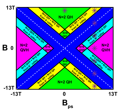
To illustrate above process in detail, we exhibit the phase diagram where a real magnetic field and pseudomagnetic field coexist in Fig. 1. In this diagram, the Fermi level is fixed at . We only focus on those low filling factor phases since is close to the charge neutral point (other higher filling factor phases with more occupied LLs below the Fermi level are denoted by dark blue). To label these QH or QVH phases, the filling factor , i.e. the number of occupied LLs are labeled. In particular, for those valley-imbalanced phases, we use the ‘’ to denote the filling factor of the additional contribution from one valley.
If , as climbs, the energy for each non-zero order LL increases and less LLs are crossed by . Filling factors declines (e.g. the =6 QH phase to the =2 QH phase, see green patches in Fig. 1). Similar situations happen if whereas climbs, except that QH phases are replaced by QVH phases (see magenta patches in Fig. 1). Once and coexist, phases will become complicated. For example, starting from the =2 QH phase ( only exceeds the zeroth LL) with , the energy of the 1st LL from valley will decline and tend to be lower than as increases. After crossing the phase boundary , one more spin-degenerate LL from valley is occupied. We denote this valley-imbalanced phase as ‘=2 QH + =2 QH from valley’. Other phase transition processes are similar, with the phase boundaries or with .
For clarity, the topological phases in Fig. 1 can be further identified by valley Chern numbers . We focus on those within the region and neglect spin-degeneracy. For = QH phases, . For = QVH phases, while . For ‘= QH + = QH from valley’ phase, and . For ‘= QVH + = QH from valley’ phase, and . For ‘= QVH + = QH from valley’ phase, and . The valley Chern numbers for topological phases within the region are just opposite of the above.
These phases in Fig. 1 can be reflected by the spin-degenerate energy bands of a zigzag graphene nanoribbon plotted in Fig. 2. The unit cell length along direction is and the number of lattices is corresponding to a nanoribbon width .
The parameters and follow purple stars in Fig. 1. Figures. 2(a,b,f) belong to the -dominated region and Figs. 2(d,e,h) belong to the -dominated region. Figs. 2(c,g) are two critical points with . To feature these phases, the situations of edge states transport at [denoted by red dotted lines in Fig. 2] are schematically present in insets. It is worth noting that for a zigzag graphene nanoribbon, LL edge states have valley polarizations of valley or valley [59, 60, 61], which are also marked in the insets.
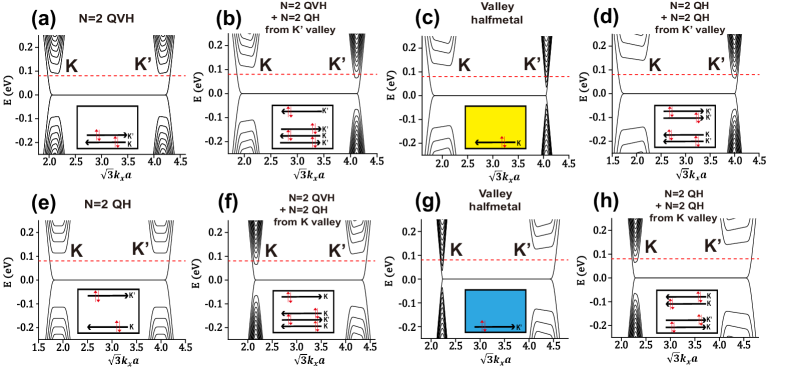
In Figs. 2(a-d), we increase along the positive direction with a fixed . When [Fig. 2(a)], the system is in the =2 QVH phase [magenta patch in Fig. 1] with dispersive pseudomagnetic field-induced LLs [53]. A pair of counterpropagating spin-degenerate edge states at from two valleys locate at only one edge of the graphene nanoribbon [see inset in Fig. 2(a)], unlike two edges in QSH effect [38, 39]. The reasons can be understood on two aspects: (i) Due to the magnetic fields at two valleys are opposite, the edge state of the zeroth LL from the K’ valley should flip its space location, different from the QH edge states which locate at opposite edges in inset in Fig. 2(e). The one-edge valley-polarized channels also correspond to valley Chern number , and no other edge channels appear at the opposite edge. Actually, this special structure of edge states for the zeroth LL is closely related to chiral anomaly [53]. (ii) From the symmetry, these counterpropagating modes at the same edge are implied by time-reversal symmetry [38]. Moreover, inversion symmetry has been broken by strain field in QVH effect, allowing for space asymmetric edge states distributions. Besides, QSH effect and QVH effect also differ in their response to disorders. Different from QSH effect protected by time-reversal symmetry, the QVH effect can exist in the graphene with clean limit or long range disorders, where intervalley scatterings are well suppressed. The short range disorders could couple valleys and destroy the quantized plateaus. The lack of quantization in the presence of the short range disorders may cause some uncertainty on the verification of QVH effect. However, whether the lower edge [see inset in Fig. 2(a)] remains quantized or becomes conductive by short range disorders [38], its longitudinal resistance is always quite different from the other insulating edge where no edge channels exist (the upper edge in the inset in Fig. 2(a)). The latter tends to exhibit an very large resistance but the former exhibit a finite resistance. This asymmetry resistivity of two opposite edges could give some indications on QVH effect. More importantly, QVH effect with valley polarized edge states can be regarded as a quantum inversion of valley Hall effect [62, 63, 64]. Similar to valley Hall effect, when applying the longitudinal voltage, opposite valley polarization or orbital momentum polarization will accumulate at opposite edges in QVH effect through valley polarized edge channels (only one edge accumulates valley polarizations for QVH effect) [65]. This out of plane net magnetization can be detected by Kerr rotation microscopy [66].
When [Fig. 2(b)], the LL energy spacings narrow at valley () but widen at valley (). One more spin-degenerate LL from valley is crossed and additionally contributes two pairs of chiral edge states on the =2 QVH phase. This leads to six edge states appearing at the lower edge while two appearing at the upper edge [see inset in Fig. 2(b)]. The system is thus in the “=2 QVH + =2 QH from valley” phase [cyan patch in Fig. 1]. When [Fig. 2(c)], the gap closes at valley and the energy dispersion astoundingly recovers the Dirac linear dispersion, while the gap and LLs at valley hold. This peculiar phase is a valley halfmetal which was proposed to achieve valley complete polarization transport, since the bulk states all come from one valley [denoted by the yellow color in inset of Fig. 2(c)] [38, 67]. Once [Fig. 2(d)], the total magnetic fields are positive at each valley, the gap opens and LLs at valley form again. Both valleys contribute edge states with the same chirality [see inset in Fig. 2(d)]. Due to one more spin-degenerate LL from valley is crossed (), we name this phase as “=2 QH + =2 QH from valley” [yellow patch in Fig. 1]. When [Fig. 2(e)], the system is in the =2 QH phase [green patch in Fig. 1] and chiral edge states appear at both edges [see inset in Fig. 2(e)] [10]. In Figs. 2(f-h), we fix and increase along the minus direction. The results are similar to Figs. 2(b-d). When , [Fig. 2(f)], one more spin-degenerate LL from valley will be crossed by and contributes two pairs of chiral edge states on the =2 QVH. This is the “=2 QVH + =2 QH from valley” phase, similar to the phase in Fig. 2(b). When [Fig. 2(g)], the gap of valley closes, the energy band recovers the Dirac linear dispersion, and the bulk states all come from valley, which is also a valley halfmetal. Once , the system is in the -dominated region and in QH phases. For example, and in Fig. 2(h), the system is in the “=2 QH + =2 QH from valley” phase. To conclude, from the -dominated region to the -dominated region [e.g. Figs. 2(a-d)], the gap of one valley will close and open. Its edge states will evolve into bulk states and then into edge states again. Therefore, by simply tuning the real magnetic field in the strained graphene, we can control the location of edge states and achieve a valley polarized transport.
At large real magnetic fields, Zeeman splitting may not be neglected. Since the spin along direction is a good quantum number in the presence of the intrinsic SOC, Zeeman effect just simply shifts the spin-up and spin-down bands towards opposite directions of the energy axis by . In view that the free electron factor in graphene is 2 [68], the Zeeman splitting in graphene under is roughly , which is much smaller than LL spacings. So in Fig. 2, the original spin-degenerate bands are slightly split into two spin bands. Correspondingly, the original topological phases shown in Fig. 1 and Fig. 2 will be further divided into spin-polarized QH phases/QVH phases.
IV The QSH effect under a real magnetic field.
In this section, we pay attention to how a real magnetic field affects the QSH phase in graphene. Refs [47, 48, 69] found the QSH phase could be maintained within the SOC energy gap to a large extent of a real magnetic field, even though the time-reversal symmetry is lack. Moreover, due to the contrast between chiral edge states in QH phases and helical edge states in QSH phases, an “unhappy” spin has to reverse its direction of propagation when going from one phase to another [47].
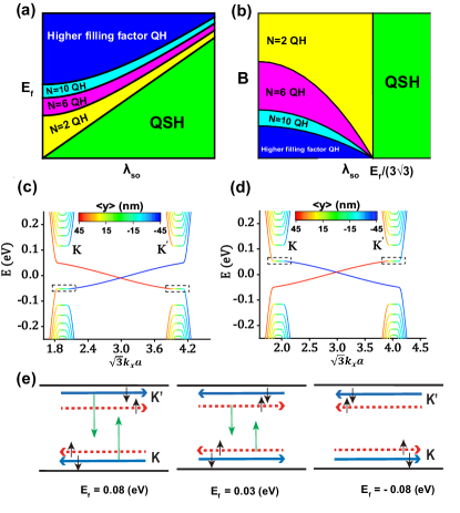
We further illustrate this effect from the perspective of phase diagrams. In Figs. 3(a,b), the phase diagram as a function of the Fermi level and SOC strength with a fixed real magnetic field (a) as well as the phase diagram as a function of the real magnetic field and with a fixed (b) are both shown. According to Table 1 and Ref [47], the phase boundaries should be described by
| (11) |
with . Due to valley and spin degeneracy in graphene [3], the QH phases follow filling factors as climbs with fixed , or as decreases with fixed , . Here only low filling factor QH phases are considered (denoted by yellow, magenta, cyan patches). Other higher filling factor QH phases are denoted by dark blue patches. As long as , the system can keep QSH phase (green patch) [47, 48].
In Figs. 3(c,d), we plot the tight-binding energy bands for the QSH effect under a real magnetic field in a zigzag graphene nanoribbon for the spin-up component and spin-down component . To exhibit the space evolution of the edge states, we compute the expectation values of the position operator for all eigenstates, as shown by the color in Figs. 3(c,d). The edge states for three typical are schematically plotted in Fig. 3(e) (the red dotted arrow line denotes the spin-up channel while the blue solid arrow line denotes the spin-down channel). We emphatically pick out the zeroth LLs for valley and spin-up/down component by black dotted boxes in Figs. 3(c,d). It is clear that the spin degeneracy of the zeroth LL is broken [49, 47]. The energy of the zeroth LL for the spin-up component is and of the zeroth LL for the spin-down component is , which are well consistent with the results in Table. 1. Above the SOC energy gap , this is a typical QH phase with magnetic field-induced LLs [47]. The edge states for two spin components from two valleys have the same chirality [e.g. in Fig. 3(e)]. As goes down, the edge bands from the zeroth LL for the spin-down component will join the zeroth LL flat bands and therewith the edge states will emerge into bulk states [see black dotted boxes in Fig. 3(d)]. Conversely, edge states for the spin-up component stay at one edge since no LL flat bands will be crossed [see Fig. 3(c)]. We use green arrows to show the trend of edge states evolution [see Fig. 3(e), ]. Within the SOC energy gap [e.g. in Fig. 3(e)], the QSH phase keeps [47, 48]. The spin-up and spin-down components contribute two edge states at both edges respectively with the opposite chirality. As continues to descend, edge bands from the zeroth LL for the spin-up component will join the zeroth LL flat bands [see black dotted boxes in Fig. 3(c)] and those edge states tend to emerge into bulk states [indicated by green arrows in Fig. 3(e), ], while edge states for the spin-down component remain still [see Fig. 3(d)]. Below the SOC energy gap [e.g. in Fig. 3(e)], a QH phase is recovered with a reversed chirality since carriers change from the electron type into the hole type. In short, as gradually decreases, the system transitions from the QH phase to the QSH phase and then to the QH phase again. During each transition, we find edge bands for only one spin component (i.e. so-called ‘unhappy’ spin in Ref [47]) cross the zeroth LL flat bands and their edge states leave from one edge into the bulk and further to the other edge, reversing the chirality.
Taking into account Zeeman effect, the spin-up energy band in Fig. 3(a) will be shifted up by and the spin-down energy band in Fig. 3(b) will be shifted down by . The QSH effect region within the zeroth LLs will be slightly narrowed but still persist within the energy range . Since the Zeeman splitting is relatively small, the QSH effect remains in a large extent still. The edge states transition shown in Fig. 3(e) will not change.
V The QSH effect under a pseudomagnetic field.
In last section, from the QSH phase to the QH phase, time-reversal symmetry has been broken and only one spin component changes. For a strain-induced pseudomagnetic field, physical pictures should be different. Especially for edge states from the zeroth LL, they are a pair of spin-degenerate counterpropagating modes from two opposite valleys located at one edge as shown Fig. 2(a), reflecting the space inversion symmetry is broken. In this section, we analyze how a pseudomagnetic field affects the QSH effect.
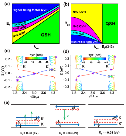
In Figs. 4(a,b), we show the phase diagram as a function of Fermi level and SOC strength with a fixed (a) and the phase diagram as a function of and with a fixed (b). From a perspective of the phase distribution, the situations are basically the same as those under a real magnetic field in Figs. 3(a,b), except that QH phases are replaced by QVH phases.
For the tight-binding energy bands, some details become somehow different. In Figs. 4(c,d), we find the SOC energy gap still keeps like the real magnetic field case. The QSH phase emerges in the SOC energy gap. Outside the SOC energy gap, the space distributions of edge states follow the QVH phase where two time reversal symmetry edge states stay at the same edge [indicated by colors in Figs. 4(c,d)]. For each spin component, the zeroth LLs become no longer energy-degenerate at two valleys [see black dotted boxes in Figs. 4(c,d)]. The energy of the zeroth LL for the spin-up (spin-down) component at valley ( valley) is while at valley ( valley) is , as Table 1 shows. In other words, the zeroth LLs only appear in one branch of decussate energy bands near the charge neutral point [see the color branch in Figs. 4(c,d)] rather than both. For the other branch, the states always stay at one edge since no LL flat bands exist [see the red branch in Figs. 4(c,d)].
These distinctions directly affect the evolution of edge states from the QVH phase to the QSH phase. When Fermi level is above the SOC energy gap, system is in the QVH phase and the counterpropagating edge states from the zeroth LLs stay at lower edge [e.g. in Fig. 4(e)]. As the declines, energy bands for the spin-up component at valley and spin-down component at valley will join the zeroth LL flat bands [see black dotted boxes in Figs. 4(c,d)]. This suggests the time-reversal symmetry and edge states will emerge into bulk states and then go to the upper edge of the nanoribbon [indicated by green arrows in left panel of Fig. 4(e)]. As a result, the QVH phase translates into the QSH phase. Within the SOC energy gap, the helical edge states emerge. The system is in the QSH phase [e.g. in Fig. 4(e)]. As continues to decrease, the edge bands at the upper edge of the nanoribbon start to join the zeroth LL flat bands. These edge states evolve into bulk states again, and then go back to the lower edge. Below the SOC energy gap, a QVH phase recovers and two pairs of time-reversal symmetry edge states from two opposite valleys stay at the lower edge again [the right panel of Fig. 4(e)].
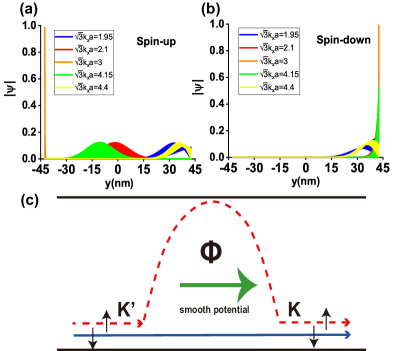
We can exhibit the evolution of the aforementioned edge states through wavefunctions in Figs. 5(a,b). These wavefunctions correspond to points along the rightward energy bands [purple stars in Figs. 4(c,d)]. For the spin-up component [Fig. 5(a)], the wavefunction clearly evolves from the lower edge of the nanoribbon () to the bulk (), then to the upper edge (), next to the bulk () again and finally returns the lower edge (), matching Fig. 4(e) well. While for the spin-down component [Fig. 5(b)], all wavefunctions always stay at the lower edge, due to this band no joining the zeroth LL flat band. In addition, we also notice that the decay length of the QSH edge states is smaller than the LL edge states, because the decay length of the former depends on while the latter depends on [47].
This picture where one spin channel runs from one edge to another edge could be used to conceive a spintronics device to adjust edge states spin direction. In Fig. 5(c), we apply a smooth potential gradient to design a p-n junction. Here only those rightward states are considered since smooth potential makes backscattering nearly unlikely to occur. In the p region and n region, the graphene is in the QVH phase. In the junction, the graphene is in the QSH phase. We also apply a weak real magnetic field on the junction (the coexistence of real magnetic field and pseudomagnetic field will not break our configuration and will be proved in the section VI). Based on previous discussions, one spin channel will surround the junction while the other will keep at one edge. See Fig. 5(c), if we inject a state with the spin polarized in the x direction:
| (12) |
where denotes the eigenstates with the spin-up/down polarized in the direction.
After traversing the junction, the spin-up channel surrounds the junction and accumulates a phase . The spin-down channel keeps at the lower edge and accumulates a phase . Here and are the path for the spin-up and spin-down electrons to transverse the junction. So the outgoing wavefunction should be:
| (13) |
In the last row of Eq. (13), we divide the phase difference of into two parts: is the phase accumulation at the zero real magnetic field while is the flux from the real magnetic field since the two paths and just circle the junction. So we can arbitrarily regulate the relative phase difference between and by adjusting the magnetic flux . In other words, just by varying the magnetic flux, we can continuously rotate the spin polarization direction in the x-y plane of the outgoing state . Our device actually has a similar function as a spin field effect transistor (spin-FET) or Datta-Das transistor which is an electronic analog of the electro-optic modulator [70]. The difference is that we use a QVH-QSH-QVH junction to implement the spin-related Aharonov-Bohm effect [71] to control states spin precession instead of the Rashba SOC.
VI The QSH effect under the coexistence of a real magnetic and a pseudomagnetic field.
In previous sections, we have clarified the relationships between the real magnetic field and the pseudomagnetic field, the real magnetic field and the QSH effect, as well as the pseudomagnetic field and the QSH effect. Now we turn to figure out how these three phases compete and coexist. We still pay attention to phase diagrams, energy bands and edge states. Finally, we design a spintronics multiple-way switch based on the relationship of these three effects.
Referring to Table 1, we naturally generalize the energy of LLs from valley and valley taking into account the SOC :
| (14) |
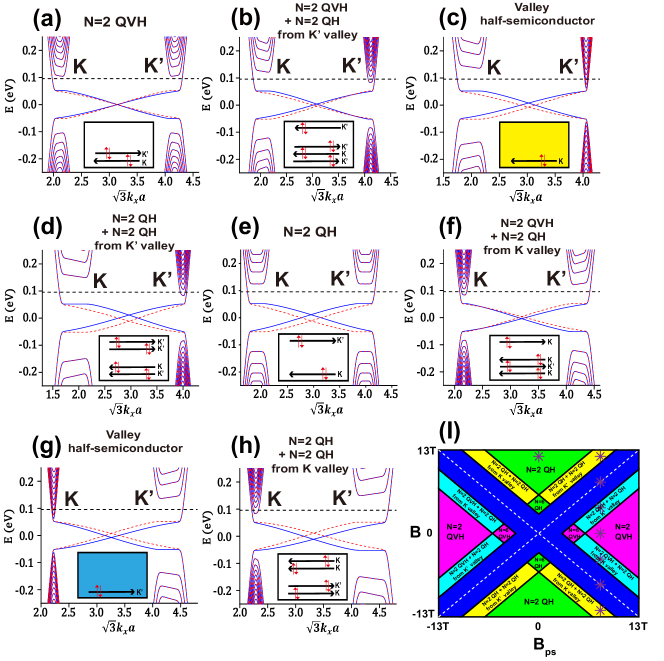
with . The energy of the zeroth LLs for each valley is still with the sign depending on the sign of the total magnetic field. In Figs. 6(a-h), we show the energy bands of a zigzag graphene nanoribbon with , and . We also schematically plot edge states distributions in the insets at Fermi level denoted by black dotted lines in Figs. 6(a-h). Although these results, especially for edge states distributions, are parallel to Fig. 2, some points or discrepancies should be noticed: (1) On the one hand, a SOC energy gap opened by is hardly affected by the real magnetic field and the pseudomagnetic field . The phase of the system depends on where the Fermi level stays. When is within the SOC energy gap, the system is in the QSH phase with a pair of helical edge states, which is independent of and . (2) On the other hand, when is outside the SOC energy gap, the system is in the QH or the QVH phase depending on the real magnetic field or the pseudomagnetic field . As or changes, the system evolves between QH and QVH phases [see Figs. 6(a-h)]. However, from the QH phase to the QVH phase and vice versa, the energy band does not experience a global energy gap close and open. This is quite different from the case of [see Fig. 2]. In other words, and only affect the energy bands outside the SOC energy gap. (3) At the special points , the total magnetic field at one valley disappears. Due to the existence of SOC energy gap, this peculiar energy band should be regarded as a valley half-semiconductor rather than the valley halfmetal [see Figs. 6(c,g) and Figs. 2(c,g)]. In comparison, such a valley half-semiconductor would have stronger application value than a valley halfmetal. Because the valley half-semiconductor has an energy gap, the carrier density can be well controlled. We can adjust the Fermi level to achieve a complete valley-polarized transport ( above the SOC energy gap) and also a spin-related transport ( within the SOC energy gap). (4) The energy bands and edge states above the SOC energy gap can approximately maintain the spin degeneracy, but within the SOC gap the spin degeneracy has been strongly destroyed, since time reversal symmetry and space inversion symmetry are both broken.
The energy bands in Fig. 6 clearly show that when , and coexist, and just compete with each other outside the SOC energy gap. As long as persists, the QSH phase within the SOC energy gap will not be disturbed. Therefore, the phase diagram as a function of and in Fig. 6(i) with Fermi energy fixed at should be identical to Fig. 1.
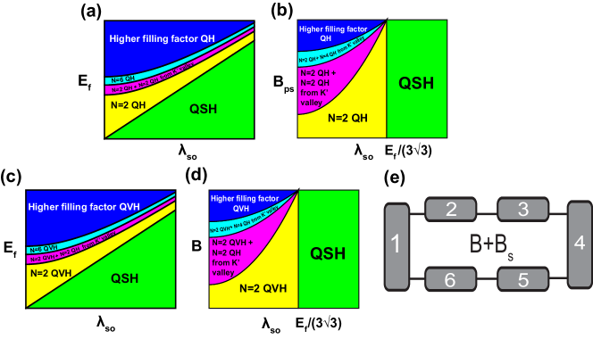
Figures. 7(a-d) show the phase diagrams as a function of and , or () and . Here we still divide the situations into two regions [58]: -dominated [Figs. 7(a,b)] and -dominated [Figs. 7(c,d)]. The phases boundaries are coordinated with Eq. (14). In Figs. 7(a,c), the phase diagram is as a function of and , with a fixed and . separates the QSH phase and the QH phase or the QVH phase . Unlike Fig. 3(a) and Fig. 4(a), an additional valley-imbalanced phase, ‘=2 QH (QVH) + =2 QH from valley’ [see the pink patches in Figs. 7(a,c)], emerges when is between and , since one extra spin-degenerate LL from valley is crossed. Similar situations appear in phase diagrams as a function of () and as well [see Figs. 7(b,d)]. If the is constant and () climbs, according to the Equation (14), more and more LLs from valley will descend and be crossed, echoing valley-imbalanced phases, e.g. the ‘=2 QH (QVH) + =2 (4) QH from valley’ phase denoted by magenta and cyan in Figs. 7(b,d).
Below we also illustrate the edge states distributions of these phases in Figs. 6 and 7. For the QSH phase, a pair of helical edge states with opposite spin channels propagate in opposite directions [16, 17]. The =2 QH, =2 QVH, ‘=2 QH + =2 QH from valley’ and ‘=2 QVH + =2 QH from valley’ phase follow the edge state distributions in Figs. 6(e), (a), (d)/(h), and (b)/(f). For the =6 QH phase, three chiral spin-degenerate edge states appearing at both edges analogy to Fig. 6(e). For the =6 QVH phase, two pairs of counterpropagating spin-degenerate edge states appear at the lower edge while one pair of counterpropagating spin-degenerate edge states appear at the upper edge. For the ‘=2 QH + =4 QH from valley’ phase, three chiral spin-degenerate edge states propagate in opposite directions at opposite edges, analogy to Fig. 6(d). For the ‘=2 QVH + =4 QH from valley’ phase, there are two leftward spin-degenerate edge states at the upper edge, and one leftward spin-degenerate edge states as well as three rightward spin-degenerate edge states at the lower edge.
From the perspective of the transport, we can characterize these aforementioned phases in terms of longitudinal resistance and Hall resistance , by considering a six-terminal device as shown in Fig. 7(e). In the linear response regime, the current flowing from the terminal is calculated by Bttiker formula:[72]
| (15) |
where is the voltage in the terminal and is the transmission coefficients from terminal to terminal . In theoretical calculations, we set that the transmission coefficients are equal to the number of the edge states from terminal to terminal by neglecting disorder-induced backscattering. A voltage is applied on the terminal 1. The terminal 4 is grounded. Other terminals are voltage terminals with zero currents. Along with these conditions, the currents and voltages for each terminal can be obtained by directly solving Equation (15). We note that because space inversion symmetry has been broken by , and are better to define relying on which edge. For the upper edge, . For the lower edge, . The Hall resistances are and .
Based on explicit edge modes distributions in Fig. 6, we can straightly present the calculation results. In the QSH phase, and [16, 17, 69]. For the =2 QH phase in Fig. 6(e), the and . For the =2 QVH phase in Fig. 6(a), [39]. Because edge states of the =2 QVH phase only appear at the lower edge, terminals 2 and 3 are disconnected with the edge states. The voltages and are strongly affected by disorders and hard to be determined, so , and should be uncertain and depend on disorder configurations. For the ‘=2 QH + =2 QH from valley’ phase in Figs. 6(d,h), . for and for . For the ‘=2 QVH + =2 QH from valley’ phase [Fig. 6(b)], , , and . Similarly, for the ‘=2 QVH + =2 QH from valley’ phase [Fig. 6(f)], , , and .
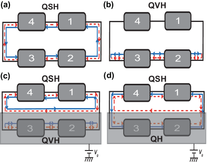
In Ref [47], the QSH phase with a real magnetic field allows for a direct junction between the QSH phase and the QH phase via an additional electrostatic gate. The different chirality for one spin channel will compel it to propagate along the interface. This system thus provides a very efficient spin-polarized charge-current switching mechanism. Compared with the spin flip from the QSH phase to the QH phase, the biggest feature from the QSH phase to the QVH phase is a “side flip” as shown in Fig. 4(e). Enlighten by this, we can use a junction between the QSH phase and the QVH phase to achieve a spintronics multiple-way switch. Considering a four-terminal device, the edge states of the QSH phase () in Fig. 8(a) and the QVH phase () in Fig. 8(b) are shown respectively. A pair of helical edge states with opposite spins propagating in opposite direction appear at both edges in the QSH phase. The counterpropagating spin-degenerate edge states only appear at the lower edge in the QVH phase. We apply a voltage on terminal 1 () and ground all the other terminals . In the QSH phase [Fig. 8(a)], the spin-down current (blue solid arrow lines) will flow from the terminal 1 to the terminal 4 and the spin-up current (red dotted arrow lines) will flow from the terminal 1 to the terminal 2. In the QVH phase [Fig. 8(b)], the upper edge is disconnected and no current flows. Next we combine both effects in Fig. 8(c). If the Fermi level is within the SOC energy gap, the system is still in the QSH phase like Fig. 8(a). When a local top gate is applied on the lower half plane and drives the lower half plane (covered by gray plane) into the QVH phase by adjusting above the SOC energy gap, a direct QSH-QVH junction forms [Fig. 8(c)]. Since the QVH phase only has channels at the lower edge, the spin-up edge flow of the QSH phase cannot flow into the lower half plane and must flow into the terminal 4 through the interface. Hence, by gating the lower half plane into the QSH phase or the QVH phase, we can control the spin-up current from the terminal 1 to flow into the terminal 2 or terminal 4. Furthermore, if a magnetic field is applied on this QSH-QVH junction to magnetize the QVH phase in the lower half plane into the QH phase (the QSH phase will not be interrupted), the spin-up chiral state will emerge along the interface [47] and flow into the terminal 3 and 4 [Fig. 8(d)]. In short, using a local gate and magnetic field on the graphene with SOC and pseudomagnetic field, we can realize a direct junction of QSH-QVH or QSH-QH. This implements a multiple-way spintronics switch to control one spin-polarized current flowing from the terminal 1 into terminals 2,3 and 4.
VII Conclusion.
In summary, we investigate the phase diagrams and edge states transitions when the QH effect, the QSH effect and the QVH effect coexist in graphene. We find the QSH effect can still keep within the SOC energy gap under a relatively large real magnetic field and pseudomagnetic field. Outside the SOC energy gap, the real magnetic field and pseudomagnetic field will compete and affect the LLs at each valley. Moreover, the zeroth LLs of different valleys and spins exhibit different distributions for the real magnetic field and pseudomagnetic field, leading to distinctive edge states transitions from the QSH phase to the QH phase and to the QVH phase. Specially in the case of the pseudomagnetic field, the spatially asymmetric edge state structure can be used to construct a spin FET-like device to tune the spin polarization of edge state transport and realize a multiple-way spintronics switch.
Acknowledgments.
This work was financially supported by NSF-China (Grant No. 11921005), National Key R and D program of China (Grant No. 2017YFA0303301), and the Strategic Priority Research Program of Chinese Academy of Sciences (Grant No. XDB28000000).
Appendix A The effect of strain on the strength of intrinsic SOC
In this appendix, we consider how the strain field modifies the strength for intrinsic SOC and inspect whether it could affect our results in the main text.
In Eq. (2), we directly modify the nearest-neighbor hopping parameters by an exponential relation. For SOC, the situation will be subtle. The intrinsic SOC in graphene originates from the intra-atomic SOC which allows for the transition between the band and band near the Dirac points [73]. Therefore, to include the SOC modifications in the band effective Hamiltonian like Equation (2), the multiple transfer process from to bonds must be considered. From the previous literature, the lowest-order contribution is the next-nearest-neighbor hopping, i.e. passing from to through bonds, and the can be derived as: [23, 24]
| (16) |
where is the energy difference between the and orbitals, is the intra-atomic SOC constant, is the Slater-Koster (SK) parameter formed by and orbitals.
The strain field will change the distance of bonds between lattices and thus correct the . Usually, the variation of SK parameters with the strain can be modeled as an exponential function: [52]
| (17) |
where is the unstrained SK parameter, is a parameter to measure the effect of the strain on the SK parameters and is the distance of the bond formed by and orbitals. We can regard the strain as a small perturbation so the Equation (16) is still valid. Putting Equation (17) into Equation (16), we can derive a relation:
| (18) |
Here is the SOC strength depending on the next-nearest-neighbor lattice indices and . denotes the middle lattice site when passing from to . is the unstrained SOC strength. Equation (18) is very similar to the Equation (2) except that the minus sign in the exponential changes into the plus sign. takes the role of in Equation (2) with a value around 2 [74].
Now we investigate if is modified as in Equation (18), what the SOC term (the second term in Equation (1)) could bring about. For each lattice point, we denote its six next-nearest-neighbor SOC strength as . Using the Fourier transformation, can be transformed into the Brillouin zone under the basis :
| (19) |
Here denotes the next-nearest-neighbor bond and is the bond vector of the next-nearest-neighbor bond [75]. Using the linear expansion and the relation , we can expand near the Dirac point :
| (20) |
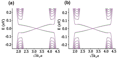
In the last equality of Equation (20), we ignore the contribution from which is a small amount around the Dirac point. The first term of the last equality is the zeroth contribution of the SOC which is just a mass term as Equation (9) indicates. The second term is the first correction of SOC and should be tiny since is generally smaller than . The third term should be also neglected as it is small too and irrelevant to SOC strength modulation. Therefore, the modification from strain on the SOC strength should not affect our results, in view that the main contributions come from the SOC zeroth contribution. This is different from the case for the nearest-neighbor hopping modulations where the zeroth contributions disappear at the Dirac points. As for and valley, situations are alike. Furthermore, in Figs. 9(a,b), we plot the energy bands with SOC corrections (magenta dotted lines) and without SOC corrections (olive green solid lines). It is clear that results are almost identical.
Appendix B The effect of Rashba SOC
In this appendix, we theoretically study how the topological phases are affected by Rashba SOC. If the mirror symmetry is broken by a perpendicular electric field or by the interaction with a substrate, a Rashba SOC will arise in the Kane-Mele model with a term [18, 19]:
| (21) |
where is the strength of Rashba SOC. Without the real magnetic and pseudomagnetic field, the Rashba SOC has two effects on Kane-Mele model in Eq. (9): (i) breaking the spin conservation along direction, (ii) destroying the intrinsic SOC gap 2. For , the energy gap 2 () remains finite and QSH effect keeps. For , the energy gap closes and reopens with QSH phase disappearing [18, 19].
When in the presence of both the Rashba SOC and the (pseudo)magnetic field (), the low-energy Hamiltonian for valley is:
| (22) |
where or . Under a real magnetic field, the Hamiltonian for is related to by a time-reversal transformation: . While under a pseudomagnetic field, the Hamiltonian for is related to by a time-reversal transformation: . Taking as an example and solving the equation in Eq. (22), the LL energy is (): [49]
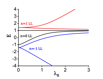
| (23) |
It can be verified this energy relation is both valid for and no matter under a real magnetic or a pseudomagnetic field. It indicates the energy of LLs at and valleys is similar, and their wavefunctions are related by time-reversal transformation. We can just pay attention on valley. The general solution of Eq. (23) is a little more complex than results in Table. 1 and can be consulted in details in Ref. [49]. In Fig. 10, we focus on the energy variation of three lowest LLs ( LL and LLs) versus . For convenience, we take . When , the LLs are spin-degenerate at , while the zeroth LLs are spin degeneracy broken at , which is consistent with the LLs distributions in Table. I, Fig. 3 and Fig. 4. As the climbs, the spin along direction is no longer a good quantum number and the spin-degenerate LLs are split into two spin bands respectively (see Fig. 10). Differently, the LL with higher energy stays at always, while the LL with lower energy starts to approach from (no energy crossing). The former is attributed to is always one solution of Eq. (23) for . Thus, the original SOC gap at and valley within the zeroth LLs (denoted by black boxes in Fig. 3 and Fig. 4) is shrunk by the Rashba SOC and QSH phase will be totally cannibalized once is very large. Outside the SOC gap, since spin-degenerate LLs are lifted, the QH phases/QVH phases may evolve into spin-polarized QH phases/QVH phases.
References
- Geim [2009] A. K. Geim, Graphene: Status and Prospects, Science 324, 1530 (2009).
- Geim and Novoselov [2007] A. K. Geim and K. S. Novoselov, The rise of graphene, Nat. Mater. 6, 183 (2007).
- Castro Neto et al. [2009] A. H. Castro Neto, F. Guinea, N. M. R. Peres, K. S. Novoselov, and A. K. Geim, The electronic properties of graphene, Rev. Mod. Phys. 81, 109 (2009).
- Novoselov et al. [2005] K. S. Novoselov, A. K. Geim, S. V. Morozov, D. Jiang, M. I. Katsnelson, I. V. Grigorieva, S. V. Dubonos, and A. A. Firsov, Two-dimensional gas of massless Dirac fermions in graphene, Nature (London) 438, 197 (2005).
- Mikitik and Sharlai [1999] G. P. Mikitik and Y. V. Sharlai, Manifestation of Berry’s Phase in Metal Physics, Phys. Rev. Lett. 82, 2147 (1999).
- Hou et al. [2019] Z. Hou, Y.-F. Zhou, X. C. Xie, and Q.-F. Sun, Berry phase induced valley level crossing in bilayer graphene quantum dots, Phys. Rev. B 99, 125422 (2019).
- Ren et al. [2022] Y.-N. Ren, Q. Cheng, Q.-F. Sun, and L. He, Realizing Valley-Polarized Energy Spectra in Bilayer Graphene Quantum Dots via Continuously Tunable Berry Phases, Phys. Rev. Lett. 128, 206805 (2022).
- Zhang et al. [2005] Y. Zhang, Y.-W. Tan, H. L. Stormer, and P. Kim, Experimental observation of the quantum Hall effect and Berry’s phase in graphene, Nature (London) 438, 201 (2005).
- Goerbig [2011] M. O. Goerbig, Electronic properties of graphene in a strong magnetic field, Rev. Mod. Phys. 83, 1193 (2011).
- Castro Neto et al. [2006] A. H. Castro Neto, F. Guinea, and N. M. R. Peres, Edge and surface states in the quantum Hall effect in graphene, Phys. Rev. B 73, 205408 (2006).
- Peres et al. [2006] N. M. R. Peres, F. Guinea, and A. H. Castro Neto, Electronic properties of disordered two-dimensional carbon, Phys. Rev. B 73, 125411 (2006).
- Novoselov et al. [2007] K. S. Novoselov, Z. Jiang, Y. Zhang, S. V. Morozov, H. L. Stormer, U. Zeitler, J. C. Maan, G. S. Boebinger, P. Kim, and A. K. Geim, Room-Temperature Quantum Hall Effect in Graphene, Science 315, 1379 (2007).
- Brey and Fertig [2006] L. Brey and H. A. Fertig, Edge states and the quantized Hall effect in graphene, Phys. Rev. B 73, 195408 (2006).
- Long et al. [2008] W. Long, Q.-f. Sun, and J. Wang, Disorder-Induced Enhancement of Transport through Graphene Junctions, Phys. Rev. Lett. 101, 166806 (2008).
- Chen et al. [2010] J.-c. Chen, T. C. A. Yeung, and Q.-f. Sun, Effect of disorder on longitudinal resistance of a graphene junction in the quantum Hall regime, Phys. Rev. B 81, 245417 (2010).
- Hasan and Kane [2010] M. Z. Hasan and C. L. Kane, Colloquium: Topological insulators, Rev. Mod. Phys. 82, 3045 (2010).
- Qi and Zhang [2011] X.-L. Qi and S.-C. Zhang, Topological insulators and superconductors, Rev. Mod. Phys. 83, 1057 (2011).
- Kane and Mele [2005a] C. L. Kane and E. J. Mele, Quantum Spin Hall Effect in Graphene, Phys. Rev. Lett. 95, 226801 (2005a).
- Kane and Mele [2005b] C. L. Kane and E. J. Mele, topological Order and the Quantum Spin Hall Effect, Phys. Rev. Lett. 95, 146802 (2005b).
- Haldane [1988] F. D. M. Haldane, Model for a Quantum Hall Effect without Landau Levels: Condensed-Matter Realization of the ”Parity Anomaly”, Phys. Rev. Lett. 61, 2015 (1988).
- Lü and Xie [2019] X.-L. Lü and H. Xie, Spin Filters and Switchers in Topological-Insulator Junctions, Phys. Rev. Applied 12, 064040 (2019).
- Jiang et al. [2009] H. Jiang, S. Cheng, Q.-f. Sun, and X. C. Xie, Topological Insulator: A New Quantized Spin Hall Resistance Robust to Dephasing, Phys. Rev. Lett. 103, 036803 (2009).
- Min et al. [2006] H. Min, J. E. Hill, N. A. Sinitsyn, B. R. Sahu, L. Kleinman, and A. H. MacDonald, Intrinsic and Rashba spin-orbit interactions in graphene sheets, Phys. Rev. B 74, 165310 (2006).
- Yao et al. [2007] Y. Yao, F. Ye, X.-L. Qi, S.-C. Zhang, and Z. Fang, Spin-orbit gap of graphene: First-principles calculations, Phys. Rev. B 75, 041401(R) (2007).
- Weeks et al. [2011] C. Weeks, J. Hu, J. Alicea, M. Franz, and R. Wu, Engineering a Robust Quantum Spin Hall State in Graphene via Adatom Deposition, Phys. Rev. X 1, 021001 (2011).
- Jiang et al. [2012] H. Jiang, Z. Qiao, H. Liu, J. Shi, and Q. Niu, Stabilizing Topological Phases in Graphene via Random Adsorption, Phys. Rev. Lett. 109, 116803 (2012).
- Balakrishnan et al. [2013] J. Balakrishnan, G. Kok Wai Koon, M. Jaiswal, A. H. Castro Neto, and B. Özyilmaz, Colossal enhancement of spin-orbit coupling in weakly hydrogenated graphene, Nat. Phys. 9, 284 (2013).
- Avsar et al. [2014] A. Avsar, J. Y. Tan, T. Taychatanapat, J. Balakrishnan, G. K. W. Koon, Y. Yeo, J. Lahiri, A. Carvalho, A. S. Rodin, E. C. T. O’Farrell, G. Eda, A. H. Castro Neto, and B. Özyilmaz, Spin-orbit proximity effect in graphene, Nat. Commun. 5, 4875 (2014).
- Wang et al. [2015] Z. Wang, D.-K. Ki, H. Chen, H. Berger, A. H. MacDonald, and A. F. Morpurgo, Strong interface-induced spin-orbit interaction in graphene on WS2, Nat. Commun. 6, 8339 (2015).
- Avsar et al. [2020] A. Avsar, H. Ochoa, F. Guinea, B. Özyilmaz, B. J. van Wees, and I. J. Vera-Marun, Colloquium: Spintronics in graphene and other two-dimensional materials, Rev. Mod. Phys. 92, 021003 (2020).
- Lee et al. [2008] C. Lee, X. Wei, J. W. Kysar, and J. Hone, Measurement of the Elastic Properties and Intrinsic Strength of Monolayer Graphene, Science 321, 385 (2008).
- Pereira and Castro Neto [2009] V. M. Pereira and A. H. Castro Neto, Strain Engineering of Graphene’s Electronic Structure, Phys. Rev. Lett. 103, 046801 (2009).
- Amorim et al. [2016] B. Amorim, A. Cortijo, F. de Juan, A. G. Grushin, F. Guinea, A. Gutiérrez-Rubio, H. Ochoa, V. Parente, R. Roldán, P. San-Jose, J. Schiefele, M. Sturla, and M. A. H. Vozmediano, Novel effects of strains in graphene and other two dimensional materials, Phys. Rep. 617, 1 (2016).
- Peres [2010] N. M. R. Peres, Colloquium: The transport properties of graphene: An introduction, Rev. Mod. Phys. 82, 2673 (2010).
- Guinea et al. [2008] F. Guinea, B. Horovitz, and P. Le Doussal, Gauge field induced by ripples in graphene, Phys. Rev. B 77, 205421 (2008).
- Masir et al. [2013] M. R. Masir, D. Moldovan, and F. Peeters, Pseudo magnetic field in strained graphene: Revisited, Solid State Commun 175-176, 76 (2013).
- Guinea et al. [2010] F. Guinea, M. I. Katsnelson, and A. K. Geim, Energy gaps and a zero-field quantum Hall effect in graphene by strain engineering, Nat. Phys. 6, 30 (2010).
- Low and Guinea [2010] T. Low and F. Guinea, Strain-Induced Pseudomagnetic Field for Novel Graphene Electronics, Nano Lett 10, 3551 (2010).
- Wu et al. [2021] B.-L. Wu, Q. Wei, Z.-Q. Zhang, and H. Jiang, Transport property of inhomogeneous strained graphene, Chin. Phys. B 30, 030504 (2021).
- Levy et al. [2010] N. Levy, S. A. Burke, K. L. Meaker, M. Panlasigui, A. Zettl, F. Guinea, A. H. C. Neto, and M. F. Crommie, Strain-Induced Pseudo-Magnetic Fields Greater Than 300 Tesla in Graphene Nanobubbles, Science 329, 544 (2010).
- Jiang et al. [2017] Y. Jiang, J. Mao, J. Duan, X. Lai, K. Watanabe, T. Taniguchi, and E. Y. Andrei, Visualizing Strain-Induced Pseudomagnetic Fields in Graphene through an hBN Magnifying Glass, Nano Lett 17, 2839 (2017).
- Mao et al. [2020] J. Mao, S. P. Milovanović, M. Andelković, X. Lai, Y. Cao, K. Watanabe, T. Taniguchi, L. Covaci, F. M. Peeters, A. K. Geim, Y. Jiang, and E. Y. Andrei, Evidence of flat bands and correlated states in buckled graphene superlattices, Nature (London) 584, 215 (2020).
- Meng et al. [2013] L. Meng, W.-Y. He, H. Zheng, M. Liu, H. Yan, W. Yan, Z.-D. Chu, K. Bai, R.-F. Dou, Y. Zhang, Z. Liu, J.-C. Nie, and L. He, Strain-induced one-dimensional Landau level quantization in corrugated graphene, Phys. Rev. B 87, 205405 (2013).
- Georgi et al. [2017] A. Georgi, P. Nemes-Incze, R. Carrillo-Bastos, D. Faria, S. Viola Kusminskiy, D. Zhai, M. Schneider, D. Subramaniam, T. Mashoff, N. M. Freitag, M. Liebmann, M. Pratzer, L. Wirtz, C. R. Woods, R. V. Gorbachev, Y. Cao, K. S. Novoselov, N. Sandler, and M. Morgenstern, Tuning the Pseudospin Polarization of Graphene by a Pseudomagnetic Field, Nano Lett 17, 2240 (2017).
- Jia et al. [2019] P. Jia, W. Chen, J. Qiao, M. Zhang, X. Zheng, Z. Xue, R. Liang, C. Tian, L. He, Z. Di, and X. Wang, Programmable graphene nanobubbles with three-fold symmetric pseudo-magnetic fields, Nat. Commun. 10, 3127 (2019).
- Zhu et al. [2015] S. Zhu, J. A. Stroscio, and T. Li, Programmable Extreme Pseudomagnetic Fields in Graphene by a Uniaxial Stretch, Phys. Rev. Lett. 115, 245501 (2015).
- Shevtsov et al. [2012] O. Shevtsov, P. Carmier, C. Petitjean, C. Groth, D. Carpentier, and X. Waintal, Graphene-Based Heterojunction between Two Topological Insulators, Phys. Rev. X 2, 031004 (2012).
- Beugeling et al. [2012] W. Beugeling, N. Goldman, and C. M. Smith, Topological phases in a two-dimensional lattice: Magnetic field versus spin-orbit coupling, Phys. Rev. B 86, 075118 (2012).
- De Martino et al. [2011] A. De Martino, A. Hütten, and R. Egger, Landau levels, edge states, and strained magnetic waveguides in graphene monolayers with enhanced spin-orbit interaction, Phys. Rev. B 84, 155420 (2011).
- He and He [2013] W.-Y. He and L. He, Coupled spin and pseudomagnetic field in graphene nanoribbons, Phys. Rev. B 88, 085411 (2013).
- Lee et al. [2017] S.-P. Lee, D. Nandi, F. Marsiglio, and J. Maciejko, Fractional josephson effect in nonuniformly strained graphene, Phys. Rev. B 95, 174517 (2017).
- Pereira et al. [2009] V. M. Pereira, A. H. Castro Neto, and N. M. R. Peres, Tight-binding approach to uniaxial strain in graphene, Phys. Rev. B 80, 045401 (2009).
- Lantagne-Hurtubise et al. [2020] É. Lantagne-Hurtubise, X.-X. Zhang, and M. Franz, Dispersive Landau levels and valley currents in strained graphene nanoribbons, Phys. Rev. B 101, 085423 (2020).
- Settnes et al. [2016] M. Settnes, S. R. Power, and A.-P. Jauho, Pseudomagnetic fields and triaxial strain in graphene, Phys. Rev. B 93, 035456 (2016).
- Li et al. [2015] S.-Y. Li, K.-K. Bai, L.-J. Yin, J.-B. Qiao, W.-X. Wang, and L. He, Observation of unconventional splitting of landau levels in strained graphene, Phys. Rev. B 92, 245302 (2015).
- Li et al. [2020] S.-Y. Li, Y. Su, Y.-N. Ren, and L. He, Valley Polarization and Inversion in Strained Graphene via Pseudo-Landau Levels, Valley Splitting of Real Landau Levels, and Confined States, Phys. Rev. Lett. 124, 106802 (2020).
- Roy [2011] B. Roy, Odd integer quantum Hall effect in graphene, Phys. Rev. B 84, 035458 (2011).
- Roy et al. [2013] B. Roy, Z.-X. Hu, and K. Yang, Theory of unconventional quantum Hall effect in strained graphene, Phys. Rev. B 87, 121408(R) (2013).
- Tworzydło et al. [2007] J. Tworzydło, I. Snyman, A. R. Akhmerov, and C. W. J. Beenakker, Valley-isospin dependence of the quantum Hall effect in a graphene junction, Phys. Rev. B 76, 035411 (2007).
- Beenakker [2008] C. W. J. Beenakker, Colloquium: Andreev reflection and Klein tunneling in graphene, Rev. Mod. Phys. 80, 1337 (2008).
- Trifunovic and Brouwer [2019] L. Trifunovic and P. W. Brouwer, Valley isospin of interface states in a graphene junction in the quantum Hall regime, Phys. Rev. B 99, 205431 (2019).
- Mak et al. [2014] K. F. Mak, K. L. McGill, J. Park, and P. L. McEuen, The valley Hall effect in MoS2 transistors, Science 344, 1489 (2014).
- Sui et al. [2015] M. Sui, G. Chen, L. Ma, W.-Y. Shan, D. Tian, K. Watanabe, T. Taniguchi, X. Jin, W. Yao, D. Xiao, and Y. Zhang, Gate-tunable topological valley transport in bilayer graphene, Nature Phys 11, 1027 (2015).
- Lensky et al. [2015] Y. D. Lensky, J. C. W. Song, P. Samutpraphoot, and L. S. Levitov, Topological Valley Currents in Gapped Dirac Materials, Phys. Rev. Lett. 114, 256601 (2015).
- Bhowal and Vignale [2021] S. Bhowal and G. Vignale, Orbital Hall effect as an alternative to valley Hall effect in gapped graphene, Phys. Rev. B 103, 195309 (2021).
- Lee et al. [2016] J. Lee, K. F. Mak, and J. Shan, Electrical control of the valley Hall effect in bilayer MoS2 transistors, Nature Nanotech 11, 421 (2016).
- Settnes et al. [2017] M. Settnes, J. H. Garcia, and S. Roche, Valley-polarized quantum transport generated by gauge fields in graphene, 2D Materials 4, 031006 (2017).
- Volkov et al. [2012] A. V. Volkov, A. A. Shylau, and I. V. Zozoulenko, Interaction-induced enhancement of factor in graphene, Phys. Rev. B 86, 155440 (2012).
- Chen et al. [2012] J.-c. Chen, J. Wang, and Q.-f. Sun, Effect of magnetic field on electron transport in HgTe/CdTe quantum wells: Numerical analysis, Phys. Rev. B 85, 125401 (2012).
- Datta and Das [1990] S. Datta and B. Das, Electronic analog of the electro-optic modulator, Appl. Phys. Lett 56, 665 (1990).
- Aharonov and Bohm [1959] Y. Aharonov and D. Bohm, Significance of Electromagnetic Potentials in the Quantum Theory, Phys. Rev. 115, 485 (1959).
- Büttiker [1986] M. Büttiker, Four-Terminal Phase-Coherent Conductance, Phys. Rev. Lett. 57, 1761 (1986).
- Huertas-Hernando et al. [2006] D. Huertas-Hernando, F. Guinea, and A. Brataas, Spin-orbit coupling in curved graphene, fullerenes, nanotubes, and nanotube caps, Phys. Rev. B 74, 155426 (2006).
- Rezaei and Phirouznia [2018] H. Rezaei and A. Phirouznia, Modified spin-orbit couplings in uniaxially strained graphene, Eur. Phys. J. B 91, 295 (2018).
- Lu et al. [2021] W.-T. Lu, Q.-F. Sun, Y.-F. Li, and H.-Y. Tian, Spin-valley polarized edge states and quantum anomalous Hall states controlled by side potential in two-dimensional honeycomb lattices, Phys. Rev. B 104, 195419 (2021).