Overdamped Phase Diffusion in hBN Encapsulated Graphene Josephson Junctions
Abstract
We investigate the zero-bias behavior of Josephson junctions made of encapsulated graphene boron nitride heterostructures in the long ballistic junction regime. For temperatures down to K, the junctions appear non-hysteretic with respect to the switching and retrapping currents and . A small non-zero resistance is observed even around zero bias current, and scales with temperature as dictated by the phase diffusion mechanism. By varying the graphene carrier concentration we are able to confirm that the observed phase diffusion mechanism follows the trend for an overdamped Josephson junction. This is in contrast with the majority of graphene-based junctions which are underdamped and shorted by the environment at high frequencies.
Graphene-based superconductor-normal metal-superconductor (SNS) Josephson junctions have been a popular medium of choice for studying the fundamentals(Heersche et al., 2007; Miao et al., 2007; Du et al., 2008; Ojeda-Aristizabal et al., 2009; Borzenets et al., 2011; Ke et al., 2016; Lee et al., 2011; Coskun et al., 2012; Borzenets et al., 2016a; Shalom et al., 2015; Larson et al., 2020) as well as applications(Borzenets et al., 2016b, 2013; Amet et al., 2016; Wei et al., 2019; Lee et al., 2017; Park et al., 2017) of superconducting devices for more than a decade. However, the full spectrum and consequences of the interactions between the graphene Josephson junction and the environment have not been fully mapped. For example, the observed critical current of graphene Josephson junctions is consistently suppressed compared to theoretical predictions; leading to postulations that the junctions are severely underdamped(Tinkham, 2004; Borzenets et al., 2011; Ke et al., 2016; Borzenets et al., 2016a; Shalom et al., 2015), despite the relatively low hysteresis between the switching and the retrapping currents. The effect of a junction’s environment on its dynamics can be directly investigated by looking at the statistical distribution of the switching current (Borzenets et al., 2016a; Coskun et al., 2012; Lee et al., 2011; Fulton and Dunkleberger, 1974; Clarke et al., 1988), or via the measurement of zero-bias resistance arising from the phase diffusion mechanism(Tinkham, 2004; Borzenets et al., 2011; Ingold et al., 1994; Martinis and Kautz, 1989; Kautz and Martinis, 1990; Ivanchenko and Zil’berman, 1968, 1969). Indeed, often attributed to the large capacitance generated by the bonding pads and leads, previous works have shown that the vast majority of graphene-based JJs are underdamped(Borzenets et al., 2011; Ke et al., 2016; Shalom et al., 2015; Borzenets et al., 2016a).
In this work we report on Josephson junctions made from hexagonal boron-nitride (hBN) encapsulated graphene with Molybdenum-Rhenium (MoRe) alloy superconducting contacts (Wang et al., 2013; Wei et al., 2019; Amet et al., 2016). These devices are governed by ballistic electron transport and have been found to be in the intermediate to long-junction regime(Borzenets et al., 2016a) (see supplementary). Here, the MoRe contacts terminate shortly after the active region and are connected to the bonding pads via thin Gold leads. Moreover, the MoRe-Au interface seems to exhibit a significant contact resistance. The junctions were measured at temperatures between and K, where a clear phase diffusion governed, zero-bias resistance can be observed(Tinkham, 2004; Borzenets et al., 2011; Ingold et al., 1994; Martinis and Kautz, 1989; Kautz and Martinis, 1990; Ivanchenko and Zil’berman, 1968, 1969). However, for these devices, when changing the carrier concentration via the back gate, the zero-bias resistance follows the trend expected for overdamped junctions(Borzenets et al., 2011; Ivanchenko and Zil’berman, 1969; Ambegaokar and Halperin, 1969). Thus, we conclude that we have demonstrated ballistic graphene Josephson junction in the overdamped regime.
Graphene is made using the exfoliation method(Novoselov et al., 2005) and is encapsulated in hexagonal boron-nitride (hBN) using the “pick-up” method (Wang et al., 2013). Using CHF3/O2 plasma, the hBN-Grahpene-hBN stack is etched thorough in order to make quasi-one dimensional electrical contacts with superconducting electrodes(Amet et al., 2016). Molybdenum-Rhenium(MoRe) alloy electrodes are deposited onto the device using DC sputtering with the approximate thickness of nm. The bonding pads and thin metal leads making contact to MoRe are made of Cr/Au (nm/nm). Here, we present data on the device of length (the distance between MoRe contacts), and the width (see supplementary).
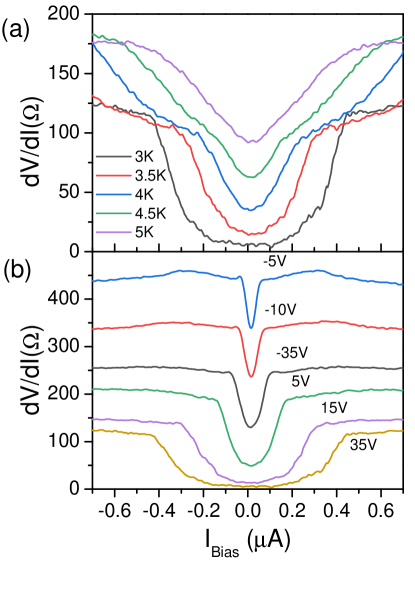
The device is measured in a home-made cryocooler with a base temperature of 2.5K, which is isolated via both a heat shield and RC filters placed at the low temperature stage. Josephson junction resistance is measured using the lockin method with a four-probe geometry. The junction is biased by a variable DC current with a small AC excitation of nA. The voltage across the junction is amplified using a custom differential pre-amp prior to being fed into the lockin. The gate voltage applied to the back of the 300nm SiO2 oxide layer is used to control the carrier density of graphene. Figure 1 presents the differential resistance as a function of applied DC bias current . All the curves show two transition points, as the bias current is swept from a large negative value to a large positive value. The absolute value of the current on the negative side below which the junction becomes superconducting is the retrapping current , i.e. . On the positive side, the junction transitions from the superconducting to the normal state at the switching current (Tinkham, 2004). Figure 1(a) shows resistance versus for different temperatures with the backgate voltage set to 35V. Figure 1(b) shows the resistance versus bias current for different gate voltages taken at 3K. In both cases, the switching and retrapping currents and follow the expected trends: falling exponentially with increasing temperature, and increasing with gate voltage away from the Dirac point with the hole conduction regime exhibiting a suppressed critical current due to the effects of contact doping(Borzenets et al., 2011; Ke et al., 2016; Borzenets et al., 2016a). Moreover, the trend of with respect to temperature follows that expected for ballistic Josephson junctions in the long junction regime (See Supplementary)(Borzenets et al., 2016a).
The vast majority of previously reported graphene Josephson junctions, exhibit hysteresis between the switching and retrapping currents, with even for temperatures above 3K. While certain works attribute this hysteresis to self-heating of the junction(Borzenets et al., 2013; Courtois et al., 2008), it has also been shown that most of the graphene Josephson junctions exhibit underdamped behavior(Borzenets et al., 2011; Ke et al., 2016; Shalom et al., 2015; Borzenets et al., 2016a). (Graphene-based Josephson junctions a typically overdamped due to the large capacitance caused by the presence of the backgate.) Here, however, for all tested gates and temperatures, we do not observe a difference between and . This leads to an initial indication that the device may be overdamped.
We now further investigate the junction dynamics via the characterization of device behavior in the phase diffusion regime. Phase diffusion manifests itself as an observable non-zero resistance below the critical current (even at ), arising from phase slips that are caused by thermal noise. The rate of these phase slips down the prototypical titled washboard potential, and therefore, the measured zero-bias resistance is governed by the junction dynamics which dictate the energy dissipation rate(Tinkham, 2004). Indeed, we are able to observe a measurable resistance in our devices, even at zero bias, and down to 3K in temperature. We define the measured zero-bias differential resistance as R0. In order to confirm that arises from the phase diffusion mechanism, we study the evolution of this resistance with respect to temperature. Regardless of the junction damping dynamics the trend behavior of with respect to temperature should have the following dependence: (Tinkham, 2004; Borzenets et al., 2011; Ingold et al., 1994; Martinis and Kautz, 1989; Kautz and Martinis, 1990; Ivanchenko and Zil’berman, 1968, 1969; Ambegaokar and Halperin, 1969):
| (1) |
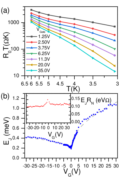
Here, is the Josephson energy. (The above exponential dependence holds when (Tinkham, 2004).) Reworking equation (1), we can arrive at the proportionality relationship: . In Figure 2a we plot the value versus inverse temperature on a semi-log scale. Indeed, we find that the relationship is nearly linear, consistent with theory. From here, knowing the temperature, we can extract from the slope of the curves. The fitted Josephson energy versus gate voltage is plotted in Figure 2b. For single layer graphene Josephson junctions governed by ballistic transport it is expected that value is constant with respect to (Borzenets et al., 2016a); and we find not only that indeed this is the case (see Figure 2 inset), but that this value matched well with the expected energy scale extracted from the trend of vs (see supplementary). Here is the normal resistance, i.e. the resistance of the junction when it is in normal state.
Having found the Josephson energy, we can determine the last parameter governing . This final parameter is different depending on the damping dynamics of the junction. Previous theoretical works have defined three different regimes: For overdamped junctions, the governing parameter is , the normal resistance(Ivanchenko and Zil’berman, 1969; Ambegaokar and Halperin, 1969). For underdamped junctions, depends on the plasma frequency (Kautz and Martinis, 1990). (Here is the capacitance of the junction.) Finally, if the junction is underdamped at low frequencies, but becomes overdamped at the plasma frequency (due to being shorted by the environment), we have (Ingold et al., 1994). Here is the real part of the high frequency impedance caused by the junction’s environment (Ingold et al., 1994). We find that analyzing our devices as if they were underdamped, or damped by the environment does not produce a good match between measured data and theoretical expectation. (See supplementary).
Now, we confirm that our devices are indeed in the overdamped regime by comparing the measured normal resistance with that back calculated from the the zero-bias resistance . Following the full expression in Ref. (Ambegaokar and Halperin, 1969) we have:
| (2) |
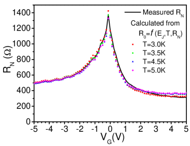
Here, I0 is the modified Bessel function, and . ( is the voltage measured accross the junction.) For approaching zero, the equation simplifies to . Figure 3 shows the measured normal resistance versus gate voltage plotted together with the resistance calculated from Equation 2 for different temperatures. It can be seen that we have a good match between the measured and the theoretical result, in particular for high values of .
The damping of the junction is typically determined by the quality factor , with . ( being the capacitance of the junction.) A results in an overdamped junction(Likharev, 1991). However, the difficulty in calculating an accurate quality factor is two fold: One, the measured critical current has been consistently less than the value predicted by theory, leading to the question of whether the true critical current is being measured. Two, it is unclear which areas of the device play an active role in the junction capacitance . (Previous works have suggested that the capacitance all the way up to the capacitive coupling between the device bonding pads plays a significant role. Thus the junction capacitance is always several orders of magnitude larger compared to that expected from the dimensions of the SNS region itself.) Assuming that the junction capacitance includes the contribution of the bonding pads that couple to each other via the backgate below the thick layer, we arrive at . Taking and , we calculate a quality factor : the underdamped regime. Hence, we are led to conclude that the tested junction has been sufficiently isolated from the capacitive contribution of the bonding pads. Indeed, we estimate that the interface between MoRe superconducting contacts and the gold leads suffers from a contact resistance in the order of tens of , which is sufficient to reduce the quality factor below Vion et al. (1996); Borzenets et al. (2013).
In conclusion, we have investigated the phase diffusion regime in hBN encapsulated graphene Josephson junction governed by ballistic electron transport. The observed trend of the measured zero-bias resistance with respect to carrier concentration conforms well to theory describing phase diffusion in an overdamped junction regime. This is the first conclusive confirmation of overdamped behavior in graphene-based Josephson junction. We attribute this behavior to effective isolation of the Josephson junction from the capacitive contribution of the bonding pads. The isolation arises from a resistive connection with the device layout.
Acknowledgements.
J.T., A.Sh., and I.V.B. acknowledge CityU New Research Initiatives/Infrastructure Support from Central (APRC): 9610395, and the Hong Kong Research Grants Council Projects: (ECS) 2301818, (GRF) 11303619. Lithographic fabrication and characterization of the samples performed by E.G.A., and A.S. were supported by the Division of Materials Sciences and Engineering, Office of Basic Energy Sciences, U.S. Department of Energy, under Award DE-SC0002765.References
- Heersche et al. (2007) H. B. Heersche, P. Jarillo-Herrero, J. B. Oostinga, L. M. K. Vandersypen, and A. F. Morpurgo, Nature 446, 56 (2007).
- Miao et al. (2007) F. Miao, S. Wijeratne, Y. Zhang, U. C. Coskun, W. Bao, and C. N. Lau, Science 317, 1530 (2007).
- Du et al. (2008) X. Du, I. Skachko, and E. Y. Andrei, Phys. Rev. B 77, 184507 (2008).
- Ojeda-Aristizabal et al. (2009) C. Ojeda-Aristizabal, M. Ferrier, S. Guéron, and H. Bouchiat, Phys. Rev. B 79, 165436 (2009).
- Borzenets et al. (2011) I. V. Borzenets, U. C. Coskun, S. J. Jones, and G. Finkelstein, Phys. Rev. Lett. 107, 137005 (2011).
- Ke et al. (2016) C. T. Ke, I. V. Borzenets, A. W. Draelos, F. Amet, Y. Bomze, G. Jones, M. Craciun, S. Russo, M. Yamamoto, S. Tarucha, and G. Finkelstein, Nano Letters 16, 4788 (2016).
- Lee et al. (2011) G.-H. Lee, D. Jeong, J.-H. Choi, Y.-J. Doh, and H.-J. Lee, Phys. Rev. Lett. 107, 146605 (2011).
- Coskun et al. (2012) U. C. Coskun, M. Brenner, T. Hymel, V. Vakaryuk, A. Levchenko, and A. Bezryadin, Phys. Rev. Lett. 108, 097003 (2012).
- Borzenets et al. (2016a) I. V. Borzenets, F. Amet, C. T. Ke, A. W. Draelos, M. T. Wei, A. Seredinski, K. Watanabe, T. Taniguchi, Y. Bomze, M. Yamamoto, S. Tarucha, and G. Finkelstein, Phys. Rev. Lett. 117, 237002 (2016a).
- Shalom et al. (2015) M. B. Shalom, M. J. Zhu, V. I. Fal’ko, A. Mishchenko, A. V. Kretinin, K. S. Novoselov, C. R. Woods, K. Watanabe, T. Taniguchi, A. K. Geim, and J. R. Prance, Nature Physics 12, 318 (2015).
- Larson et al. (2020) T. F. Q. Larson, L. Zhao, E. G. Arnault, M.-T. Wei, A. Seredinski, H. Li, K. Watanabe, T. Taniguchi, F. Amet, and G. Finkelstein, Nano Letters 20, 6998 (2020).
- Borzenets et al. (2016b) I. V. Borzenets, Y. Shimazaki, G. F. Jones, M. F. Craciun, S. Russo, M. Yamamoto, and S. Tarucha, Scientific Reports 6 (2016b), 10.1038/srep23051.
- Borzenets et al. (2013) I. V. Borzenets, U. C. Coskun, H. T. Mebrahtu, Y. V. Bomze, A. I. Smirnov, and G. Finkelstein, Phys. Rev. Lett. 111, 027001 (2013).
- Amet et al. (2016) F. Amet, C. T. Ke, I. V. Borzenets, J. Wang, K. Watanabe, T. Taniguchi, R. S. Deacon, M. Yamamoto, Y. Bomze, S. Tarucha, and G. Finkelstein, Science 352, 966 (2016).
- Wei et al. (2019) M. T. Wei, A. W. Draelos, A. Seredinski, C. T. Ke, H. Li, Y. Mehta, K. Watanabe, T. Taniguchi, M. Yamamoto, S. Tarucha, G. Finkelstein, F. Amet, and I. V. Borzenets, Physical Review B 100 (2019), 10.1103/physrevb.100.121403.
- Lee et al. (2017) G.-H. Lee, K.-F. Huang, D. K. Efetov, D. S. Wei, S. Hart, T. Taniguchi, K. Watanabe, A. Yacoby, and P. Kim, Nature Physics 13, 693 (2017).
- Park et al. (2017) G.-H. Park, M. Kim, K. Watanabe, T. Taniguchi, and H.-J. Lee, Scientific Reports 7 (2017), 10.1038/s41598-017-11209-w.
- Tinkham (2004) M. Tinkham, Introduction to Superconductivity, Dover Books on Physics Series (Dover Publications, 2004).
- Fulton and Dunkleberger (1974) T. A. Fulton and L. N. Dunkleberger, Phys. Rev. B 9, 4760 (1974).
- Clarke et al. (1988) J. Clarke, A. N. Cleland, M. H. Devoret, D. Esteve, and J. M. Martinis, Science 239, 992 (1988).
- Ingold et al. (1994) G.-L. Ingold, H. Grabert, and U. Eberhardt, Phys. Rev. B 50, 395 (1994).
- Martinis and Kautz (1989) J. M. Martinis and R. L. Kautz, Phys. Rev. Lett. 63, 1507 (1989).
- Kautz and Martinis (1990) R. L. Kautz and J. M. Martinis, Phys. Rev. B 42, 9903 (1990).
- Ivanchenko and Zil’berman (1968) Y. M. Ivanchenko and L. A. Zil’berman, JETP Lett 8, 113 (1968).
- Ivanchenko and Zil’berman (1969) Y. M. Ivanchenko and L. A. Zil’berman, Sov. Phys. JETP 28, 1272 (1969).
- Wang et al. (2013) L. Wang, I. Meric, P. Y. Huang, Q. Gao, Y. Gao, H. Tran, T. Taniguchi, K. Watanabe, L. M. Campos, D. A. Muller, J. Guo, P. Kim, J. Hone, K. L. Shepard, and C. R. Dean, Science 342, 614 (2013).
- Ambegaokar and Halperin (1969) V. Ambegaokar and B. I. Halperin, Phys. Rev. Lett. 22, 1364 (1969).
- Novoselov et al. (2005) K. S. Novoselov, D. Jiang, F. Schedin, T. J. Booth, V. V. Khotkevich, S. V. Morozov, and A. K. Geim, Proceedings of the National Academy of Sciences 102, 10451 (2005).
- Courtois et al. (2008) H. Courtois, M. Meschke, J. T. Peltonen, and J. P. Pekola, Phys. Rev. Lett. 101, 067002 (2008).
- Likharev (1991) K. K. Likharev, Dynamics of Josephson Junctions and Circuits (Gordon and Breach, 1991).
- Vion et al. (1996) D. Vion, M. Götz, P. Joyez, D. Esteve, and M. H. Devoret, Phys. Rev. Lett. 77, 3435 (1996).
- Ferrari et al. (2006) A. C. Ferrari, J. C. Meyer, V. Scardaci, C. Casiraghi, M. Lazzeri, F. Mauri, S. Piscanec, D. Jiang, K. S. Novoselov, S. Roth, and A. K. Geim, Phys. Rev. Lett. 97, 187401 (2006).
- Dubos et al. (2001a) P. Dubos, H. Courtois, B. Pannetier, F. K. Wilhelm, A. D. Zaikin, and G. Schön, Phys. Rev. B 63, 064502 (2001a).
- Dubos et al. (2001b) P. Dubos, H. Courtois, O. Buisson, and B. Pannetier, Phys. Rev. Lett. 87, 206801 (2001b).
- Kulik (1969) I. Kulik, JETP 30, 944 (1969).
- Bardeen and Johnson (1972) J. Bardeen and J. L. Johnson, Phys. Rev. B 5, 72 (1972).
- Svidzinskiǐ et al. (1972) A. Svidzinskiǐ, T. Antsygina, and E. Bratus, JETP 34, 860 (1972).
- Svidzinsky et al. (1973) A. V. Svidzinsky, T. N. Antsygina, and E. N. Bratus, Journal of Low Temperature Physics 10, 131 (1973).
- Beenakker (1992) C. W. J. Beenakker, in Springer Series in Solid-State Sciences (Springer Berlin Heidelberg, 1992) pp. 235–253.
- Beenakker and van Houten (1991) C. W. J. Beenakker and H. van Houten, Phys. Rev. Lett. 66, 3056 (1991).
- Lee et al. (2015) G.-H. Lee, S. Kim, S.-H. Jhi, and H.-J. Lee, Nature Communications 6 (2015), 10.1038/ncomms7181.
- Svidzinskii (1982) A. Svidzinskii, “Spatially inhomogeneous problems in the theory of superconductivity,” (1982).
- Golubov et al. (2004) A. A. Golubov, M. Y. Kupriyanov, and E. Il’ichev, Rev. Mod. Phys. 76, 411 (2004).
Supplementary to: Overdamped Phase Diffusion in hBN Encapsulated Graphene Josephson Junctions
Device Design and Characterization
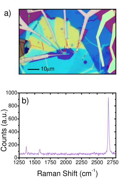
The optical image of the device presented in the main text is shown in Figure S1a. Graphene is made using the exfoliation method(Novoselov et al., 2005), prior to encapsulation in hexagonal boron-nitride (hBN) the graphene is verified to be single layer using Raman spectroscopyFerrari et al. (2006). The measured Raman spectrum is shown in Figure S1b. An AFM image is taken of the completed hBN-graphene-hBN stack (not shown), and an area free of bubbles and defects is chosen for further processing. Using CHF3/O2 plasma, the hBN-Grahpene-hBN stack is etched thorough in order to make quasi-one dimensional electrical contacts with superconducting electrodes(Amet et al., 2016). Molybdenum-Rhenium(MoRe) alloy electrodes are deposited onto the device using DC sputtering with the approximate thickness of nm. The MoRe contacts define the Josephson junction dimensions. However, the MoRe leads are terminated past the active area of the device. (Green arrow in Figure S1a). The bonding pads and thin metal leads making contact to MoRe are made of Cr/Au (nm/nm). This interface between the MoRe and the Cr/Au portion of the contacts results in a resistance that isolates the Josephson junction from the effect of the parasitic capacitance between the bonding pads(Vion et al., 1996; Borzenets et al., 2013)
Switching current dependence on Temperature
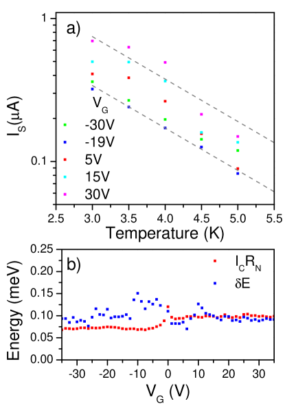
In Josephson junctions, the measured switching current is suppressed from the expected maximum critical current , with found to be decreasing with increasing temperature (Tinkham, 2004). Measuring the trend of with respect to temperature , one can determine whether the junction is in the diffusive(Ke et al., 2016; Dubos et al., 2001a, b) or ballistic transport regime(Kulik, 1969; Bardeen and Johnson, 1972; Svidzinskiǐ et al., 1972; Svidzinsky et al., 1973; Beenakker, 1992; Beenakker and van Houten, 1991; Lee et al., 2015; Borzenets et al., 2016a). Additionally, by sweeping gate voltage , one can also determine whether the junction is made of single layer or multi-layer graphene. For the case of a Josephson junction governed by ballistic electron transport, and with junction length (the superconducting coherence length) we expect that (Kulik, 1969; Bardeen and Johnson, 1972; Svidzinskiǐ et al., 1972; Svidzinsky et al., 1973; Borzenets et al., 2016a). The value is related to the Andreev Bound States energy level spacing ()Kulik (1969); Bardeen and Johnson (1972); Svidzinskii (1982); Tinkham (2004); Golubov et al. (2004). Here is the the Fermi velocity; and in single layer graphene is a constant with respect to carrier density. Therefore, is expected to be independent of the applied gate voltage (as long as the junction remains ballistic). The trend of the switching current versus temperature can be seen in Figure S2a, plotted on a semi-log scale for several values of . A nearly linear decay can be observed. Fitting the data to the above exponential dependence, we can extract the value of .The guidelines of the fit result are shown as dashed lines in Figure S2a, while the fitted value of is presented in Figure S2b. One can see that is independent with respect to gate voltage (aside from the expected deviations close to the Dirac point). Moreover, the extracted value is consistent with the designed length of the junction(Borzenets et al., 2016a). As the temperature approaches zero, the switching current approaches the critical current with . (Here is the normal resistance.) It has been found empirically, that the dimensionless proportionality constant is , and is suppressed by the coefficient of transmission across the junction(Borzenets et al., 2016a). In Figure S2b, alongside , we plot the value of . The critical current is back calculated from the fitted Josephson energy in the main text. Indeed, we find a good match between the two values. This suggests that our device is single layer graphene, and is governed by ballistic electron transport. Moreover, that our fitted Josephson energy is close to the actual of the device.
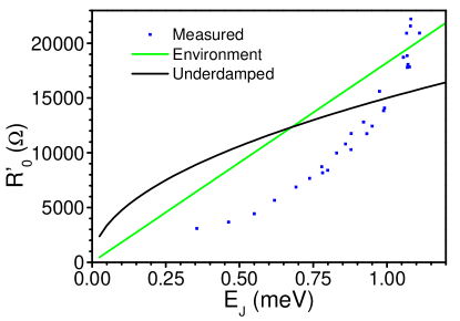
Comparisson to Underdamped and Damped by Environment regimes
The main text presents the analysis of phase diffusion in the overdamped regime. Here we follow the analyses as if the Josephson junction was underdamped, or damped by the environment at the plasma frequency. In following previous works, define the prefactor to the exponential in the main text Equation 1 as a variable with (Borzenets et al., 2011). For underdamped junctions, (Kautz and Martinis, 1990), where is the plasma frequency. Note that is the capacitance of the junction, and is a constant.) However, if the junction is underdamped at low frequencies, but becomes overdamped at the plasma frequency (due to being shorted by the environment), we have (Ingold et al., 1994). Here is the real part of the high frequency impedance caused by the junction’s environment (Ingold et al., 1994). Typically is found to be , and can also be treated as a constant. (Note, that the above relationship holds only for Ingold et al. (1994)). The measured versus the Josephson energy is shown in Figure S3 (data taken at 4.0K). Alongside, we plot the best fitting results obtained for each of the two cases mentioned above. Note that the trend of the measured result is super-linear; while the expected trend for the underdamped case is a square root dependence, and a linear trend is expected in the damped by the environment case. Clearly, the above two analyses do not apply. It is important to note that Ref. Borzenets et al., 2011, erroneously used the same analysis via the variable for the overdamped case. This is not correct as the exponential dependence only approximates the slope of the trend with respect to temperature, not the absolute value(Tinkham, 2004; Ambegaokar and Halperin, 1969). Instead, the full expression from Ref. Ambegaokar and Halperin, 1969 is to be used; as was done in the main text.