Origin of Irradiation Synergistic Effects in Silicon Bipolar Transistors: a Review
Abstract
The practical damage of silicon bipolar devices subjected to mixed ionization and displacement irradiations is usually evaluated by the sum of separated ionization and displacement damages. However, recent experiments show clear difference between the practical and summed damages, indicating significant irradiation synergistic effects (ISEs). Understanding the behaviors and mechanisms of ISEs is essential to predict the practical damages. In this work, we first make a brief review on the state of the art, critically emphasizing on the difficulty encountered in previous models to understand the dose rate dependence of the ISEs. We then introduce in detail our models explaining this basic phenomenon, which can be described as follows. Firstly, we show our experimental works on PNP and NPN transistors. A variable neutron fluence and -ray dose setup is adopted. Fluence-dependent ‘tick’-like and sublinear dose profiles are observed for PNP and NPN transistors, respectively. Secondly, we describe our theoretical investigations on the positive ISE in NPN transistors. We propose an atomistic model of transformation and annihilation of displacement-irradiation-induced defects in p-type silicon under ionization irradiation, which is totally different from the traditional picture of Coulomb interaction of oxide trapped charges in silica on charge carriers in irradiated silicon. The predicted novel dose and fluence dependences are fully verified by the experimental data. Thirdly, the mechanism of the observed negative ISE in PNP transistors is investigated in a similar way as in the NPN transistor case. The difference is that in n-type silicon, displacement-irradiation-induced VO defects also undergo an ionization-induced transformation and annihilation process. Our results show that, the evolution of displacement defects due to carrier-enhanced defect diffusion and reaction is the dominating mechanism of the ISEs. Finally, we give a perspective on future investigations on the ISEs when the displacement and ionization irradiations are present simultaneously.
I Introduction
Irradiation synergistic effect. Silicon (Si)-based NPN and PNP transistors are building blocks of modern microelectronics, such as operational amplifiers and voltage comparators. When these devices are used in outer space and other extreme environments such as nuclear reactors, both charge carriers and atomic displacements will be generated in the silica and silicon materials, which result in ionization and displacement damages in the devices. Oldham and McLean (2003); Srour et al. (2003) Conventionally, the practical damage is usually assumed as a simple sum of the ionization damage (ID) and displacement damage (DD), which then can be evaluated individually at ground by carrying out -ray and neutron irradiation experiments, respectively. The primary reason for the separability of the damages is that, the ID is caused by the ionization defects, oxide trapped charges (OTs) and interface traps (ITs), generated in the silica and near interface, Dressendorfer (1998) while the DD is caused by the displacement defects, such as divacancies (V2) and vacancy-oxygen complex (VO), generated in Si. Fleming et al. (2010) Accordingly, it was widely and always believed that there is no direct interaction between these two irradiation-induced defect dynamics and the practical damage can be separated.
However, in recent experiments it has been clearly demonstrated that, when these bipolar transistors are simultaneously or subsequently irradiated by displacement and ionization irradiations, the practical damage is usually smaller or larger than the simply summed damage. Barnaby et al. (2001, 2002); Gorelick et al. (2004); Li et al. (2012a, b, 2015); Wang et al. (2016); Song et al. (2019, 2020a) These phenomena can be called as irradiation synergistic effects (ISEs), which are negative in PNP transistors and positive in NPN transistors, respectively. The presence of ISEs imply that one cannot evaluate the practical damage by carrying out separated neutron and -ray irradiations and simply summing the damages up. To obtain a relatively true damage, one must know the behaviors of the ISEs and understand the underlying mechanisms.

Existing model of the ISEs. Currently, the ISEs are explained in a point of view of interfacial interaction in the device scale, see, Fig. 1. Especially, the effect is believed to stem from the Coulomb interaction of OTs in the silica layer on the charge distributions in the displacement-damaged silicon base region, where the non-radiative Shockley-Read-Hall (SRH) carrier recombination occurs. Barnaby et al. (2001, 2002) To be fair, this point of view is rather natural: the outcomes of the ID and DD are the ionization and displacement defects in the silica layer and silicon region, respectively, so, intuitively, the synergistic effect of the ID and DD should come from the Coulomb interaction between the charged defects and carriers in these two different regions. Actually, the opposite signs of the ISEs in NPN (which is ) and PNP (which is ) transistors can be consistently explained by this mechanism, as followings. A positive ISE arises in NPN transistors because the positively charged OTs repel the positively charged holes as majority carriers near the surface of the p-type silicon base, which reduces the difference of hole and electron densities and enhances the SRH recombination current in the base region, see Fig. 1(a). On the contrary, a negative ISE would arise in PNP transistors because the positive OTs attract the negatively charged electrons as majority carriers near the surface of the n-type silicon base, which widens the difference of carrier densities and thus suppresses the SRH recombination in the base region, see Fig. 1 (b).
Difficulty of the existing model in understanding the ISE. However, we notice that some of the experimental observations of the ISEs cannot be explained by the existing mechanisms. The most remarkable feature is the dose-rate dependence of the effect. According to a reduced high-dose-rate sensitivity, Pease et al. (2008) the OTs will become fewer for decreasing dose rate irradiation at a fixed total dose. Song et al. (2020b) According to the Coulomb interaction mechanism, the ISE should become weaker as the dose rate decreases. However, this deduction is totally opposite to the experimental results, where the synergistic effects between DD and ID are found to be enhanced at lower dose rate -ray irradiations. Song et al. (2019, 2020a) On the other hand, the ionization dose (dose rate) and displacement fluence/flux dependencies of the ISEs are essential for the understanding and modeling. However, existing experimental works usually use proton and electron irradiations, where the simultaneously generated DD and ID are hard to separate. Barnaby et al. (2001); Li et al. (2010) Meanwhile, existing investigations usually consider fixed ionization dose or displacement fluence. So, till now, the behavior of the ISEs as functions of the ionization dose, dose rate, and displacement fluence is still not clear.
To sum up, the ISEs are important to evaluate practical damages of silicon bipolar transistors in irradiation environments. However, there are still huge gaps in the investigations of the behaviors and mechanisms of the effects. The behavior of the ISEs is far from clear due to the fixed displacement fluence and/or ionization dose in existing experiments. The understanding of the effect is based on a point of view of an interfacial interaction, which seems natural but cannot explain the dose rate dependence of the effect. Thus, new experimental studies and mechanisms that can self-consistently describe the experimental observations are urgently needed.


II Behaviors of the ISEs
II.1 Experimental setup to explore the behaviors
To explore the behavior of the ISEs in PNP and NPN transistors, Song et al. (2019, 2020a) LM324N chips with 4 PNP-type input-stage transistors in each chip and 3DK9D NPN-type transistors were selected as the research object, respectively. These devices were chosen because they are sensitive to both ID and DD. The neutron irradiation hardly influences the dynamics of OTs in the oxide layer, Raymond and Petersen (1987) hence, we adopt a sequential neutron/-ray irradiation configuration. The processes of the sequential irradiation experiments for PNP transistors is shown in Fig. 2 (a). The transistors are first irradiated by neutron to the fluence as indicated in the figure along the vertical direction; then they are irradiated by -ray to the dose as indicated in the figure along the horizontal direction. By these irradiations the practical damages can be obtained. The summed damages as a reference are obtained by another two pure -ray irradiations. For each neutron--ray condition, 8 PNP transistors (within 2 chips) are used to avoid possible misjudgment due to sample variability. Note, existing experiments Barnaby et al. (2001); Gorelick et al. (2004); Li et al. (2012a); Wang et al. (2016) usually adopt only a fixed displacement fluence and ionization dose, hence is very different from the present experimental setup. The radiation sources, irradiation bias, and testing systems are described in detail in Ref. Song et al., 2019. The ISE of NPN transistors is investigated by a very similar sequential neurton/-ray irradiation experiment, which is shown in Fig. 2 (b) and has been described in detail in Ref. Song et al., 2020a.

II.2 Fluence-dependent ‘tick’-like dose curves of PNP transistors
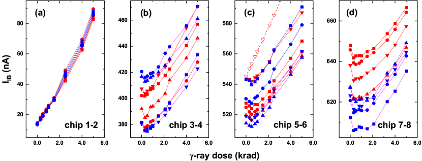
Artificial summed damages. The individual DDs of the PNP transistors are shown in Fig. 3, from which a sub-linear dependence of the input bias current () on the neutron fluence is clearly seen. It is also seen that, the DDs of the 8 transistors under a same fluence are different due to sample-to-sample variability. To obtain the artificial summed damages, Nos. 1-2 and 9-10 chips were irradiated by a low and high dose rate rays, respectively. The results for the former are displayed in Fig. 4 (a). An almost linear increase of the ID is seen and an average slope of nA/krad(Si) and nA/krad(Si) is extracted for the low and high dose rate case, respectively. The summed damage reads:
| (1) |
where is the initial DD before -ray irradiations. A typical result is plotted in Fig. 4 (c) as the dashed line.


Practical damages and behavior of the negative ISE. The -ray response of the - chips at low dose rate with different ’s are displayed in Figs. 4 (b)-(d). It is seen that, the practical damages of all 24 transistors are smaller than their corresponding summed damages. This means that we obtain a clear negative ISE in PNP transistors. Remarkably, the practical damages display ‘tick’-like curves: the input-bias currents first exponentially decrease for relatively small -ray dose and then linearly increase for relatively large -ray dose. Moreover, the slope of the linear increase is obviously smaller than that of the pure ID, . The - chips display similar negative ISEs at high dose rate -ray irradiations, see Ref. Song et al., 2019. To further obtain the and -ray dose rate dependences of the ISE, we plot six typical curves in Fig. 5, from which we can see that, the exponential decay of the practical damage at small -ray dose becomes stronger when the dose rate decreases; while the decrease of the slope at large -ray dose becomes bigger when the initial DD increases. These regular behaviors, especially the dose rate dependence of the ISE, cannot be explained by the traditional Coulomb interaction mechanism.
II.3 Fluence-dependent sublinear dose curves of NPN transistors
The practical neutron/-ray damage (the base currents) of the 3DK9D NPN transistors are shown in Fig. 6 (a) as a function of the -ray dose at a dose rate of 10 rad/s (see the dots). Besides, the summed damages for three typical samples are obtained from a direct sum of their DDs and the average ID of five extra samples (see the dashed curves). From the results it is clear that a positive ISE arises for the NPN transistors. From Fig. 6 (a) it is also seen that, the practical damages increase sublinearly as the ionization dose increases; meanwhile, the positive ISE becomes larger when the initial DD increases. The practical and summed damages are shown in Fig. 6 (b) for the low dose rate (10mrad/s) case. A second stage arises when the dose exceeds 2 krad. However, the two different stages are found to show similar dependences on the -ray dose and neutron fluence as the high dose rate case.
To sum up, we have designed a variable neutron-fluence and -ray-dose irradiation experiment to explore the behaviors of the negative and positive ISEs in PNP and NPN transistors. The results show that both ISEs display regular dependences on the -ray dose, dose rate, and neutron fluence. The obtained features are quite different for PNP and NPN transistors.
III Mechanism and analytical model of the positive ISE in NPN transistors
In all previous works, Barnaby et al. (2001, 2002); Li et al. (2012a, b, 2015) the ISEs were attributed to the influence of the positively charged OTs accumulated in silica on the charge density in irradiation damaged silicon, see Fig. 1 (a) for NPN transistors and (b) for PNP transistors, respectively. The different polarity of the ISE in PNP and NPN transistors could be explained by this mechanism. However, as indicated above, the dose rate dependence of the effect cannot be explained by the Coulomb interaction mechanism. Besides, the above obtained ‘tick’-like and sublinear dose dependence of PNP and NPN transistors, respectively, and their strong fluence dependence are also hard to understand from the theory. These behaviors imply that a new underlying mechanism for the ISEs in silicon bipolar transistors should be developed.
We have systematically investigated this basic phenomena from the point of view of ionization-irradiation-induced evolution of displacement defects in Si. Song et al. (2020a, 2019) The primary consideration is that, the amplitude of the SRH recombination current in the bipolar transistors is in direct proportion to the concentration of the displacement defects in Si; while these defects can evolve under ionization irradiation, due to carrier-enhanced defect diffusion Kimerling et al. (1975); Kimerling (1976); Bar-Yam and Joannopoulos (1984a, b); Baraff and Schlüter (1984); Car et al. (1984) and recombination-enhanced defect reactions. Lang and Kimerling (1974); Weeks et al. (1975); Kimerling (1978) The diffusion of displacement defects in Si can be enhanced by alternating capture and lose the ionization-irradiation-induced electrons. Bar-Yam and Joannopoulos (1984a, b); Baraff and Schlüter (1984); Car et al. (1984) On the other hand, the defect reactions can be enhanced by energy liberated upon non-radiative recombination. Weeks et al. (1975) In p-type silicon, is the only neutron-induced active defect, while in n-type silicon, both and VO are neutron-induced active defects, see Fig. 7 (a). In this section, we will first introduce the simpler case, i.e., the understanding and modeling of the ISE in NPN transistors with p-type silicon as the channel. Song et al. (2020a) Then in the next section we further introduce the case of PNP transistors with n-type silicon as the channel. Song et al. (2019)

The defect dynamics in p-type silicon under consideration is a -ray induced transformation reaction from to divacancy-oxygen complex () and a -ray induced annihilation reaction between and self-interstitials (), Song et al. (2020a) see the bottom half of Fig. 7 (a). Based on these mechanisms, we first derive an analytical model of the defect concentrations as a function of the -ray dose and neutron fluence (Sec. III A). Then we relate the defect concentrations to the base current of the NPN transistors to obtain a model for the ISE (Sec. III B). We at last test the proposed model through the variable-dose and -fluence data as shown in Sec. II C (Sec. III C).
III.1 Defect evolution model in p-type silicon
As identified by Deep Level Transient Spectroscopy (DLTS), Lang (1974a, b) the main defect type in neutron irradiated p-type silicon is donor-like divacancies (), Cheng et al. (1966); Lee and Corbett (1976); Lindström et al. (1999) see Fig. 7 (a). We notice that, the diffusion of will be greatly enhanced when the damaged Si samples are further subjected to a -ray irradiation. Song et al. (2020a) The microscopic picture of such a carrier-enhanced defect diffusion is as followings. The -ray-induced charge carriers will shift the quasi-Fermi energy in the Si samples. Accordingly, the defects can change from one charge state at its equilibrium site to another that is not at equilibrium. Bar-Yam and Joannopoulos (1984a, b); Baraff and Schlüter (1984); Car et al. (1984) The latter will easily diffuse to its equilibrium site without having to overcome a diffusion barrier. These behaviors largely enhance the diffusion of defect. Besides, many oxygen interstitials (), which are electrically-inactive, have been introduced in the Si sample in its growth process. The moving defects will be trapped by where they react to form another defect that is electrically-active, Mikelsen et al. (2005); Markevich et al. (2014)
| (2a) | |||
| see Fig. 7 (a). | |||
On the other hand, the energy liberated upon nonradiative recombination will be converted into vibrational energy that can be utilized to promote the defect reactions, which include the dissociation of clusters and re-emission of self-interstitials in damaged Si. Lang and Kimerling (1974); Weeks et al. (1975); Kimerling (1978) The charge-enhanced defect diffusion also applies to the emitted self-interstitials. The moving divacancies and self-interstitials can collide and annihilate each other Song et al. (2020a)
| (2b) |
The rate equation of can be derived from Eq. (2). The result is , where and are the transformation and annihilation reaction velocities in Eqs. (2a) and Eq. (2b), respectively, see Fig. 7 (a). To simplify the calculations, we replace and in the last term by their initial concentrations, which are directly related to the irradiation fluence of neutron, . This replacement can be done because the annihilation rate is relatively small Mikelsen et al. (2005); Markevich et al. (2014) and the concentration of is directly proportion to the total amount of vacancies. The above equation becomes
| (3a) | |||
| where and are effective transformation and annihilation velocities. The accompanying rate equation for defects reads | |||
| (3b) | |||
The initial conditions for the two defects are and . Solving the resulting coupled equations with these conditions, we obtain the -ray dose dependence of the concentration of and
| (4a) | |||
| (4b) |
Here we have changed to , where is the dose rate. From the pair of solutions it is clear that, the concentration of is an exponential decay function of the -ray dose, while the concentration of is both an asymptotic growth function and a linear decay behavior of the -ray dose. Song et al. (2020a) The neutron fluence dependence of the defect concentrations is indicated by the factor in Eq. (4). Song et al. (2020a)
Comparison with the annealing experiments. Evolution of displacement defects also happens in traditional annealing process induced by elevated temperature. However, the self-interstitial emission mechanism described in Eq. 2 (b) is absent for this case, Kimerling (1978); Pellegrino et al. (2001) as the energy is not enough to decompose the clusters. As a result, the defect evolution is only due to defect diffusion and transformation induced by elevated temperatures, as described by Eq. (2a). Then, the defect concentrations as a function of the annealing time () reduces to
| (5a) | |||
| (5b) |
These results are the same as those in Ref. Mikelsen et al., 2005. It is noticed that, here the increase of equals exactly to the decrease of , and we will not observe a linear decay term of the defect concentration as described in Eq. (4b).
III.2 Recombination current model of NPN transistors
To show the behavior of the ISE in NPN transistors, we relate the defect concentrations in p-type Si to the SRH base current in the NPN transistor, which are found to be in direct proportion to each other. Pierret and Neudeck (1987); Adell and Boch (2014) The donor levels of the defects in p-type Si have been identified by DLTS. Mikelsen et al. (2005); Markevich et al. (2014) As shown in Fig. 7 (a), there is one active donor level for the defect, at eV, and two active donor levels for the -ray induced defect, at eV and at eV. The contribution factors of each defect charge state to the base current can be denoted as , , and , see Fig. 7 (a). Note, the same contribution factor of is often assumed Ganagona et al. (2014) as and have almost the same donor levels and hole capture cross sections. Srour et al. (1973); Myers et al. (2008); Liu et al. (2015) The -ray-induced changes of the base current corresponding to the evolution of defects in Eq. (4) read Song et al. (2020a)
| (6a) | |||
| (6b) | |||
| (6c) |
Here the measurable initial DD due to the neutron-irradiation-induced is denoted as , the ratio between the -ray-irradiation-induced annihilation and transformation velocities is denoted as , is a characteristic dose of the transformation from to , and is a ratio between the contribution factors of the first and second donor levels of . The total change of the base current is the sum of the above three components, which reads Song et al. (2020a)
| (7) |
This is the desired analytical model of the positive ISE in NPN transistors, which is based on the ionization-irradiation-induced dynamics of displacement defects in p-type silicon and shows the explicit dependence of the applied -ray dose and initial DD (neutron fluence). These four current profiles are plotted in Fig. 7(b) by using different colors.
The derived model predicts that, the positive ISE of NPN transistors would possess one asymptotic growth term and one linear decay term as a function of the -ray dose, Song et al. (2020a) see the black curves in Fig. 7 (b). The asymptotic growth term of the ISE stems from the ionization-irradiation-induced asymptotic growth of the defect, see the magenta solid curves in Fig. 7 (b). The linear decay term of the ISE results from the two ionization-irradiation-induced linear decaying components of and , see the blue and magenta straight solid lines in Fig. 7 (b). As shown by the red and blue dashed curves in Fig. 7 (b), the remaining asymptotic growth of and the exponential decay of cancel each other. The reason is the one-to-one transformation between and defects and the same contribution factors of their first donor levels. The proposed model also predicts an almost linear dependence of the magnitude of the asymptotic growth term on the initial DD (), and a quadratic dependence of the slope of the linear decay term on the initial DD. Song et al. (2020a) The reasons are the one-to-one correspondence between and in the transformation and the binary behavior of interstitials and vacancies in the annihilation. Song et al. (2020a) The proposed defect dynamics model also predicts a dose-rate dependence of the two independent synergistic terms.

III.3 Experimental verification and parameter extraction of the model of NPN transistors
To testify the above proposed model for NPN transistors, we try to fit the obtained data in Sec. II.C. by using a fitting model
| (8) |
where denotes the sample index. The first term in the fitting model contains both the linear decay term in the proposed physical model and the IDs of the samples. As the ID varies among different samples, the physical model, Eq. (7), cannot be directly used. In stead, the presence of the linear decay term can be identified by the statistical difference between the extracted and (the slopes of pure ID). The correspondence between the fitting and physical parameters is . The second term in the fitting model is exactly the asymptotic growth term in the proposed physical model. The correspondence between the parameters is and . The fitting curves for the high dose rate case are plotted in Fig. 6 (a), which are found to work very well for all 9 samples. The separated linear component (blue dashed) and asymptotic growth term (red dashed) of a typical sample are shown in Fig. 8 (a). A significant decrease is found in the linear component relative to the average slope of pure ID (black dashed). For all 9 samples’ statistical results, see plotted in Fig. 9 (a). Similar perfect fitting can be done for the low dose rate case within the first stage, see the fitting curves plotted in Fig. 6 (b). These facts verify the predicted asymptotic growth and linear decay terms in the ISE of NPN transistors, reflecting the proper underlying defect evolution physics in the prediction of dose dependence of the ISE.
To further testify the initial DD dependence of the proposed model, we plot the fitting parameters of Eq. (8) (, , and ) in Fig. 9 as a function of the base current. A decreasing trend is found in Fig. 9 (a) for the slope of the linear term as a function of the initial DD, , which starts from the pre-irradiation base current, . Further investigation shows that a quadratic dependence is satisfied, i.e., . This behavior is consistent with the model’s prediction. Calculations show that and for the high and low dose rate -ray irradiation, respectively. A linearly increasing trend is found in Fig. 9 (b) for the amplitude of the asymptotic growth term as a function of the initial DD. This feature is also the same as the prediction of the model. The characteristic dose of the asymptotic growth term shown in Fig. 9 (c) is insensitive to the DD. These results further confirm the novel initial DD dependence predicted by the proposed model, reflecting the proper defect evolution physics underlying the model.
The significant difference between the red and blue dots in Fig. 9 also reflect the predicted dose-rate dependence of the ISE. For a fixed total dose, the carrier-enhanced defect diffusion and recombination-enhanced defect reactions become stronger for decreasing dose rate, which means dramatically increased action time. This fact readily explains the dose rate dependence of the ISE in NPN transistors, which, however, cannot be explained by the Coulomb interaction mechanism.
The physical parameters in Eq. (7) can be calculated from their correspondence to the fitting parameters. The results are shown in Table 1 and some valuable facts can be inferred. The values of at different dose rates indicate that the second donor level of contributes 5 or 10 times less than the first donor level of and . The values of implies that , which supports in Eq. (7) hence the linear dependence of the growth term on the initial DD. The dose rate sensitivity of both the dynamic parameters ( and ) and the contribution factor () of the defects result in the dose rate dependence of the ISE.
| dose rate | |||
|---|---|---|---|
| 10 mrad/s | 0.23 | 0.26 | |
| 10 rad/s | 0.11 | 0.38 |
IV Mechanism and analytical model of the negative ISE in PNP transistors
As discussed in Sec. II B, a negative ISE is observed for PNP transistors. The practical neutron--ray damage displays an interesting fluence-dependent ‘tick’-like dose curve. In this section this effect will be understood and modeled in a similar way as that for the NPN transistors. Note that, in n-type silicon, both and VO are neutron-irradiation-induced active defects.
IV.1 ISE due to the evolution of in n-type silicon
Similar to the p-type silicon case, in n-type silicon as acceptor levels will transform to due to the above mentioned carrier-enhanced diffusion of under the -ray irradiation, Kimerling et al. (1975); Kimerling (1976); Bar-Yam and Joannopoulos (1984a, b); Baraff and Schlüter (1984); Car et al. (1984) see Fig. 7 (a). will also be annihilated by self-interstitials which are emitted due to recombination-enhanced defect reactions. Lang and Kimerling (1974); Weeks et al. (1975); Kimerling (1978) The ionization dose and neutron fluence dependence of the concentrations of and are given by Eq. (4).
Different from the p-type silicon case, both and in n-type silicon have two acceptor levels: at , at , at , and at , Mikelsen et al. (2005) see the upper half in Fig. 7 (a). Denoting the contribution factors of these acceptor charge states to the base current of PNP transistors as , , , and , respectively. Note, the same contribution factor of () can be assumed, because and ( and ) have almost the same acceptor levels and electron capture cross sections. Mikelsen et al. (2005) Multiplying the defect concentrations, Eq. (4), by these factors, we obtain the corresponding components of the base current in PNP transistors, which are plotted as the red and blue profiles in Fig. 7 (c). As the exponential decay curve of () and the asymptotic growth curve of () cancel each other, we can find that the net result due to the ionization-induced evolution of displacement defects in n-type Si is a linear decay term of the ISE in PNP transistors
| (9) |
Here is the measurable initial DD due to in PNP transistors and is the ratio between the annihilation and transformation reactions for in n-type silicon; these factors are different from the and factors in Eq. (7) for NPN transistors.
IV.2 ISE due to the evolution of VO in n-type silicon
Different from p-type silicon, neutron-irradiation-induced VO is also an effective recombination center in n-type silicon, see the upper half in Fig. 7 (a). So, besides the -ray-irradiation-induced evolution of VO should also be considered for PNP transistors. Due to the above mentioned carrier-enhanced diffusion of Kimerling et al. (1975); Kimerling (1976); Bar-Yam and Joannopoulos (1984a, b); Baraff and Schlüter (1984); Car et al. (1984) and recombination-enhanced emission of self-interstitial, Lang and Kimerling (1974); Weeks et al. (1975); Kimerling (1978) the transformation and annihilation reactions of VO will happen
| (10a) | |||
| (10b) |
According to Ref. Pellegrino et al., 2001, the transformation reaction happens because the moving VO will be trapped by electrically-inactive , which forms an electrically non-active defect , see Fig. 7(a). The annihilation reaction happens because the moving vacancy-oxygen complex and self-interstitials can collide and generates electrically-inactive . Eqs. (2) and (10) make up the full defect dynamics accounting for the negative ISE in PNP transistors.
Using the same modeling approach as and in Sec. III B, the concentrations of VO and can be obtained as functions of the -ray dose and initial DD
| (11a) | |||
| (11b) |
Here and are effective reaction velocities of the transformation and annihilation processes of the defects in n-type Si, respectively, see Fig. 7 (a). The used initial conditions are and . The results indicate that, similar to the defect, the concentration of VO will exponentially decay under ionization irradiation, and similar to defect, the concentration of will asymptotically increase and linearly decay as a function of the -ray dose.
The faded VO defect contributes an acceptor level Svensson et al. (1991) and the generated defect is non-active in n-type silicon. Denoting the contributing factor of VO to the recombination current as , see Fig. 7 (a). The base current in PNP transistors due to VO and can be solved as a function of the -ray dose and initial DD. The net effect is found as an exponential decay of the initial base current () contributed by VO
| (12) |
see the magenta curve in Fig. 7 (c). Here is the measurable initial DD due to VO defect, is the rate ratio between the annihilation and transformation reactions of VO in Si, and is a characteristic dose of the transformation reaction of VO in Si.
Summing up Eqs. (9) and (12), we at last obtain the defect dynamics model for the negative ISE of the base current in PNP transistors
| (13) |
see the black curves in Fig. 7 (c).
Eq. (13) predicts that, there would be two independent terms in the ISEs of the PNP transistors: one linear decay term depending on the -ray dose, which stems from the ionization-irradiation-induced transformation and annihilation of in n-type silicon; and one exponential decay term depending on the -ray dose, which stems from the ionization-irradiation-induced transformation and annihilation of VO in n-type silicon. Eq. (13) also predicts an almost linear dependence of the amplitude of the exponential decay on the initial DD due to VO () and a quadratic dependence of the slope of the linear decay term on the initial DD due to (). Eq. (13) also predicts a dose rate dependence of both terms of the ISE.

IV.3 Experimental verification of the model of PNP transistors
Following a similar way as the NPN transistor case (Sec. III C), the proposed model, Eq. (13), is testified by the data of PNP devices displayed in Sec. II.B. The fitting model is
| (14) |
Again, the first term in the fitting model contains both the linear decay term in the proposed physical model and the unknown linear ID; the presence of the linear decay term can be identified by the statistical difference between and . The correspondence between the fitting parameters in Eq. (14) and physical parameters in Eq. (13) is . The second term in Eq. (14) is exactly the exponential decay term in Eq. (13). The correspondence between the parameters are and . It is noted that is exactly the initial base current due to the VO defects. The fitting profiles are plotted in Fig. 5 as solid curves, which are found to work very well for all samples. The dashed curves in Fig. 8 (b) show the linear component and the exponential decay term of a typical fitting curve of the PNP device. A significant decrease is found for the linear component (blue dashed) with respect to the average slope of pure ID (black dashed). These facts verify the predicted linear and exponential decay terms in the ISE of PNP transistors, reflecting the proper defect evolution physics in the prediction of the dose dependence of the ISE in PNP transistors.
The fitting parameters and are plotted in Figure 10 as a function of the base current, to further testify the initial DD dependence of the proposed model. containing the initial DD (). The fitting characteristic dose () is not sensitive to the initial DD, and is 0.47 krad and 0.50 krad for the low and high dose rates, respectively. Note, these values are larger than those for the defects as shown in tab. 1, reflecting a slower transformation process for VO defects in Si. The data of high dose rate with the neutron fluence of is of low quality and are excluded from the fitting process. It is clear from Fig. 10 (b) that, the amplitude of the exponential decay term, , shows an almost linear dependence on the initial DD, which is started from the pre-irradiation base currents, , see the dashed guide lines. This dependence is consistent with the prediction of the proposed model. It is also found that for the low (high) dose rate -ray irradiation, the value of is only 1/38 (1/170) of the initial DD, . This fact implies that the neutron-induced (annealable) VO defects are much fewer than the neutron-induced defects. As can be seen in Fig. 10 (a), the slope of the linear term decreases as the initial DD increases. A quadratic dependence is found for the overall trend, . Since is much smaller than , this result means , which is also consistent with the model’s prediction. The value of is for both low and high dose rates. The above results further verify the predicted initial DD dependence of the ISE in the proposed model, reflecting the proper physics of defect evolution underlying the model.
The significant difference between the red and blue dots in Fig. 10 reflects the dose-rate dependence of the ISE predicted by the model. The reason is that the ionization-induced defect transformation and annihilation becomes stronger for lower dose rate irradiation. This fact readily explains the dose rate dependence of the ISE in PNP transistors, which cannot be explained by the Coulomb interaction mechanism. Different from the NPN transistor case, the physical parameters cannot be calculated from the fitting parameters.
V Perspective
Several important works should be carried out in future investigations on the ISEs of silicon bipolar transistors. The first is the DLTS characterization of the ionization-irradiation-induced evolution of the displacement defects in n-type and p-type silicon, which can provide direct evidences for the atomistic mechanisms of the ISEs. The second is the explicit dose rate dependence of the ISEs, from which the nature of the two underlying mechanisms, i.e., carrier-enhanced defect diffusion and recombination-enhanced defect reactions, can be further explored. The third and last is the behavior and mechanism of ISE due to simultaneous displacement and ionization irradiations. The displacement defect dynamics contains processes of fast generation, short-term annealing, and long-term annealing of displacement defects. Srour et al. (2003) The above results show that the displacement defects during or after the long-term annealing process can be strongly modified by ionization irradiations. When the transistors are subjected to simultaneous displacement and ionization irradiations, which is the usual cases, the ionization irradiation can further dramatically alter the short-term annealing of displacement defects. Gregory and Sander (1967) The behavior and mechanism of such a simultaneous ISE should be an important research subject for both basic researches and practical applications.
VI Conclusion
In summary, the irradiation synergistic effect (ISE) is an important physical phenomenon to understand and predict the practical damages of semiconductor devices from the individual displacement and ionization irradiation experiments. In this work, we have made a concise review on the current investigation status of the effect in silicon bipolar transistors. We want to emphasize that, the existing experimental studies of the behavior of the effect are usually limited to fixed displacement fluence and/or fixed ionization dose, while the previous theoretical model encounters physical troubles to explain the dose rate dependence of the ISE.
Here, we describe in detail our recent investigations of the behavior of the effect and introduce our new mechanism of the effect. Our experimental investigation uses a variable-fluence and dose neutron/-ray irradiation setup as well as a large sample size to explore the behavior of the ISE. Our theoretical investigation adopts a point of view of ionization-irradiation-induced evolution of displacement defects in Si, that is totally different from the Coulomb interaction mechanism in previous works. We demonstrate that both the positive and negative ISEs in NPN and PNP transistors can be fully and self-consistently explained by the same basic mechanism, i.e., the ionization-irradiation-induced transformation and annihilation of the displacement-irradiation-induced defects in silicon. However, as the electrically-active displacement defects and their transformation products are different for p-type and n-type silicon, the ISEs of NPN and PNP transistors show quite different behaviors. Specifically, the ionization-driven transformation and annihilation of active defect in p-type silicon give arises to a positive ISE in NPN transistors containing an asymptotic growth and a linear decay term; the same processes of both active and VO defects in n-type silicon give arises to a negative ISE in PNP transistors containing a linear and exponential decay terms. Both ISEs show a regular dependence on the initial displacement damage of the bipolar transistors, which can also be self-consistently explained by the defect evolution mechanism. The dose rate problem encountered by the previous Coulomb interaction mechanism can be naturally explained by the present model.
We believe that the uncovered behavior and mechanism of the ISEs will be helpful to predict the practical damage of silicon bipolar transistors. The developed experimental and modeling methods in our works can be extended to the investigation of ISEs in other semiconducting materials and devices.
Acknowledgments
This work was supported by the Science Challenge Project under Grant No. TZ2016003-1 and National Natural Science Foundation of China (NSFC) under Grant Nos. 51672023; 11634003; U1930402; 11404300.
References
- Oldham and McLean (2003) T. R. Oldham and F. McLean, IEEE transactions on nuclear science 50, 483 (2003).
- Srour et al. (2003) J. Srour, C. J. Marshall, and P. W. Marshall, IEEE Transactions on Nuclear Science 50, 653 (2003).
- Dressendorfer (1998) P. V. Dressendorfer, Basic Mechanisms for the New Millennium, Tech. Rep. (Sandia National Labs., Albuquerque, NM (United States), 1998).
- Fleming et al. (2010) R. M. Fleming, C. Seager, D. Lang, and J. Campbell, Journal of Applied Physics 108, 063716 (2010).
- Barnaby et al. (2001) H. J. Barnaby, R. D. Schrimpf, A. L. Sternberg, V. Berthe, C. R. Cirba, and R. L. Pease, IEEE Transactions on Nuclear Science 48, 2074 (2001).
- Barnaby et al. (2002) H. J. Barnaby, S. K. Smith, R. D. Schrimpf, D. M. Fleetwood, and R. L. Pease, IEEE Transactions on Nuclear Science 49, 2643 (2002).
- Gorelick et al. (2004) J. L. Gorelick, R. Ladbury, and L. Kanchawa, IEEE transactions on nuclear science 51, 3679 (2004).
- Li et al. (2012a) X. Li, C. Liu, H. Geng, E. Rui, D. Yang, and S. He, IEEE Transactions on Nuclear Science 59, 439 (2012a).
- Li et al. (2012b) X. Li, C. Liu, E. Rui, H. Geng, and J. Yang, IEEE Transactions on Nuclear Science 59, 625 (2012b).
- Li et al. (2015) X. Li, C. Liu, and J. Yang, IEEE Transactions on Nuclear Science 62, 1375 (2015).
- Wang et al. (2016) C. Wang, W. Chen, Z. Yao, X. Jin, Y. Liu, S. Yang, and Z. Wang, Nuclear Instruments and Methods in Physics Research A 831, 322 (2016).
- Song et al. (2019) Y. Song, Y. Zhang, Y. Liu, J. Zhao, D. Meng, H. Zhou, X. Wang, M. Lan, and S.-H. Wei, ACS Applied Electronic Materials 1, 538 (2019).
- Song et al. (2020a) Y. Song, H. Zhou, X.-F. Cai, Y. Liu, P. Yang, G.-H. Zhang, Y. Zhang, M. Lan, and S.-H. Wei, ACS Applied Materials & Interfaces 12, 29993 (2020a).
- Pease et al. (2008) R. L. Pease, R. D. Schrimpf, and D. M. Fleetwood, in Radiation and Its Effects on Components and Systems (RADECS), 2008 European Conference on (IEEE, 2008) pp. 18–32.
- Song et al. (2020b) Y. Song, G. Zhang, Y. Liu, H. Zhou, L. Zhong, G. Dai, X. Zuo, and S.-H. Wei, arXiv preprint arXiv:2008.04486 (2020b).
- Li et al. (2010) X. Li, H. Geng, C. Liu, Z. Zhao, D. Yang, and S. He, IEEE Transactions on Nuclear Science 57, 831 (2010).
- Raymond and Petersen (1987) J. Raymond and E. Petersen, IEEE Transactions on Nuclear Science 34, 1621 (1987).
- Kimerling et al. (1975) L. Kimerling, H. DeAngelis, and J. Diebold, Solid State Communications 16, 171 (1975).
- Kimerling (1976) L. Kimerling, IEEE Transactions on Nuclear Science 23, 1497 (1976).
- Bar-Yam and Joannopoulos (1984a) Y. Bar-Yam and J. Joannopoulos, Physical Review B 30, 1844 (1984a).
- Bar-Yam and Joannopoulos (1984b) Y. Bar-Yam and J. Joannopoulos, Physical Review B 30, 2216 (1984b).
- Baraff and Schlüter (1984) G. A. Baraff and M. Schlüter, Physical Review B 30, 358 (1984).
- Car et al. (1984) R. Car, P. J. Kelly, A. Oshiyama, and S. T. Pantelides, Physical Review Letters 52, 1814 (1984).
- Lang and Kimerling (1974) D. Lang and L. Kimerling, Physical Review Letters 33, 489 (1974).
- Weeks et al. (1975) J. D. Weeks, J. C. Tully, and L. Kimerling, Physical Review B 12, 3286 (1975).
- Kimerling (1978) L. Kimerling, Solid-State Electronics 21, 1391 (1978).
- Lang (1974a) D. Lang, Journal of Applied Physics 45, 3014 (1974a).
- Lang (1974b) D. Lang, Journal of applied physics 45, 3023 (1974b).
- Cheng et al. (1966) L. Cheng, J. C. Corelli, J. Corbett, and G. Watkins, Physical Review 152, 761 (1966).
- Lee and Corbett (1976) Y.-H. Lee and J. W. Corbett, Physical Review B 13, 2653 (1976).
- Lindström et al. (1999) J. Lindström, L. Murin, V. Markevich, T. Hallberg, and B. Svensson, Physica B: Condensed Matter 273, 291 (1999).
- Mikelsen et al. (2005) M. Mikelsen, E. Monakhov, G. Alfieri, B. Avset, and B. Svensson, Physical Review B 72, 195207 (2005).
- Markevich et al. (2014) V. Markevich, A. Peaker, B. Hamilton, S. Lastovskii, and L. Murin, Journal of Applied Physics 115, 012004 (2014).
- Pellegrino et al. (2001) P. Pellegrino, P. Lévêque, J. Lalita, A. Hallén, C. Jagadish, and B. G. Svensson, Physical Review B 64, 195211 (2001).
- Pierret and Neudeck (1987) R. F. Pierret and G. W. Neudeck, Advanced Semiconductor Fundamentals, Vol. 6 (Addison-Wesley Reading, MA, 1987).
- Adell and Boch (2014) P. Adell and J. Boch, in IEEE Nuclear and Space Radiation Effects Conference (NSREC), Short Course 2014 (Paris, France, 2014).
- Ganagona et al. (2014) N. Ganagona, L. Vines, E. Monakhov, and B. G. Svensson, Journal of Applied Physics 115, 034514 (2014).
- Srour et al. (1973) J. R. Srour, S. Othmer, and O. L. Curtis Jr, Radiation Effects on Semiconductor Materials and Devices., Tech. Rep. (NORTHROP RESEARCH AND TECHNOLOGY CENTER HAWTHORNE CALIF, 1973).
- Myers et al. (2008) S. M. Myers, P. J. Cooper, and W. R. Wampler, Journal of Applied Physics 104, 044507 (2008).
- Liu et al. (2015) C. Liu, X. Li, J. Yang, G. Ma, and Z. Sun, IEEE Transactions on Nuclear Science 62, 3381 (2015).
- Svensson et al. (1991) B. Svensson, B. Mohadjeri, A. Hallén, J. Svensson, and J. Corbett, Physical Review B 43, 2292 (1991).
- Gregory and Sander (1967) B. Gregory and H. Sander, IEEE Transactions on Nuclear Science 14, 116 (1967).