Optically Pumped AlGaN Double Heterostructure Deep-UV Laser by Molecular Beam Homoepitaxy: Mirror Imperfections and Cavity Loss
Abstract
We demonstrate the first optically pumped sub-300 nm UV laser structures grown by plasma-assisted molecular beam epitaxy on single-crystal bulk AlN. The edge-emitting laser structures fabricated with the AlN/AlGaN heterostructures exhibit multi-mode emission with peak gain at 284 nm. Having the goal of electrically injected, continuous wave deep-UV AlGaN laser diodes in mind, with its intrinsic material challenges of achieving sufficient optical gain, the optical cavity loss of a laser diode should be minimized. We derive an expression to quantify the effect of mirror imperfections, including slant and surface roughness on the optical mirror loss of a Fabry-Pérot cavity. It is found that the optical imperfection loss is a superlinear function of the RMS roughness and slant angle of the facets, and also scales as the inverse wavelength squared of the principal lasing mode. This highlights the importance of device processing optimization as Fabry-Pérot cavities couple to lower wavelengths.
High-power, semiconductor UV-B (280-315 nm) and UV-C (100-280 nm) emitters are desirable as they are an energy-efficient and compact tool with diverse applications. These include pathogen detection and sterilization Welch et al. (2018); Cheng et al. (2020), water purification Mezzanotte et al. (2007), gas sensing Mehnke et al. (2017) photolithography Allcock et al. (2006), and quantum computing and metrology Ozawa et al. (2017); Taylor and Bowen (2016), to name a few. The realization of UV-C laser diodes (LDs) based on the AlGaN semiconductor material system has proven challenging, as these wide-bandgap semiconductors exhibit low carrier mobilities, very large dopant activation energies, resulting in low free carrier concentrations, and asymmetries between electron and hole transport Park et al. (2018); Amano et al. (2020). This makes it a challenge to achieve population inversion and sufficient gain by electrical injection. Since lasing occurs when the optical gain of the laser diode equals its optical losses, the minimization of the optical losses is of paramount importance.
Optically pumped AlGaN lasers, as well as pulsed electrically pumped laser diodes have recently been achieved by metal organic chemical vapor deposition (MOCVD). Xie et al. (2013); Zhang et al. (2019); Sato et al. (2020). Optically pumped lasing has also been achieved in AlGaN multiple quantum wells grown by plasma-assisted molecular beam epitaxy (PA-MBE) on sapphire Jmerik et al. (2010, 2013). However, heteroepitaxy on sapphire results in a large threading dislocation density of /cm2, leading to a large optical intrinsic loss and reduced optical gain due to the scattering of the optical cavity modes and free carriers Hasegawa et al. (2007); Jena et al. (2000). With the recent development of molecular beam homoepitaxy on bulk AlN substrates, the optical intrinsic loss can be kept low by reducing the threading dislocation density millionfold, as well as reduce the point defect density compared to growth on foreign substrates such as SiC and sapphire and templates Cho et al. (2020); Lee et al. (2021). MBE also offers certain advantages over MOCVD. For instance, MBE-grown thin films show a low O, H and C impurity background, and atomically sharp heterostructure interfaces can be grown. This is useful for the growth of tunnel junctions, short-period superlattices (SPSLs), or monolayer thick multiple quantum wells Islam et al. (2017). Moreover, there are no memory- or activation-effects present for Mg doped p-GaN, allowing for the growth of buried, conductive p-type layers. This enables inverted diode structures, where spontaneous polarization fields stemming from the heterostructure interfaces are favorably aligned with the applied field to enhance carrier injection and reduce carrier overflow. This has recently been achieved in tunnel junction based (n-p-i-n) AlN/GaN/InGaN light-emitting diodes Bharadwaj et al. (2020); Lee et al. (2020).
In the first section of this work, we demonstrate the first optically pumped sub-300 nm AlGaN laser grown by molecular beam epitaxy on single crystal AlN. The double heterostructure (DH) Fabry-Pérot laser bars exhibit multi-mode emission with peak gain at 284 nm.
Besides reducing the optical intrinsic loss by growth on bulk AlN, it is important to limit the optical cavity loss. In Fabry-Pérot laser diodes, the facets often exhibit imperfections such as slanting and roughness. These imperfections cause a phase shift of the specularly reflected cavity modes, resulting in optical cavity loss. In the second section of this paper, we derive an expression showing that this optical imperfection loss is a superlinear function of the slant angle and facet RMS roughness, and that their prominence is more severe for decreasing wavelength, scaling as the inverse modal wavelength squared. To this purpose, combined dry etching and cleaving with a TMAH-based wet etching technique is applied to form smooth, vertical mirrors Yasue et al. (2019). The avoidance of significant mirror imperfection losses and the demonstration of the optically pumped laser are crucial for the realization of the more desirable electrically injected, continuous wave, UV-B and UV-C laser diodes by MBE.
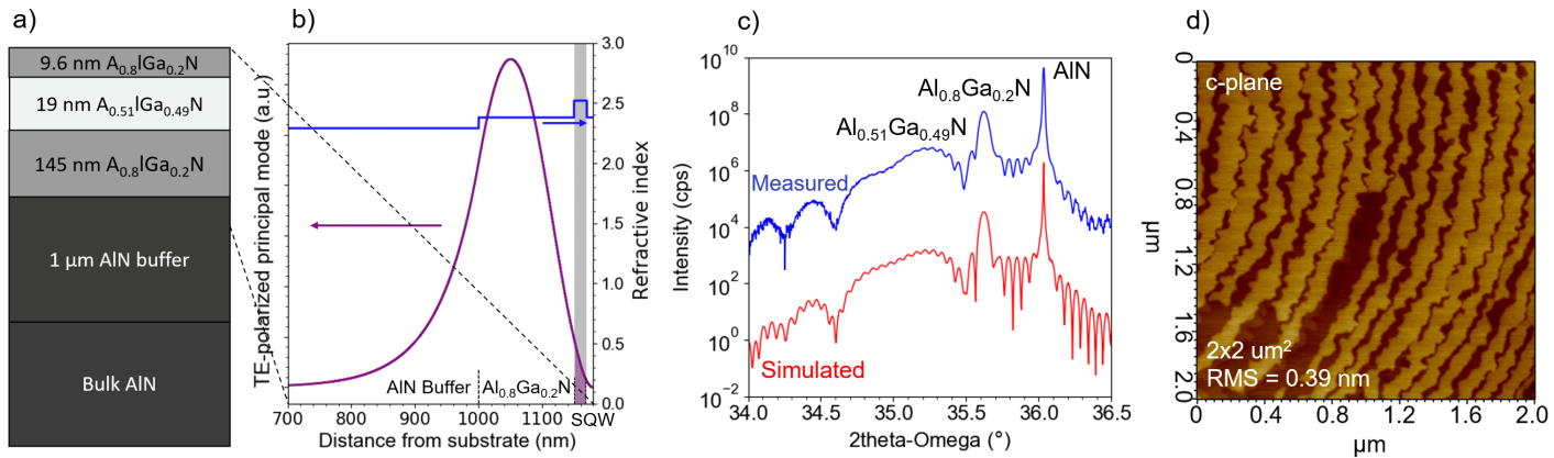
The double heterostructure lasers reported here are grown by PA-MBE on Al-polar, c-plane single crystal AlN substrates with a dislocation density on the order of cm-2. The epistructural layer schematic is shown in Figure 1(a). Prior to introduction to the MBE chamber, the substrates are cleaned with acids to partially remove surface oxides and contaminants, following a procedure reported previously Cho et al. (2020). Immediately before growth, the substrates undergo a second cleaning process consisting of repeated cycles of aluminum deposition and thermal desorption to further remove native oxide layers and enable dislocation-free nucleation. For all samples, a high substrate temperature (TC) AlN buffer layer is grown with a thickness of 1 m to isolate the active region of the device from the remaining impurities present at the substrate interface, which can contribute to optical loss. Following the buffer layer growth, all excess Al is thermally desorbed and the substrate temperature is lowered to C for the growth of the subsequent AlGaN layers. A bottom waveguide is then grown, targeted at a thickness of 150 nm to remove the optical optical field intensity of the principal lasing mode from the AlN-Al0.8Ga0.2N interface, to limit the optical loss from surface-riding impurities formed around that interface Chaudhuri et al. (2021). Then, a 20 nm thick quantum well gain layer is grown aimed at an aluminum composition of 55, followed by a 10 nm Al0.8Ga0.2N cap layer. Excess metal is thermally desorbed from the crystal surface at each heterointerface to ensure sharp interfaces and abrupt compositional change.
The cap layer thickness is chosen to maximize the product of the optical confinement factor, , and the optical gain, . For the quantum well composition of Al0.55Ga0.45N, the lasing optical modes are transverse electric (TE) polarized, meaning that for increasing cap layer thickness, increases as well Zhang et al. (2010). On the other hand, due to generation and recombination of electron-hole pairs in the Al0.8Ga0.2N cap layer upon optical pumping from the surface, the gain of the double heterostructure laser exponentially decreases as a function the cap layer thickness for a given pump intensity. These competing effects are simulated using an optical AlGaN heterostructure solver, SiLENSE. The resulting product is found to be maximized at a cap layer thickness of 10 nm when pumping the double heterostructure from the topside with a 193 nm ArF excimer laser. Such an ArF laser is employed as the source of population inversion for the AlGaN double heterostructure laser reported here. A schematic of the double heterostructure laser, and the accompanying principal TE polarized optical mode and the 2- x-ray diffraction (XRD) scan and simulation around the [0002] wurtzite axis are shown in Figure 1(a)-(c). The simulated XRD plot in Figure 1(c) suggests the thicknesses and composition are close to the target and are given in Figure 1(a). Figure 1(d) shows an atomic force microscopy image of the c-plane surface of the grown double heterostructure laser. Atomic steps due to the miscut angle of the substrate surface are visible. Along with the very low RMS roughness of 0.39 nm, they indicate that the heterostructure was successfully grown in the desired two-dimensional growth mode.
The epistructure in Figure 1(a) was fabricated into both etched facet emitters as well as cleaved facet emitters, as shown in the schematic in Figure 2(a). The sidewalls and facets of the etched facet emitters are formed by inductively coupled reactive-ion etching (ICP-RIE) followed by a tetramethylammonium hydroxide (TMAH) wet etch at 85 ∘C for 10 minutes. The cleaved facet emitters are cleaved after ICP-RIE, followed by a similar TMAH wet etch. The TMAH etch converts the slanted facets and sidewalls resulting from the dry etch or roughened - and -plane surfaces to vertical, smoother walls Yasue et al. (2019). The avoidance of these mirror imperfections is crucial to achieve significant optical feedback from the facets, as described in the next paragraphs.
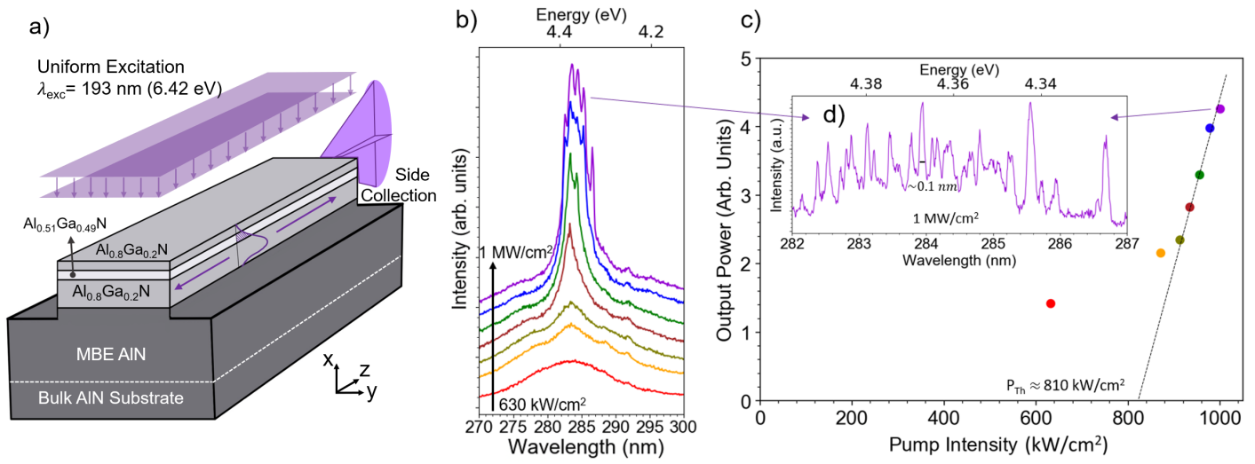
An ArF excimer laser emitting at 193 nm (6.42 eV) is used as the optical pump for the AlGaN laser bars and is pulsed at a width of 10 ns at 2 mJ per pulse with a repetition frequency of 100 Hz. The excitation pattern is focused into a pencil shape by cylindrical lenses for uniform excitation of the top of the DH laser, and the intensity is varied through the use of deep-ultraviolet optical filters. The emission is collected from the facet of the DH laser and its spectrum is measured with a 500 mm focal length spectrometer with diffraction grating of 2400 lines per millimeter with 240 nm blaze wavelength. This is illustrated in the schematic in Figure 2(a).
Figure 2(b) shows the low resolution photoluminescence spectra for a 1 mm long cleaved facet laser for various excitation intensities. As the pump intensity is increased, the spectral FWHM decreases from 15 nm at 630 kW/cm2 to 5 nm at 900 kW/cm2 due to the onset of amplified spontaneous emission. From the output versus input power plot in Figure 2(c), the threshold of light amplification by stimulated emission occurs at 810 kW/cm2. At 1 MW/cm2, this is accompanied with a broad gain spectrum with peak gain at 284 nm and multi-mode emission is realized, as shown in Figure 2(d). The resolution of the spectrometer is limited to 0.01 nm. However, for a laser bar of longitudinal length and effective refractive index , emitting at wavelength , the modal spacing is approximately equal to Sze and Ng (2008). For 1 mm and , 0.013 nm Guo et al. (2020). Since is close to the spectrometer resolution, and some of the modes are suppressed, not all are resolved. The FWHM of the resolved modes is 0.1 nm. It must be noted that a there is a large 2.06 eV of heat generated by phonons due to hot electron-hole pair generation by each absorbed 193 nm ( 6.42 eV) photon. Therefore, the lasing threshold pump intensity can be significantly decreased by increasing the quantum well and cladding layer aluminum compositions (increasing bandgap) or increasing (decreasing) the pump wavelength (energy).
An increasingly important aspect of cavity optics at short wavelength photonic devices is the sensitivity to boundary imperfections, which can be a specially severe bottleneck for deep-UV laser diodes. In order to quantify the importance of laser bar processing optimization, a model for the effect of mirror imperfections on the optical cavity loss of a Fabry-Pérot laser structure is now discussed. To achieve light amplification by stimulated emission, the lasing equation must be satisfied:
| (1) |
where is the confinement factor, the optical gain, the optical intrinsic (material) loss and the optical cavity loss. is the sum of the mirror loss, , and ridge loss, , where the latter is neglected in this discussion. For a Fabry-Pérot cavity with two identical mirrors and length , the mirror loss is given by:
| (2) |
Often, the mirrors are treated as idealized facets defined by a single semiconductor-air interface and reflectance =. However, in practice, the facets often exhibit imperfections such as tilt due to inductively coupled plasma reactive ion etching (ICP-RIE) or cleaving and roughening of the semiconductor-air interface due process inhomogeneities, anisotropic etch rates, or cleaving.
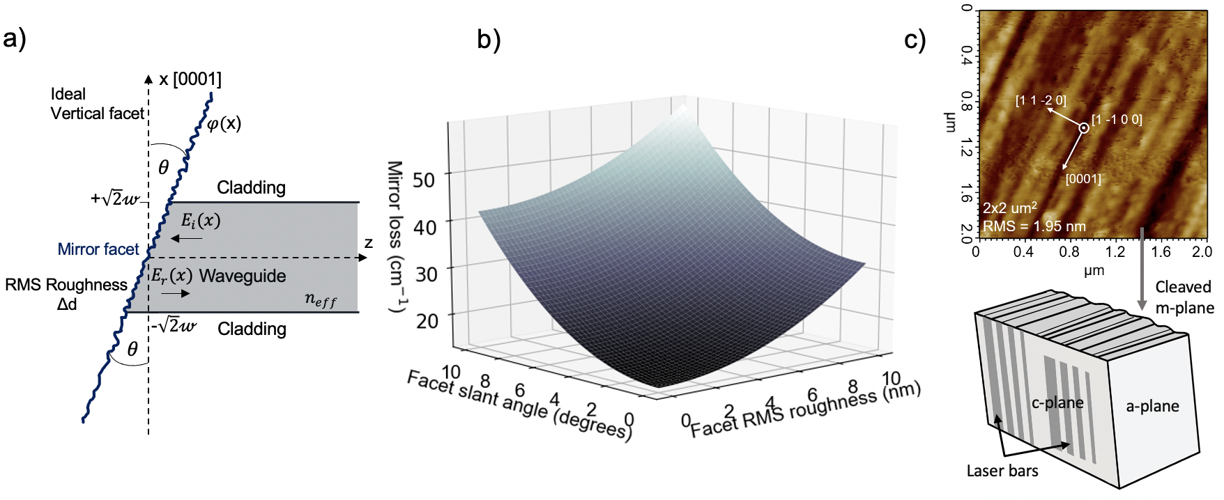
The effects of these imperfections on mirror reflectivity have been discussed seperately by Iga et al. and Stocker et al., respectively Iga et al. (1981); Stocker et al. (1998). Both of the imperfections cause a phase shift of the specularly reflected longitudinal modes of the laser, reducing the net reflectance of the mirrors. The combined effect of facet tilt and roughness is discussed now. This scenario is illustrated in Figure 3(a). First, consider the phase shift due to a facet that is tilted by an angle with respect to the vertical (-axis). At , the TE polarized optical mode, which is the dominant mode for AlGaN quantum wells with a quantum well Aluminum composition below , can be approximated as a Gaussian beam with waist radius at the mirror interface, where is the beam waist Zhang et al. (2010). The incident, transverse principal field at the interface can then be written as:
| (3) |
where the pre-exponential term is the electric field amplitude, and . The phase shift by the longitudinal mode reflected at each point along the mirror is equal to
| (4) |
where is the effective refractive index corresponding to the waveguide and is the free-space wavelength corresponding to the longitudinal lasing mode. Secondly, if the surface of the slanted facet is roughened, following a Gaussian distribution, then the RMS phase broadening can be found by regarding each point along the facet as a Huygens point source:
| (5) |
where is the RMS roughness of the facet surface. Then, the distribution, , of the reflected beam having a phase shift due to the facet roughness, is given by:
| (6) |
Finally, assuming a semiconductor-air reflectivity, , and that the facet roughness occurs at a length scale , we can calculate the net reflectivity, , from the mirror imperfections and incident beam :
| (7) |
where . Using and Equation 2, the final mirror loss of a laser with two identical mirrors with the described imperfections can be written as:
| (8) |
This implies that the mirror imperfection loss scales as the inverse wavelength squared of the longitudinal lasing mode. For example, consider an AlGaN deep-UV cavity with = 250 nm and an InGaN blue cavity with = 450 nm, with / Leung et al. (1998); Muth et al. (1999). The AlGaN cavity exhibits a mirror imperfection loss term 2.5 times as large as an InGaN blue cavity for the same degree of tilt and RMS roughness. For a laser structure similar to the DH discussed here, Figure 3(b) shows a plot of mirror loss as a function of facet slant angle and surface RMS roughness, for = 1 mm, = 280 nm, = 3, and = 50 nm. For example, such a laser bar with and nm corresponds to an approximate doubling of the mirror loss compared to the idealized case. It must be noted that facet slanting between the - and -axis can also occur, which roots a more severe optical mirror imperfection loss since the beam waist is larger in the direction. However, since this slanting is caused by misaligned cleaving, it is easier to avoid. For the processed laser bars, facet RMS roughness as low as 1.95 nm was achieved with near-vertical facets, with an atomic force microscopy image of the facet shown in Figure 3(c). This value corresponds to a theoretical imperfection loss of merely 1.4 cm-1. However, the threshold pump intensity is still fairly high compared to those reported by MOCVD Kirste et al. (2018).
Certain straightforward design and experimental optimizations can be made to reduce the threshold pump intensity. First of all, the active region can be optimized to enhance the gain, such as in a multiple quantum well design Witzigmann et al. (2020). Or, by reducing the difference in Al composition between the quantum well and barriers, the polarization fields are screened at a lower pump intensity. The intrinsic optical loss can be reduced by removing the optical mode from the AlN-AlGaN interface, which can be achieved by increasing the bottom waveguide layer thickness or introducing impurity blocking layers in the AlN homoepitaxial buffer layer Chaudhuri et al. (2021). Further, a large fraction of the pump energy is lost to heat due to the generation of phonons due to hot electron-hole pairs. Hence, pumping the laser bars closer to the band edge should significantly reduce the threshold intensity. Finally, it is noted that the cavity loss for the laser bars discussed here are limited by the single semiconductor-air interface, resulting in the mirror loss of cm-1 for a cavity length of 1 mm, in the ideal case. The threshold pump intensity can be further reduced by reducing this mirror loss. General techniques that are used are high-reflectivity oxides-based distributed Bragg reflectors enabled by atomic layer deposition Sakai et al. (2020), or distributed feedback lasers enabled by electron beam lithography Muziol et al. (2020), but these techniques are mode-selective.
In summary, we achieved multi-mode lasing at 284 nm from side-emitting, optically injected, double heterostructure AlGaN laser structures. This is the first of its kind grown by plasma-assisted molecular beam epitaxy on bulk AlN. The importance of process optimization for Fabry-Pérot lasers emitting at decreasing wavelengths is highlighted by a model for the combined effect of facet slant and roughness on the optical mirror loss. To this purpose, a combination of a dry etch or cleaving followed by a TMAH etch, is utilized, resulting in smooth and vertical facets and mesa sidewalls. Along with electronic design optimization to maximize optical gain, as well as waveguide design and growth optimization to keep the intrinsic optical losses low, the minimization of cavity losses is important in order to achieve room temperature, electrically injected, deep-ultraviolet, continuous-wave laser diodes based on the AlGaN semiconductor materials family.
The data that support the findings of this study are available from the corresponding author upon reasonable request.
The authors thank Professor Farhan Rana, Dr. Shyam Bharadwaj, Dr. Kazuki Nomoto, and Dr. Jimy Encomendero at Cornell University for helpful discussions. This work is partially supported by the Cornell Center for Materials Research with funding from the NSF MRSEC program (No. DMR-1719875). Further support is granted by ULTRA, an Energy Frontier Research Center funded by the U.S. Department of Energy (DOE), Office of Science, Basic Energy Sciences (BES), under Award No. DE-SC0021230. The authors also acknowledge the Cornell NanoScale Facility for device fabrication, supported by the National Science Foundation with grant No. NNCI-1542081 and RAISE-TAQS 1839196, as well as MRI 1631282.
References
- Welch et al. (2018) D. Welch, M. Buonanno, V. Grilj, I. Shuryak, C. Crickmore, A. W. Bigelow, G. Randers-Pehrson, G. W. Johnson, and D. J. Brenner, Scientific Reports 8, 2752 (2018), ISSN 2045-2322.
- Cheng et al. (2020) Y. Cheng, H. Chen, L. A. Sánchez Basurto, V. V. Protasenko, S. Bharadwaj, M. Islam, and C. I. Moraru, Scientific Reports 10, 3411 (2020), ISSN 2045-2322.
- Mezzanotte et al. (2007) V. Mezzanotte, M. Antonelli, S. Citterio, and C. Nurizzo, Water Environment Research 79, 2373 (2007), ISSN 1554-7531.
- Mehnke et al. (2017) F. Mehnke, M. Guttmann, J. Enslin, C. Kuhn, C. Reich, J. Jordan, S. Kapanke, A. Knauer, M. Lapeyrade, U. Zeimer, et al., IEEE Journal of Selected Topics in Quantum Electronics 23, 29 (2017), ISSN 1558-4542, conference Name: IEEE Journal of Selected Topics in Quantum Electronics.
- Allcock et al. (2006) H. R. Allcock, M. V. B. Phelps, E. W. Barrett, M. V. Pishko, and W.-G. Koh, Chemistry of Materials 18, 609 (2006), ISSN 0897-4756, publisher: American Chemical Society.
- Ozawa et al. (2017) A. Ozawa, J. Davila-Rodriguez, J. R. Bounds, H. A. Schuessler, T. W. Hänsch, and T. Udem, Nature Communications 8, 44 (2017), ISSN 2041-1723.
- Taylor and Bowen (2016) M. A. Taylor and W. P. Bowen, Physics Reports 615, 1 (2016), ISSN 0370-1573.
- Park et al. (2018) J. H. Park, D. Y. Kim, E. F. Schubert, J. Cho, and J. K. Kim, ACS Energy Letters 3, 655 (2018), ISSN 2380-8195, 2380-8195.
- Amano et al. (2020) H. Amano, R. Collazo, C. D. Santi, S. Einfeldt, M. Funato, J. Glaab, S. Hagedorn, A. Hirano, H. Hirayama, R. Ishii, et al., Journal of Physics D: Applied Physics 53, 503001 (2020), ISSN 0022-3727, publisher: IOP Publishing.
- Xie et al. (2013) J. Xie, S. Mita, Z. Bryan, W. Guo, L. Hussey, B. Moody, R. Schlesser, R. Kirste, M. Gerhold, R. Collazo, et al., Applied Physics Letters 102, 171102 (2013), ISSN 0003-6951, publisher: American Institute of Physics.
- Zhang et al. (2019) Z. Zhang, M. Kushimoto, T. Sakai, N. Sugiyama, L. J. Schowalter, C. Sasaoka, and H. Amano, Applied Physics Express 12, 124003 (2019), ISSN 1882-0786, publisher: IOP Publishing.
- Sato et al. (2020) K. Sato, S. Yasue, K. Yamada, S. Tanaka, T. Omori, S. Ishizuka, S. Teramura, Y. Ogino, S. Iwayama, H. Miyake, et al., Applied Physics Express 13, 031004 (2020), ISSN 1882-0786, publisher: IOP Publishing.
- Jmerik et al. (2010) V. N. Jmerik, A. M. Mizerov, T. V. Shubina, A. A. Toropov, K. G. Belyaev, A. A. Sitnikova, M. A. Yagovkina, P. S. Kop’ev, E. V. Lutsenko, A. V. Danilchyk, et al., physica status solidi (a) 207, 1313 (2010), ISSN 1862-6319.
- Jmerik et al. (2013) V. N. Jmerik, E. V. Lutsenko, and S. V. Ivanov, physica status solidi (a) 210, 439 (2013), ISSN 1862-6319.
- Hasegawa et al. (2007) H. Hasegawa, Y. Kamimura, K. Edagawa, and I. Yonenaga, Journal of Applied Physics 102, 026103 (2007), ISSN 0021-8979, publisher: American Institute of Physics.
- Jena et al. (2000) D. Jena, A. C. Gossard, and U. K. Mishra, Applied Physics Letters 76, 1707 (2000), ISSN 0003-6951, publisher: American Institute of Physics.
- Cho et al. (2020) Y. Cho, C. S. Chang, K. Lee, M. Gong, K. Nomoto, M. Toita, L. J. Schowalter, D. A. Muller, D. Jena, and H. G. Xing, Applied Physics Letters 116, 172106 (2020), ISSN 0003-6951, publisher: American Institute of Physics.
- Lee et al. (2021) K. Lee, R. Page, V. Protasenko, L. J. Schowalter, M. Toita, H. G. Xing, and D. Jena, Applied Physics Letters 118, 092101 (2021), ISSN 0003-6951, publisher: AIP Publishing LLC AIP Publishing.
- Islam et al. (2017) S. M. Islam, K. Lee, J. Verma, V. Protasenko, S. Rouvimov, S. Bharadwaj, H. (Grace) Xing, and D. Jena, Applied Physics Letters 110, 041108 (2017), ISSN 0003-6951, publisher: American Institute of Physics.
- Bharadwaj et al. (2020) S. Bharadwaj, S. Bharadwaj, J. Miller, K. Lee, J. Lederman, M. Siekacz, H. G. Xing, H. G. Xing, H. G. Xing, D. Jena, et al., Optics Express 28, 4489 (2020), ISSN 1094-4087, publisher: Optical Society of America.
- Lee et al. (2020) K. Lee, S. Bharadwaj, Y.-T. Shao, L. van Deurzen, V. Protasenko, D. A. Muller, H. G. Xing, and D. Jena, Applied Physics Letters 117, 061104 (2020), ISSN 0003-6951, publisher: American Institute of Physics.
- Yasue et al. (2019) S. Yasue, K. Sato, Y. Kawase, J. Ikeda, Y. Sakuragi, S. Iwayama, M. Iwaya, S. Kamiyama, T. Takeuchi, and I. Akasaki, Japanese Journal of Applied Physics 58, SCCC30 (2019), ISSN 1347-4065, publisher: IOP Publishing.
- Chaudhuri et al. (2021) R. Chaudhuri, Z. Chen, D. A. Muller, H. G. Xing, and D. Jena, Journal of Applied Physics 130, 025703 (2021), ISSN 0021-8979, publisher: American Institute of Physics.
- Zhang et al. (2010) J. Zhang, H. Zhao, and N. Tansu, Applied Physics Letters 97, 111105 (2010), ISSN 0003-6951, publisher: American Institute of Physics.
- Sze and Ng (2008) S. M. Sze and K. K. Ng, Physics of Semiconductor Devices (Wiley, 2008), 3rd ed., ISBN 978-0-470-06832-8.
- Guo et al. (2020) Q. Guo, R. Kirste, P. Reddy, W. Mecouch, Y. Guan, S. Mita, S. Washiyama, J. Tweedie, Z. Sitar, and R. Collazo, Japanese Journal of Applied Physics 59, 091001 (2020), ISSN 1347-4065, publisher: IOP Publishing.
- Iga et al. (1981) K. Iga, K. Wakao, and T. Kunikane, Applied Optics 20, 2367 (1981), ISSN 2155-3165, publisher: Optical Society of America.
- Stocker et al. (1998) D. A. Stocker, E. F. Schubert, W. Grieshaber, K. S. Boutros, and J. M. Redwing, Applied Physics Letters 73, 1925 (1998), ISSN 0003-6951, publisher: American Institute of Physics.
- Leung et al. (1998) M. M. Y. Leung, A. B. Djuriŝić, and E. H. Li, Journal of Applied Physics 84, 6312 (1998), ISSN 0021-8979, publisher: American Institute of Physics.
- Muth et al. (1999) J. F. Muth, J. D. Brown, M. a. L. Johnson, Z. Yu, R. M. Kolbas, J. W. Cook, and J. F. Schetzina, Materials Research Society Internet Journal of Nitride Semiconductor Research 4, 502 (1999), ISSN 1092-5783, publisher: Cambridge University Press.
- Kirste et al. (2018) R. Kirste, Q. Guo, J. H. Dycus, A. Franke, S. Mita, B. Sarkar, P. Reddy, J. M. LeBeau, R. Collazo, and Z. Sitar, Applied Physics Express 11, 082101 (2018), ISSN 1882-0786, publisher: IOP Publishing.
- Witzigmann et al. (2020) B. Witzigmann, F. Römer, M. Martens, C. Kuhn, T. Wernicke, and M. Kneissl, AIP Advances 10, 095307 (2020), publisher: American Institute of Physics.
- Sakai et al. (2020) T. Sakai, M. Kushimoto, Z. Zhang, N. Sugiyama, L. J. Schowalter, Y. Honda, C. Sasaoka, and H. Amano, Applied Physics Letters 116, 122101 (2020), ISSN 0003-6951, publisher: American Institute of Physics.
- Muziol et al. (2020) G. Muziol, M. Hajdel, H. Turski, K. Nomoto, M. Siekacz, K. Nowakowski-Szkudlarek, M. Żak, D. Jena, H. G. Xing, P. Perlin, et al., Optics Express 28, 35321 (2020), ISSN 1094-4087, publisher: Optical Society of America.