Noise Scaling in SQUID Arrays
Abstract
We numerically investigate the noise scaling in high- commensurate 1D and 2D SQUID arrays. We show that the voltage noise spectral density in 1D arrays violates the scaling rule of for the number of Josephson junctions in parallel. In contrast, in 2D arrays with 1D arrays in series, the voltage noise spectral density follows more closely the expected scaling behaviour of . Additionally, we reveal how the flux and magnetic field rms noise spectral densities deviate from their expected scaling and discuss their implications for designing low noise magnetometers.
Keywords: noise, SQUID, array, scaling law
\ioptwocol
1 Introduction
Superconducting quantum interference devices, better known as SQUIDs; are used extensively in magnetic sensing applications [1, 2]. When multiple SQUIDs are combined in parallel and in series to form a so-called SQUID array, the response to externally applied magnetic fields can be enhanced and tuned via the number of Josephson junctions and the geometry of the SQUID cells [3–12]. Henceforth, SQUID and superconducting quantum interference filter (SQIF) arrays can be used as highly sensitive magnetometers and low-noise amplifiers in a variety of applications [13–18].
A commonly used characteristic of operation is the voltage-flux response. The SQUID array is current biased and any small applied magnetic flux per loop is converted into voltage across the array. The conversion efficiency is given by the transfer function . The electrical normal resistance of Josephson junctions (JJs) generates Johnson white noise, which causes the appearance of voltage and flux noise in SQUID arrays. Both the transfer function and the noise spectral densities depend on many device parameters. The problem of optimising the common dc SQUID has long been solved [19–21]. In contrast, optimising SQUID arrays is still a partially unsolved problem due to the larger parameter space and computational complexity. The transfer function of 1D and 2D arrays has been studied theoretically [22], but their noise spectral densities have not been simulated yet.
The current paper is organised as follows. In Sec. II we investigate the maximum transfer function of commensurate SQUID arrays with JJs in parallel and JJ rows in series for the case where temperature, critical current, normal resistance and partial inductances are kept constant. In Sec. III we explore the low-frequency voltage noise spectral density and the rms flux and magnetic field noise spectral densities, and their deviation from the expected scaling. Finally, we discuss some of the implications this has for the design of high- SQUID arrays.
2 Array transfer function
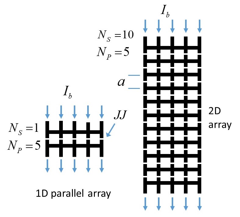
We start by discussing the transfer function of 1D and 2D SQUID arrays, since the transfer function is needed to calculate the flux noise and magnetic field noise spectral densities. We assume that the JJs of the SQUID arrays are over-damped, a valid assumption for YBCO thin film arrays at 77 K, and all arrays have the same normal resistances and critical currents , that is: there is no statistical variation in the junction parameters. The time-averaged voltage, appearing between the top and bottom bias current leads (Fig. 1), is and is normalised by . The transfer function of a SQUID array is , where with the applied flux per SQUID cell and the flux quantum. The transfer function depends on several parameters, which can be grouped into intrinsic, extrinsic and geometric parameters, where
| (1) |
Here, is the only intrinsic parameter as has been absorbed by normalisation. The three external parameters are the applied temperature , the applied total bias current and the flux applied per SQUID cell. The geometrical parameters are the inductance matrix of the commensurate array, the number of JJ rows in series and the number of JJs in parallel in each row. We fix at 77 K which is common for YBCO devices.
To obtain optimal flux-to-voltage transduction, the transfer function of the SQUID array can be maximised by adjusting the external bias current and the external applied flux such that the transfer function is at its maximum. We denote the maximum transfer function at and by .
The theoretical model used here to calculate the maximum transfer functions and the spectral noise densities is simlar to the RSJ simulation model used by Cybart et al. [8]. The mathematical model used here has been discussed in detail in a separate publication [22], which takes into account the effect of thermal noise and mutual inductances.
In the following simulations, we keep and fixed while varying the array geometric parameters and . We use = 20 A, which is a typical value for YBCO step edge JJs [12]. The inductance matrix is defined by the commensurate array layout shown in Fig. 1. Here, the square loop width is = 10 m with track width = 2 m and film thickness 0.2 m. The inductance matrix includes the kinetic inductances where the London penetration depth is taken as m. For the geometric part of the inductance matrix, we use the analytic expressions given in [23]. From the self-inductance of the individual SQUID loops, one finds . The noise strength parameter corresponding to these values and K is , where is the Boltzmann constant. The top and bottom bias leads were taken as 100 m long and their inductances were included in our calculations, though their contributions were found to be negligibly small.
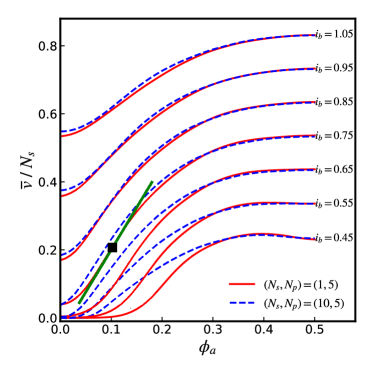
As an example, Fig. 2 shows for the time-averaged voltage , for (red) and (dashed blue), versus the applied flux for different bias currents where is the total bias current (see Fig. 1). We see that depends on . In the case of , the maximum transfer function occurs at and .
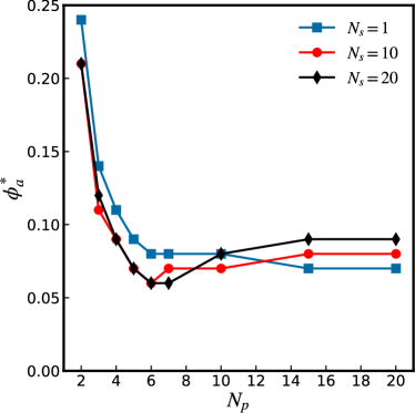
By varying and , we find that occurs at , independent of and . In contrast, the applied flux varies strongly with . As shown in Fig. 3, initially rapidly decreases with increasing . While = 0.25 for the common dc SQUID (), if for both (1D parallel arrays) as well as and 20 (2D arrays).
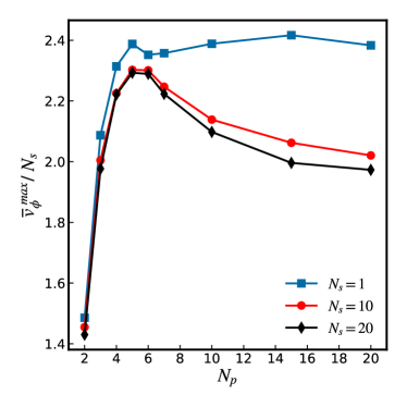
Figure 4 shows versus for (1D parallel arrays) and and 20 (2D arrays). The maximum transfer function initially increases with . However, for , plateaus for the 1D parallel arrays and slightly decreases for the 2D arrays. The levelling of for in Fig. 4 can be understood from calculations performed by Kornev et al. [24, 25] and others [26].
3 Array low-frequency voltage and flux noise spectral density
The voltage noise spectral density can be obtained from the Fourier transform of . The one-sided voltage noise spectral density in dimensionless units (normalised by ) is given by
| (2) |
where is the unit imaginary number. Here, is the time-dependent total voltage between the bias leads of the array, is the spectral frequency in dimensionless units, normalised by , and the time in dimensionless units, normalised by .
The low-frequency voltage-noise spectral density can be calculated from a low frequency analysis as detailed in Tesche & Clarke [19]. This can be done by averaging the total array voltage of the array, i.e.
| (3) |
over time intervals and obtaining a set of averaged voltages [27], where is the voltage corresponding to the th junction (from left to right) in the th row of the array. We then take the Fourier transform of this discrete set and by using Eq. 2 the low-frequency voltage-noise is determined. To enhance the numerical accuracy, we repeat this process up to 7000 times in order to achieve a good ensemble average for . This discrete Fourier transform procedure is accurate subject to the condition [19], where is the normalised fundamental Josephson frequency . In our simulations, we use . In this paper, we limit the size of our arrays to no more than due to the large computation times required to accurately compute .
As the Johnson noise voltages of the JJ’s are uncorrelated and their mean square deviations are identical, one would simplistically expect to obtain the scaling behaviour
| (4) |
This is evident from Eq. 2 and 3: is calculated by taking the arithmetic mean of the junction voltages in parallel, and then summing up the voltage in series for rows.
Similar to , the voltage to voltage-noise ratio SNRv is expected to follow the scaling behaviour
| (5) |
Using our above mentioned 2D SQUID array model, we have calculated the normalised low-frequency voltage-noise spectral density from Eq.2 for 1D parallel arrays and 2D arrays.
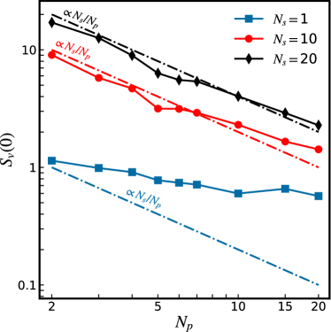
Figure 5 shows versus for (1D parallel arrays) and and 20 (2D arrays) calculated at (Fig. 3) and where the transfer functions have their maxima. The dashed curves indicate the scaling behaviour. The calculation shows that the voltage noise spectral density for the 1D parallel arrays does not follow the scaling but instead, . In contrast, the 2D arrays follow the scaling fairly well.
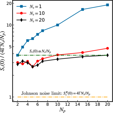
It is also useful to plot relative to the normalised Johnson white noise voltage spectral density for a purely resistive array with resistance . Since the de-normalised white-noise voltage spectral density of a resistor is [28], one finds where is the noise strength. Using the data from Fig. 5, Fig. 6 shows versus for different . Figure 6 clearly reveals the deviations from the scaling, where for perfect scaling the data would follow horizontal lines like the dashed green line. In particular, the 1D parallel arrays (, in red) do not follow the scaling. The orange dashed horizontal line in Fig. 6 is the Johnson noise limit, i.e. , and the 2D SQUID arrays with relatively large get closest to this limit.
Kornev et al. [29, 24] have shown that such a behaviour for in 1D parallel arrays occur due to the emergence of a finite JJ interaction radius [25] but they did not examine the behaviour of 2D arrays.
In practice, the rms flux noise is used as a measure of the device’s performance. It is given by the expression
| (6) |
Since approximately scales with , one expects for the scaling behaviour
| (7) |
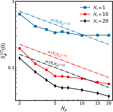
Figure 7 shows the calculated low-frequency rms flux noise versus for different . The were obtained from Eq. 6 at and . As can be seen, for the three different the deviations from the scaling (dashed straight lines) are similar. This is due to the factor in Eq. 6.
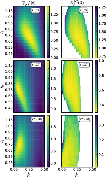
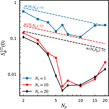
A revealing measure for the rms flux noise of a SQUID array is the dimensionless quantity defined as
| (9) |
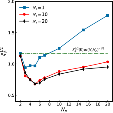
The result for Eq. 9, evaluated at and , is displayed in Fig. 8 showing versus for different . Compared to Fig. 7, Fig. 8 reveals the relative deviation from the scaling. In the case of perfect scaling, the data would lie on horizontal straight lines similar to the green dashed line.
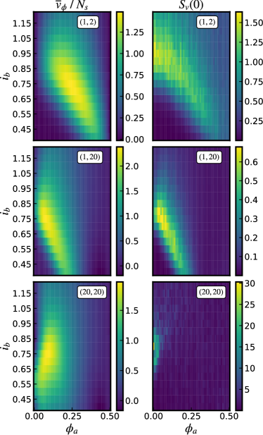
It is important to note that the values which maximise do not minimise the voltage noise . Figure 9 shows the distribution of and values for a range of and , not just and . Similarly, one can plot for multiple and see how it compares to . Figure 10 shows several heatmaps for differently-sized arrays. They show that is approximately minimised in the neighbourhood where is a maximum for the (1,2) and (1,20)-arrays. However, this is not the case for the (20,20)-array, which indicates that one cannot optimise both the transfer function and noise of the array with the same values for arrays of arbitrary size.
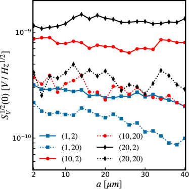
We now proceed to de-normalise the normalised voltage noise spectral density . This is done by multiplying by . Using [1], we compute the rms voltage spectral density for different SQUID cell sizes and show the results in Fig. 11.
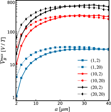
In a similar manner, one can de-normalise the normalised transfer function to obtain . This is achieved by multiplying by where is the effective area of the SQUID cell, which in our case is . The results for as a function of are shown in Fig. 12.
The normalised rms flux noise is de-normalised by multiplying with . Using again the junction parameters at K of and A one obtains . Using the normalised value from Fig. 10 corresponding to the array, one finds an rms flux noise of . In contrast, the rms flux noise of the -array is 10 times higher, while according to the scaling behaviour in Eq. (8) it should be times higher.
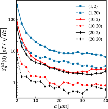
The rms magnetic field noise spectral density is obtained by dividing the rms flux noise by the SQUID loop area , or simply by calculating . This gives for the array with a value of . This result is consistent with the literature, for instance Couëdo et al. [30] reported a white noise measurement of fT on a (300,2)-SQIF array made of YBCO and operating at K. By contrast, in low-temperature dc-SQUIDs operating at K, one often finds using pick-up coils (see for instance Drung et al. [31, 32]). Similarly, earlier work on high- YBCO dc-SQUIDs operating at 77 K showed that by coupling the SQUID to a large pickup loop of millimetre size, that could be reduced down to fT [33].
In the case of SQUID arrays, can be reduced further by increasing . For instance, Fig. 13 shows as a function of , and we see that increasing both and contributes to a reduction in noise. Furthermore, since is relatively flat with as shown in Fig. 11, and increases with but plateaus beyond m, in Fig. 13 stops decreasing for larger . The lowest noise level achieved in Fig. 13 is for a (20,20)-array with loop-size m, which represents a two-fold improvement from the array with loop-size m.
It should be noted that variations in the parameters can change the simulation results. From Figures 12 and 13, one sees an increase in the maximum transfer function with increasing for constant , which in turn leads to a decrease in the magnetic field density noise . If one instead keeps the loop area constant, but varies the of the JJs; one obtains different results from the ones presented in this paper. For instance, choosing a lower decreases but increases the magnetic field density noise , while a higher increases but lowers . This is consistent with the fact that since and , one expects the noise level to decrease as grows larger. This implies one can further improve the device’s robustness to noise by increasing the critical current of the junctions.
Lastly, we must discuss the case in which are selected to minimize instead of maximizing . Fig. 14 shows the minimized as a function of and , which exhibits a significantly different trend to Fig. 7: the rms flux noise has a clear minimum near which becomes more prominent for larger . At and , which is over 10 times smaller than in Fig. 7. However, this comes at the cost of a smaller transfer function: in this case, compared to the optimum in Fig. 4. This shows that the choice of can either maximise or minimise , but not both simultaneously.
4 Conclusion
In this paper, we have shown through numerical simulations how the noise scales in 1D and 2D SQUID arrays with respect to the number of junctions. In 1D SQUID arrays we observed a voltage noise spectral density scaling. In contrast, the voltage noise spectral density of 2D arrays follows the scaling closely. Though increasing beyond a certain value will not further increase the maximum transfer function, it further reduces the voltage noise spectral density. The rms flux noise, which is inversely proportional to the transfer function; deviates from the expected scaling for both the 1D parallel arrays and the 2D arrays when is optimised. Furthermore, we have shown that one cannot optimise the transfer function as well as the flux noise of the array using the same bias current and flux values unless . By varying the cell size for a given array , one can further reduce the magnetic field noise spectral density without compromising the maximum transfer function. This indicates that there is still room for exploration in the improvement of high- SQUID arrays for sensing applications.
References
References
- [1] Clarke, J. and Brakinski, A. 2006 Wiley-VCH, Weinheim.
- [2] Fagaly, R. L. 2006 Rev. Sci. Instruments 77 101101.
- [3] Miller, J. H. and Gunaratne, G. H. and Huang, J. and Golding, T. D. 1991 Appl. Phys. Lett. 59 3330.
- [4] Oppenländer, J. and Häussler, Ch and Schopohl, N. 2000 Phys. Rev. B 63 024511.
- [5] Müller, K–H. and Mitchell, E. E. 2021 Phys. Rev. B 103 054509.
- [6] Müller, K–H. and Mitchell, E. E. 2024 Phys. Rev. B 109 054507.
- [7] Longhini, P. and Berggren, S. and Palacios, A. and In, V. and de Escobar, A. L. 2011 IEEE TRans. Appl. Supercond. 21 391.
- [8] Cybart, S. A. and Dalichaouch, T. N. and Wu, S. M. and Anton, S. M. and Drisko, J. A. and Parker, J. M. and Harteneck, B. D. and Dynes, R. C. 2012 J. Appl. Phys. 112 063911.
- [9] Dalichaouch, T. N. and Cybart, S. A. and Dynes, R. C. 2014 Supercond. Sci. Technol. 27 065006.
- [10] Taylor, B. J. and Berggren, S. A. E. and O’Brian, M. C. and deAndrade, M. C. and Higa, B. A. and Leese de Escobar, A. M. 2016 Supercond. Sci. Technol. 29 084003.
- [11] Cho, E. Y. and Zhou, Y. W. and Khapaev, M. M. and Cybart, S. A. 2019 IEEE Trans. Appl. Supercond. 29 1601304.
- [12] Mitchell, E. E. and Müller, K–H. and Purches, W. E. and Keenan, S. T. and Lewis, C. J. and Foley, C. P. 2019 Supercond. Sci. Technol. 32 124002.
- [13] Ramos, J. and Zakosarenko, V. and Ijsselsteijn, R. and Stolz, R. and Schultze, V. and Chwala, A. and Hoenig, H. E. and Meyer, H. G. 1999 Supercond. Sci. Technol. 12 597.
- [14] Bruno, A. C. and Espy, M. A. 2004 Supercond. Sci. Technol. 17 908.
- [15] Kornev, V. K. and Soloviev, I. I. and Klenov, N. V. and Mukhanov, O. A. 2010 IEEE Trans. Appl. Supercond. 21 394–398.
- [16] Zhou, X. and Schmitt, V. and Bertet, P. and Vion, D. and Wustmann, W. and Shumeiko, V. and Esteve, D. 2014 Phys. Rev. B 89 214517.
- [17] Chesca, B. and John, D. and Mellor, C. J. 2015 Appl. Phys. Lett. 107 16.
- [18] Chesca, B. and John, D. and Cantor, R. 2021 Appl. Phys. Lett. 118 4.
- [19] Tesche, C. D. and Clarke, J. 1977 J. Low Temp. Phys. 29 301.
- [20] Bruines., J. J. P. and de Waal, V. J. and Mooij, J. E. 1982 J. Low Temp. Phys. 46 383.
- [21] Kleiner, R. and Koelle, D. and Ludwig, F. and Clarke, J. 2004 Proceedings of the IEEE 92 10 1534–1548.
- [22] Galí Labarias, M. A. and Müller, K–H. and Mitchell, E. E. 2022 Phys. Rev. Appl. 17 064009.
- [23] Hoer, C. and Love, C. 1965 J. Res. Nat. Bureau Standards C. Eng. Instrum. 69 127.
- [24] Kornev, V. K. and Soloviev, I. I. and Klenov, N. V. and Filippov, T. V. and Engseth, H. and Mukhanov, O. A. 2009 IEEE Trans. Appl. Supercond. 19 916.
- [25] Kornev, V. K. and Soloviev, I. I. and Klenov, N. V. and Mukhanov, O. A. 2011 IEEE Trans. Appl. Supercond. 21 394.
- [26] Galí Labarias, M. A. and Müller, K–H. and Mitchell, E. E. 2022 IEEE Trans. Appl. Supercond. 32 1600205.
- [27] Enpuku, K. and Muta, T. and Yoshida, K. and Irie, F. 1985 J. Appl. Phys. 5 1916.
- [28] Nysquist, H. 1928 Phys. Rev. 32 110.
- [29] Kornev, V. K. and Arzumanov, A. V. 1997 Inst. Phys. Conf. Ser., IOP Publishing Ltd. 158 627.
- [30] Couëdo, F. and Recoba Pawlowski, E. and Kermorvant, J. and Trastoy, J. and Crété, D. and Lemaître, Y. and Marcilhac, B. and Ulysse, C. and Feuillet-Palma, C. and Bergeal, N. 2019 Appl. Phys. Lett. 114 19.
- [31] Drung, D. 1991 Supercond. Sci. Technol. 4 377.
- [32] Drung, D., Abmann, C., Beyer, J., Kirste, A., Peters, M., Ruede, F. and Schurig, T. 2007 IEEE Trans. Appl. Supercond. 17 699–704.
- [33] Koelle, D. and Kleiner, R. and Ludwig, F. and Dantsker, E. and Clarke, J. 1999 Rev. Mod. Phys. 71 631.