Monarch: A Durable Polymorphic Memory For Data Intensive Applications
Abstract
3D die stacking has often been proposed to build large-scale DRAM-based caches. Unfortunately, the power and performance overheads of DRAM limit the efficiency of high-bandwidth memories. Also, DRAM is facing serious scalability challenges that make alternative technologies more appealing. This paper examines Monarch, a resistive 3D stacked memory based on a novel reconfigurable crosspoint array called XAM. The XAM array is capable of switching between random access and content-addressable modes, which enables Monarch (i) to better utilize the in-package bandwidth and (ii) to satisfy both the random access memory and associative search requirements of various applications. Moreover, the Monarch controller ensures a given target lifetime for the resistive stack. Our simulation results on a set of parallel memory-intensive applications indicate that Monarch outperforms an ideal DRAM caching by on average. For in-memory hash table and string matching workloads, Monarch improves performance up to over the conventional high bandwidth memories.
Index Terms:
Reconfigurable Memory, Data-Intensive, Content Addressable Memory, Data Parallel, Novel Memory Systems1 Introduction
With data being generated at such unfathomable pace and quantity, large memories and cache architectures have become the need for big data processing. While on-chip memories are fast, they are limited in size due to power and area consumption. On the other hand, off-chip memories, albeit being large, suffer from low bandwidth and costly off-chip data movement. Off-chip memories also suffer from the so called bandwidth wall due to the pin count limitations Instead, the through-silicon via (TSV) technology has enabled 3D die-stacked memories that can offer a high bandwidth in excess of terabytes per second [1]. The primary target of such high bandwidth memory has been in-package DRAM for caching and near-data processing.
In-package DRAM faces significant challenges for large-scale data-intensive computing. The latency of accesses to 3D die-stacked DRAM is almost identical to that of the conventional off-chip DRAM. Therefore, DRAM-based in-package caching becomes complex, costly, and often inefficient [2, 3]. Furthermore, an in-package DRAM consumes significant power due to periodic refreshing, large row activation, and multi-level row buffering throughout the memory chips. In addition to consuming a significant portion of the system energy, the DRAM power may lead to serious thermal issues in the 3D memories. In particular, this low energy-efficiency results in concerns for the future of DRAM as the need for low-power high-efficiency data processing is never ending. Moreover, the performance gap between main memory and conventional data storage has been increasing, which is leading to the rise of in-memory database (iMDB) storage for minimizing the query response time [4].
Prior work such as Jenga [5] have looked at defining application-specific cache hierarchies than rigid ones, which eliminates inefficiencies caused by conflicting needs of different applications. Recent work on profiling google consumer workload [6] shows that data movement contributes to a significant portion of total energy consumption. The majority of this data movement comes from simple primitives across multiple applications, which are good candidates for processing-in-memory. This provides good motivation for developing a low-cost reconfigurable memory that allows the software to allocate its resources for caching or in-memory processing.
Researchers have been actively looking into alternative technologies for main memory. Non-volatile memories like resistive RAM (RRAM) and phase-change memory (PCM) exhibit promising results for the future memory systems. There have been numerous recent proposals examining 3D stacks with resistive memories. In particular, RRAM has shown extra capabilities for in-situ operations beyond caching and storage, ranging from combinatorial optimization to machine learning and DNA sequence alignment [7, 8]. This makes it interesting to explore enabling in-situ application specific computing as part of the 3D die-stacked memory.
The main contributions of the paper are as follows. (1) Monarch provides the semantics of interfacing commands for a high-bandwidth resistive memory. We provide the primitives for exploiting cache and search capabilities in high bandwidth resistive memories. (2) The paper provides a comprehensive design for a novel array structure using 2R cells that supports efficient reconfiguration between CAM and RAM. We also examine novel architectural mechanisms for column and row writes in XAM arrays through diagonal organization. (3) A novel architectural mechanism for toggle-based vault control is proposed that vastly minimizes the controller complexity while ensuring efficient and highly parallel data movement. (4) This paper identifies the issues with write endurance and proposes techniques for ensuring a lower bound of lifetime.
2 Motivation and Challenges
Classically, computer systems employ two or three levels of SRAM caches to extract maximal latency and bandwidth benefits of data access. SRAM caches are usually multi-way set associative with addressable sets containing multiple cache-lines, each one distinguishable by a tag. The complexity of tag management may be afforded for the SRAM caches due to their low set-associativity and capacity. However, in 3D die-stacked DRAM caches, tag management remains a significant challenge. Although there has been research on alleviating this issue [9, 10] DRAM caches suffer the absence of a structure that supports high set-associativity at low latencies.
Content addressable memory (CAM) offers a natural solution for tag comparison in large set-associative caches. However, incorporating CAM in the conventional 3D die-stacked DRAM is a major challenge. Unlike DRAM, RRAM has been shown capable of large-scale in-situ parallel bitwise XOR/XNOR [11], which makes it an ideal choice for large-scale CAM designs. Prior work has made such CAM structure visible to the cache controller only [11]. Interestingly, the inherent nature of CAM structures make them suitable for indexing applications requiring large-scale parallel searching, such as hash tables and string matching. Large scale parallel index-based searching is a very prevalent application in database systems [12].
Exploitation of such CAM like structures for in-situ computing requires changes in the peripheral circuitry and user-space control. Fortunately, in RRAM based memories, the control mechanism is relaxed in comparison to the DRAM counterparts, given that RRAM-based memories have no need to issue refresh (R), precharge (P), and activate (A) commands. This makes it worth exploring the possibility of replacing these commands with the ones specifically used for software control over memory for in-situ computing. In particular, we can design an API that communicates with the memory controller to perform application specific in-situ computation by repurposing the existing interface commands. Notably, the use of CAM or RAM depends on the nature of user applications, hence a general solution with static allocation of RAM vs CAM is sub-optimal for the general case. This paper explores reconfigurability of RRAM such that the same XAM array may be used in either CAM or RAM mode.
Design Challenges
Last-level caches with 3D die-stacked memories incur significant write-bandwidth due to write backs from on-chip L3 and cache-line installation on cache-miss. Non-volatile memories like RRAM usually have a limited write endurance, due to which some cells die after a specific number of writes to them (usually [13]) This poses a significant challenge for employing RRAM-based caches, even more so because 3D stacked memories have a higher bandwidth than the conventional off-chip memory. This also poses security challenges where-in a malicious application can exploit frequent writes to the same block and render the memory unusable. Monarch employs multiple techniques and solutions to keep lifetime at an acceptable level. (1) Monarch introduces a new timing parameter, , which imposes a timing constraint between successive writes to the same region of memory. This timing parameter cannot be enforced at fine granularity; therefore, Monarch introduces a set technique for viable implementation of the timing parameter.
(2) On top of the proposed timing constraint, Monarch employs a rotary technique at the same granularity to further enhance the lifetime, while maintaining a superior performance compared to an idealistic DRAM cache system. (3) Monarch adopts optional write-through directly to the off-chip main memory, along with access no-allocate, thereby eliminating unnecessary writes to Monarch.
3 Overview
Figure 1 shows the overview of an example in-package Monarch. Similar to the existing proposals for die-stacked DRAM [1], a stack of 4-8 Monarch layers is connected to the processor die using a high bandwidth interface The Monarch layers are divided into multiple independent vaults, each of which has a separate controller. Monarch is capable of switching the functionality of each bank between random accessing (RAM) and content addressing (CAM) modes. This novel capability enables the high-level software to choose between a hardware-managed cache policy and a scratchpad memory management for each Monarch vault. Monarch follows a similar approach to the one in Intel’s Knights Landing [14] for setting the operational mode and size of the RAM and CAM parts within each vault.
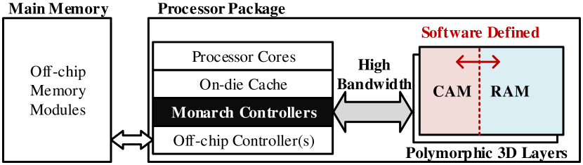
When a vault is configured for hardware-managed caching, the vault controller becomes responsible for automatic cache operations such as tag check, block installation, eviction, and replacement. Therefore, a portion of the vault is turned into CAM for hardware-managed tag storage; while, the rest is used for storing cache data in the RAM mode. The addressing space and operations of each hardware-managed vault remain invisible to the high-level software applications. In contrast, a software-managed vault is visible to the user application through a specific address space for scratchpad operations. Monarch extends this flexibility by allowing the scratchpad memory to be used in the RAM, CAM, or a mix of both modes.
4 XAM: Reconfigurable RAM/CAM
The design of XAM (Figure 2) is based on the 2R cell structure proposed by the prior work, which enhances the read margin and alleviates the sensing error due to sneak currents and leakage in resistive crossbars. Additionally, XAM supports both column and row writes. The differential bit representation makes it capable of performing bit-wise XNOR, thereby parallel searching within the array. Here, we explain the proposed operations for XAM.


4.1 XAM Write
As shown in Figures 3, writing data to XAM relies on the basics of programming bipolar memristive cells [15]. To make the figures easy to follow, every memristive element is shown with a black strip on one terminal. Entering a write current from the black terminal sets the resistive state to low; otherwise, the cell is programmed to a high resistive state. Similar to the prior work [4], XAM follows a two-step write process for writing 0s and 1s. However, special considerations are necessary to enable row- and column-wise wirtes.
4.1.1 Writing a XAM Row
For writing a row, a multi-bit input is inverted and fed in through the column drivers at the top edge (Figures 3 (a) and (b)). All the vertical line corresponding to input 0s are connected to , while the remaining vertical lines (representing 1s) are set to ground (). Only one row is active and all the other rows are kept inactive by connecting them ro . To write a 0, the horizontal lines of the active row are first connected to ground (), which creates a potential drop and a current flow as shown in Figure 3(a). This current flow corresponds to writing a 0 into the selected XAM cells whose vertical line is connected to . All the other cells of the array remain unchanged. The second step begins by switching the voltage level of active horizontal lines from to , which results in stopping the flow of current for writing 0s. Instead, new currents for writing 1s start to flow (Figure 3(b)).
4.1.2 Writing a XAM Column
The data to be written is fed in through the row driver onto the horizontal lines (Figures 3(c) and (d)). Similarly, 0s are written first followed by 1s. Initially, both horizontal lines of each row are connected to either or with respect to the bit value being stored in the row. One column is activated while the rest are kept inactive by setting their vertical lines to . First, the active column is connected to for writing any input 0s. Notably, writing a 0 row-wise and column-wise produce the same cell state. Second, a voltage switch from to is necessary to stop writing 0s and to begin storing 1s (Figure 3(d)).
4.2 XAM Read and Search
Configuring a XAM array for reading or searching requires (1) a XAM datapath that supports communicating address/data bits and (2) a proper reference for sensing bit values.
4.2.1 Reading a XAM Row
Figure 3(e) shows the process of reading a XAM row. First, the row is activated for reading by connecting its and to a read voltage () and ground, respectively. As a result, each XAM cell becomes a voltage divider between its horizontal lines to develop a potential on its vertical line. The amount of this voltage is determined by . Intuitively, a 0 () corresponds to a near potential and a 1 () develops a near voltage. A sensing circuit is employed to compare this potential against a read reference () for producing a bit of the output. We set to for reads.
4.2.2 Searching among XAM Columns
A XAM search can be viewed as an extended read operation, where the horizontal lines are activated based on the contents of an input key and the sensing reference is recomputed to differentiate between a column match and mismatch (Figure 3(f)). First, the input key is applied to the horizontal line drivers. A 0 results in connecting and respectively to and ; while, a 1 creates the opposite line voltages. This complementary application of the key bits to the horizontal lines results in two possibilities for each cell: (1) the low resistive element of the cell is connected to ground that corresponds to a bit mismatch; and (2) the low resistive element is connected to that reads to a bit match. Then, the sensing circuits convert the line voltages to binary values. If all the cells within a column are match, the vertical line voltage remains near ; therefore, the sensing circuit produces a 1 at the output, which indicates a column match. Otherwise, each bit mismatch pulls down its line voltage such that even a single bit mismatch can drop the voltage below . Therefore, the column will be represented by a 0 at the sensor’s output. For a XAM array with rows, should be set to a voltage between all match () and single mismatch (); where, and correspond to the high and low resistances of the memristive elements.
5 Choice of Technology for RAM/CAM
This section compares the latency, energy, and area overheads of a 32KB reconfigurable RAM/CAM block using the CMOS, DRAM, and RRAM technologies (Table I).
Latency
The CMOS unit for SRAM+SCAM has the best read latency, followed by 1R and XAM. SRAM has a and better write latency than DRAM and RRAM. The search latency of SRAM, DRAM, and 1R are much higher than the others due to the fact that they support serial search rather than parallel. Instead, SCAM provides the shortest lookup time, followed by XAM and 2T2R.
Energy
SRAM and SRAM+SCAM exhibit the best read energy, followed by 1R and XAM. The search energy of XAM and 2T2R are low due to their efficient in-situ XNOR operations. SCAM requires a low write energy but a significant search energy due to its cell complexity. An RRAM write require magnitudes higher energy than SRAM and DRAM.
Area
The 1R array consumes the least area, which is similar to that of XAM. The area of a XAM array is about smaller than the SRAM+SCAM.
| Latency (ns) | Energy (nJ) | ||||||
|---|---|---|---|---|---|---|---|
| Read | Write | Search | Read | Write | Search | Area (mm2) | |
| SRAM | 0.2334 | 0.1892 | 14.9395 | 0.015 | 0.0196 | 0.9627 | 0.0331 |
| SCAM | 32.2385 | 0.2167 | 0.5037 | 0.2329 | 0.0139 | 0.1273 | 0.111 |
| SRAM+SCAM | 0.2334 | 0.2167 | 0.5037 | 0.015 | 0.0335 | 0.1273 | 0.144 |
| DRAM | 2.5945 | 2.1874 | 166.0499 | 0.0657 | 0.058 | 4.4544 | 0.0169 |
| 1R RAM | 1.654 | 20.258 | 105.856 | 0.0214 | 0.325 | 1.623 | 0.0104 |
| 2T2R CAM | 122.048 | 20.825 | 3.36 | 2.7156 | 1.29 | 0.0472 | 0.0153 |
| 1R+2T2R | 1.654 | 20.825 | 3.36 | 0.0214 | 1.61 | 0.0472 | 0.0258 |
| 2R XAM | 1.7734 | 20.323 | 3.2264 | 0.0215 | 0.652 | 0.0263 | 0.0124 |
Overall, 1R, SRAM+SCAM, and XAM could give configurations optimized for the specific metrics mentioned above. DRAM is a default baseline considering its widespread use in the existing off-chip and on-chip memories. Therefore, we select three technologies to build the 3D baseline system: 1R RRAM, CMOS SRAM+SCAM, and DRAM. Note that XAM process is CMOS compatible, thereby manufacturable on the processor die. But its capacity would be very less to capture the complete behavior of big data applications. On the other hand, off-chip integration of Monarch would encounter a limited bandwidth making it a poor choice for caching. Therefore, we consider Monarch as an in-package high-bandwidth memory flexibly used for cache, associate search, and scratchpad memory.
Stack Model
Considering a 4GB DRAM stack with 8 layers divided into 8 vaults, a total of 64 segments each sized 64MB are necessary. We consider the same configuration for all the baselines using segments that consume the same area across all the technologies. This provides an iso-area comparison among the systems, with memory capacities of 8GB (1R RRAM), 8GB (Monarch), and 73MB (CMOS).
6 Monarch Organization
Monarch follows the HBM2 3D organization proposed by the prior work on Fine-Grained DRAM [18]. However, a novel datapath is used to support RAM and CAM arbitration. XAM enables such flexibility at low cost by leveraging a toggle-based mechanism to set the operational mode of each bank.
6.1 Monarch Physical Layout
Within each Monarch bank, XAM arrays are physically grouped into supersets that share the same H-trees for data and address. Each superset consists of data/mask/key buffers, a port selector, and multiple XAM arrays (Figure 4).

Diagonal Set Arrangement
A key challenge for designing supersets is the increasing complexity of interconnects for supporting CAM and RAM operations. We alleviate this complexity through (1) sharing the address and data interconnects at the bank and vault levels and (2) accessing the superset arrays diagonally. As shown in Figure 4, sets are organized diagonally in an superset: each subarray at row and column belongs to set (). For every access, only 8 subarrays of a set are selected. The port selector’s job is to enable the path for sending inputs to the right port of the subarrays. Figure 4(a) shows how the column ports for set 0 are selected; whereas, row ports are enabled in Figure 4(b). As the diagonal layout of the sets is fixed, the port selector only requires a latch for holding a mode flag and a 3-to-8 decoder for selecting the corresponding XAM arrays.
6.2 Monarch Interface
Monarch is based on the proposed resistive XAM technology that provides a slower write speed and a comparable read speed to DRAM. One effective technique to reduce the write latency in RRAM is multi-banking that has been frequently suggested by prior work.Following the same logic, Monarch employs a high bandwidth interface that allows the processor to access a large number of parallel banks across multiple vaults. The Monarch interface is designed after the JEDEC high-bandwidth DRAM [19]. DRAM necessitates a set of parameters and commands—i.e., refresh, precharge, activate, read, and write—to be included in the standard. As the DRAM command are not sufficient for XAM operations, we redefine the semantics of parameters as listed in Table II. Therefore, we map the existing commands to XAM-semantics and derive XAM-specific values for the timing parameters. Figure 5 illustrates a summary of key timing parameters proposed for the Monarch interfacing protocol.

Description bank preparation time including setup delay for superset activation time (mainly datapath activation delay) same as the time to complete a read or search (depending on the bank mode) and transferring sensing results to the vault interface the time for sending address and command bit to the TSV stripe read cycle time (max of the interconnects delay and sensing) the time to complete the proposed 2-step data write write cycle time (max of the interconnect delay and ) the time to transfer data from the TSV stripe to a set same as the time to burst data in the TSVs and silicon interposer the time window for M writes
Preparing a Bank
Monarch introduces a prepare command (P) as a replacement for the DRAM precharge. During a bank prepare, the Monarch controller toggles the mode of a bank between CAM and RAM. The initial mode of all Monarch banks is set to RAM. In DRAM, a precharge is necessary in the case of a row conflict—i.e., the row buffer contains a different row than the one is to be accessed. DRAM row conflicts may happen frequently during the execution of a program. Whereas, a bank prepare is only necessary if the controller decides to change the read mode of all the XAM arrays inside the bank. Upon receiving a prepare command, the bank controller makes an internal state transition by switching the sensing reference between and using bank-level voltage level converters [20]. Moreover, the supersets inside the bank will be configured for upcoming search () or read () operations. The default read mode of each bank is read, which makes it possible for the Monarch controller to track the mode of all banks.
Activating a Superset
Instead of a DRAM row activation, Monarch may issue an activate command (A) to a superset before bursting data on the interface. The main purpose of the new activate command is to change the internal datapath of a superset prior to writing data in the RowIn and ColumnIn modes. The DRAM activates, however, are necessary for accessing the missing rows in the row buffer. To keep the controller simple, issuing an activate command toggles the operational mode of the port selector between the column and row access. A bit flag for each superset is adequate to track the state of all supersets at the Monarch controller.
Fine-grained XAM Access
In addition to data buffer, each superset employs a mask and a key buffer for accessing the selected set in the CAM mode. Prior to a search, the keys and bit-masks are sent from the Monarch controller to the superset. We use write command for key/mask transfer. To distinguish between a CAM write and a key/mask write, the superset does not allow writing an input block to the XAM arrays if the mode is set to RowIn for CAM. Instead, a block in the RowIn mode is only written to the mask or key registers if the row address is odd or even, respectively. This enables searching keys with different lengths and arbitrary alignments within arrays. The mask register is also used for partial updates to the data in the ColumnIn mode. This capability is useful for updating the dirty bits of cache tags in one access (Section 7).
Constraining Block Writes
To ensure a lower bound lifetime for Monarch, we introduce a new timing parameter () that limits the number of writes per block within a time window. Given a write endurance () for the XAM cells, the minimum lifetime () is computed by , where is the time window during which a single write per block is allowed. To allow writes per window while guaranteeing the same lifetime, a wider time window is necessary, which is computed by . For example, to ensure a 3-year lifetime ( seconds) with a cell endurance of writes, has to be seconds. Indeed, naively enforcing such timing constraint is impractical due to high complexity and performance overheads. Section 8 explains how Monarch implements .
7 Monarch Control
Monarch supports three modes: flat-RAM, flat-CAM, and cache. The flat modes are managed by software through their visible address spaces at the application level. However, the cache mode is completely hardware-managed at the Monarch controller. For example, an eight-vault Monarch may be configured to 2 flat-CAM, 2 flat-RAM, and 4 cache vaults.
Flat-RAM Control
A flat-RAM vault is supposed to service only two types of requests (i.e., read and write) generated by software. Multiple counters are used to track the required delays between pairs of commands before sending each command to the Monarch layers. Moreover, the controller needs to ensure that the target bank/superset is set to RowIn RAM.
Flat-CAM Control
Extra components are necessary to enable the flat-CAM mode. First, the controller needs to recognize four different types of software generated requests: data write, search, key/mask write, and data read. Second, the controller may require transitioning the target Monarch bank/superset to different modes prior to serving a request. A data write may be carried out only if the target bank/superset is in the ColumnIn CAM mode. The software is expected to populate the XAM arrays using data writes prior to a search. Figure 6 shows an illustrative example code for operation of CAM through a simple key-value store. The key and data values are initially written into the CAM and RAM scratchpads (a single set each in this example), which is followed by updating the key/mask registers, searching the set, and accessing data based on the value returned by the match pointer.

Four pointers are employed for accessing the elements of data, key, mask, and match. For simplicity, assume that the data is a 2D array of a 64-bit type. Each block of 8 data elements is stored across 8 subarrays. A total of 64 blocks are written in a single set. flat_RAM_malloc and flat_CAM_malloc are the proposed function calls for allocating memory within the RAM and CAM scratchpad regions respectively, explained in detail later in this section. Next, the key/mask values are updated through 8 normal writes in the code. However, any accesses to the key/mask pointers are recognized by the flat-CAM controller for special service. First, the key/mask pointers are mapped onto two global registers in the vault controller, which are used for any upcoming search operations. Second, the contents of these registers are sent to the target supersets prior to every search. To eliminate any unnecessary key/mask updates, the controller tracks the recently updated supersets. Each key/mask write may only be carried out in the RowIn CAM mode; therefore, parepare and activate commands may be necessary to toggle the bank/superset mode. A search may be initiated by the software through a normal read to the match pointer. Similarly, the match pointer is mapped to a special register at the Monarch controller. On every read to this register, the memory address is used to determine the target Monarch superset. On a search, the match register is updated with the matching index of the search, and it gets reset to NULL if there is no match in the specific superset. The value stored in the match register can be accessed by the program (Figure 6). The controller will issue a search to the target superset if the results of previous search is not present in the match register and the key/mask registers have not yet been updated. When the previous search result is not present in the match register, a key/mask update is necessary if the superset does not have the latest key/mask values. Prepare and activate commands may be necessary before a read in the ColumnIn CAM mode to perform a search at the target Monarch set.
As the key/mask registers are shared by multiple sets within each superset, searching consecutive sets per superset do not incur unnecessary key/mask updates. Moreover, partial search and variable key length is supported through masking. For example, setting myMASK to 0x0FF00 results in searching among the second byte of data elements. 111When we have to read the actual keys stored inside the CAM arrays, the controller issues read commands in row mode.
Cache Control
In the cache mode, the vault requires both CAM and RAM banks simultaneously. For example, a vault with 64 banks may be partitioned into 30 RAM and 2 CAM banks to support 64B cache blocks tagged with 30 address bits, 1 valid bit, and a dirty flag. The RAM and CAM banks are assigned for data and tag storage respectively. Upon receiving a request, the vault controller follows certain steps to access Monarch or forward the request to memory. As the data and tags are physically decoupled across banks, we need a coordinated address mapping that corresponds the tag and data locations within each vault. First, we consider a 512-way set associative cache due to the available search bandwidth across all the set columns for one access. For every 512 tags maintained in a set, 512 data blocks are stored in a superset. Therefore, every CAM set corresponds to a RAM superset. Second, every data block requires a tag. Hence, the number of tag locations must be greater than or equal to the number of stored data blocks. For example, of the CAM partition in a cache vault with 32b tags and 32 banks is left unused. As shown in Figure 7, every memory address is translated to RAM and CAM addresses that have the same vault and superset IDs. The bank ID of the RAM address is partially used for computing the set, key and bank IDs of the CAM address. Notably, each array column stores two 32-bit tags. The key ID is used to determine which tag of a row to access during a search. Every tag lookup requires searching for a key/mask combination. We choose more significant bits of the CAM address for the key ID to reduce the frequency of mask updates.

For every cache lookup (1) the key (and if necessary the mask) values are updated and (2) a search will be issued by the controller. Based on the search outcome, a hit or miss will be detected at the controller. On a hit, the corresponding data block will be accessed in the RAM part; otherwise, the request will be forwarded to the main memory. To install a cache block in Monarch, a data read in RAM mode to the CAM part is necessary to check the valid bits of all the 512 tags in a set. Upon finding an invalid tag, the location will be selected for installing the new data and tag. Otherwise, another row read to the dirty bit position of the tags, determines if a clean block is available for eviction.
OS Support
Intel’s KNL employs the memkind library extension [21] that, which allows the applications to call custom memory allocation (malloc) functions. HBM_malloc is such an example where the memory is allocated in the in-package HBM rather than main memory. Monarch extends the principle of custom memory allocation from the memkind library to add two new function calls (flat_RAM_malloc and flat_CAM_malloc) forthat allow us to independently allocatinge memory for requests in the RAM and CAM vaults respectively. Also, the extended library returns pointers to the match and key/mask registers defined inside the vault controllers.
8 Lifetime of Monarch
The lifetime of memristive cells are mainly impacted by write operations. The cell write endurance is a property of the device material, which is influenced by the write current and time. Recent device experiments on RRAM have shown a write endurance of over up to [13]. We consider a cell endurance of for the evaluations. Other parameters impacting lifetime are the number of cells (memory size) and write traffic. Monarch employs three techniques to lower write traffic at low cost.
Tracking Writes
Tracking block writes with may be costly and impractical. Consider 4-byte storage per block to track the last writes, a total of 256MB memory would be necessary to track the blocks. Instead, we exploit the specific properties of Monarch to reduce this cost significantly. First, the counters are maintained at the superset granularity, while the writes within each superset are evenly distributed across blocks (will be explained later). Second, the counters are stored in the main memory while a TLB-like approach is employed for on-chip buffering. Due to the high locality of memory accesses, we observe a negligible performance impact by this mechanism.
By enforcing at the 512-block supersets, a new write will not be allowed for if the superset writes exceed . Monarch follows a strict blocking policy for such write to ensure the target lifetime. Hence, the programmer’s responsibility is to map read-mostly data to Monarch in the flat mode. None of our evaluated applications in the flat mode exceeds this timing requirement. In the cache mode, however, the superset will be locked for and all its accesses are forwarded to the main memory. Instead, we employ write mitigation techniques to alleviate the diverse impact of superset blocking.
Mitigating Writes
Monarch incurs two kinds of writes into XAM arrays: writebacks from L3 due to eviction and block installation. Most these writes have been proven unnecessary and counterproductive for in-package caches, where skipping them results in a better system performance [9, 10]. Similarly, Monarch eliminates a significant portion of these unnecessary writes to enhance the system lifetime. When fetching a missing block from memory, Monarch follows a no-allocate policy, wherein no XAM memory will be allocated for the new block. Hence, no writes is performed for a missing block. Instead, the block is sent for installation in L3. This, however, may result in zero block installation in Monarch. To address this issue, we allow a selective block installation in Monarch for the evicted blocks (dirty and clean) from L3. Along these lines, we add a new bit-flag per L3 blocks that indicates if the block is read after installation in L3. On a block eviction from L3, the dirty (D) and read (R) flags help the Monarch controller to install or update a block in the XAM arrays, for which four different cases are possible. : If both bits are high, the block has been read from and written into by the program, which is likely evicted from L3 due to a capacity miss. We observed that it would help to write these blocks in Monarch. : This case indicates that the block has been written into, but not read from before eviction. Monarch forward these blocks to the main memory. : In this case, the block has been read from, but not written into before eviction. We observe most such blocks are read-frequently; therefore, Monarch identifies them as read-only and install them in XAM arrays. : If both bits are low, the block has not been accessed ever during its lifetime in L3. These blocks are skipped from Monarch. Overall, we observed an average of 31% reduction in the write traffic to the in-package memory due to these rules.
Distributing Writes
A cache placement/replacement policy may often end up choosing a few physical locations of a superset for eviction and installation. To ensure an even distribution of writes within supersets and a fair use of the Monarch address space, we propose a rotary offset address mapping combined with a hierarchical mechanism. We adopt a random replacement policy based on a free running 9-bit counter shared by all the sets within each vault. On every block replacement, the vault controller increments the counter to indicate the next physical location of all sets for a possible eviction. As a result, every two block evictions/installations at a physical location are spaced in time by at least 512 evictions per vault.
Moreover, Monarch employs a wear leveling mechanism at every vault controller (Figure 8). Similar to DRAM controllers, an address mapper and a command scheduler are used to (1) extract the bank, superset, row, and column IDs for each access, (2) track the required interfacing commands for each request while performing the necessary cache operations, and (3) enforce the required timing parameters among all the issued commands. The proposed mechanism actively monitors all the tag updates, block installs, and data writes to each superset. Upon detecting an uneven write distribution within each vault, a rotate signal is generated to redistribute writes in Monarch through an offset address mapping.

We consider the average number of writes per superset (WR) as a metric to identify an uneven write distribution. A large WR indicates that the accessed supersets are likely hot and candidates for remapping. We employ a write counter and a superset counter for approximating WR. Upon issuing every XAM write by the command scheduler, the write counter is incremented and a superset write table (SWT) is looked up for the W and D flags, which indicate if the superset has been written and dirty, respectively. If this is the first write to the superset (i.e., W=0), the superset counter is incremented by 1 and W is set to 1. If D is 0 and the write creates a dirty block in the superset, the dirty counter is incremented by 1 and D is set to 1. To eliminate the need for a full-fledged divider, we employ a simple logic for approximating the ratio between the write and superset counts. WR is set to 1 when the most significant non-zero bit of the write counter is 9 binary orders () larger than the superset counter. The rotate signal is generated by ORing WR, WC, and DC; where, WC and DC indicate that the write and dirty limits have reached in the counters. On a rotate signal, the dirty supersets from SWT are looked up and their dirty blocks are moved from Monarch to main memory, SWT and all counters are reset, and four address offsets are updated. The offset registers are used for offsetting the vault, bank, superset, and set IDs of Monarch accesses during address mapping. Upon a rotation, the offset registers are incremented by unique prime numbers–i.e., bank (1), set (3), vault (5), and superset (7)–to make the write distribution more even and less predictable. (The vault offset is only updated every 8 vault rotates.)
9 Experimental Setup
9.1 Architecture
We consider an eight-core out-of-order CPU with two hardware threads per core using three levels of on-die cache. L1 and L2 are private per core and L3 is shared. Based on the ESESC multicore simulator [22], we develop a heavily modified qemu-based cycle-accurate simulation platform that includes an accurate model of a DDR4 off-chip DRAM.For the high bandwidth memory, we consider 8 vaults and the same number of TSVs for the SRAM, DRAM, RRAM, and XAM technologies. We follow the WideIO protocol [19] for interfacing the memory stacks and CPU, but the timing parameters and command semantics are reevaluated based on each technology. We modify qemu to support a memkind extended library for memory allocation in the flat and cache modes. For caching, we model three baselines: a DRAM-based set-associative cache [3], an iso-area SRAM cache and an ideal DRAM cache with zero refresh, precharge, and activate overheads.
To model the resistive in-package memories, we modify CACTI 7.0 [16] by adding the necessary RRAM read/write components from NVSIM [23]. We inspire numbers from the existing RRAM arrays [24]: the read voltage of 1.0V and a write voltage of 2.2V.We assume that the write voltage is constant for every write across both resistors, overcompensation for the cases where no writes after sensing are required. We further modify the environment to implement XAM arrays and control units for toggling the sensing reference and datapath at the superset and bank levels. The system energy and power computation is done in coordination with McPAT [25] tool for the processor die, Micron power calculator [26] for the main memory, and prior work on HBM memories [18] for the in-package cache architecture. We develop the necessary SPICE models for the set/superset/bank interconnects, multiplexers, and buffers in the modified CACTI 7.0 for accurate estimation of delay and energy. All the circuit models for the newly added components are evaluated at the 22nm CMOS technology node [27]. The results are then used for computing the interfacing parameters. Table III shows the system configurations.
Processor Core 8 OoO cores, 2 HW threads/core, 256 ROB entries, 3.2 GHz IL1/DL1 cache 64KB/64KB, 2-way/4 way, LRU, 64B block L2 cache 128KB, 8-way, LRU, 64B block L3 cache 8MB, 16-way, LRU, 64B block In-Package DRAM Specifications 4GB, 8 layers, 8 vaults, 4 rank/vault, 8 banks/vault, 1600MHz Wide I/O 2, 64 bits/vault Timing tRCD:44, tCAS:44, tCCD:16, tWTR:31, tWR:4, tRTP:46, tBL:4 (CPU cycles) tCWD:61, tRP:44, tRRD:16, tRAS:112, tRC:271, tFAW:181 In-Package RRAM/Monarch Specifications 8GB, 8 vaults, 64 banks/vault, 256 supersets/bank, 8 sets/superset 64 rows/set 32 banks/vault, 1600MHz Wide I/O 2, 64 bits/vault, , Timing tRCD:4, tCAS:4, tCCD:1, tWTR:31, tWR:162, tRTP:1, tBL:4 (CPU cycles) tCWD:4, tRP:8, tRRD:1, tRAS:4, tRC:12, tFAW:181 In-Package CMOS (CAM+RAM) Specifications 73.28MB, 8 layers, 8 vaults (ISO-area to 8GB Monarch) Timing tRCD:4, tCAS:4, tCCD:1, tWTR:31, tWR:3, tRTP:1, tBL:4 (CPU cycles) tCWD:4, tRP:8, tRRD:1, tRAS:4, tRC:12, tFAW:181 Off-Chip Main Memory Specifications 32GB, 2 channels, 1 ranks/vault, 8 banks/rank,1600 MHz DDR4, 64 bits/vault Timing tRCD:44, tCAS:44, tCCD:16, tWTR:31, tWR:4, tRTP:46, tBL:10 (CPU cycles) tCWD:61, tRP:44, tRRD:16, tRAS:112, tRC:271, tFAW:181
9.2 Workloads
9.2.1 In-Package Hardware-Managed Caching
We simulate a mix of 11 parallel applications from the CRONO benchmark suite [28] for scalable graph processing and memory intensive NAS Parallel Benchmarks [29]. We use GCC to compile all of the applications with -O3 flag. All of the programs are executed to completion. We choose inputs of class A for all the evaluated NAS benchmarks, namely Fourier Transform (FT), Conjugate Gradient (CG), and Embarrassingly Parallel (EP). The CRONO benchmark applications, however, allow the user to determine the input size. We configured all of the graph applications to process input graphs that generate a footprint at least the size of the in-package memory. The evaluated CRONO benchmark applications are Betweenness Centrality (BC), Breadth First Search (BFS), Community Detection (COM), Connected Components (CON), Depth First Search (DFS), Page Rank (PR), Single Source Shortest Path (SSSP), and Triangle Counting (TRI).
9.2.2 In-Package Software-Managed Hashing
We implement Hopscotch Hashing with a Murmur3 hash function as the main kernel of analysis for Monarch. Hopscotch Hashing is an open addressing method of hashing, whose performance is scalable with the hash table size. This scalability is achieved through usage of windowing, which reduces the search space for a specific key from the whole hash table to just a window of buckets. Hash table lookup finds the intended index of the key through a hash function. It then uses metadata to identify which of the buckets in windows i to i + window_size have keys indexed to the same index. Then, the algorithm checks for a match among them, which may be accelerated through Monarch search. Monarch combines multiple iterative read requests into a single search request. The insert process performs a lookup to see if the key is already present. If not, it iterates through the size of the hash table window unless it finds the next free bucket. If this free bucket is present within the window size, we store the new key there. If not, it iterates through the rest of the hash table to find an empty bucket. If it finds one, it tries to do some swapping of keys such that the rule of the hash table is preserved. If the rule is not satisfied, it keeps rehashing the table to a higher size and retries the insert till it succeeds.
To preserve the order of search requests generated by the application, all of the memory accesses in the Monarch CAM address space are set to non-cacheable for on-die memories. In both RRAM and KNL-like HBM, software controls data placement using HBM_malloc and flat-RAM_malloc. Data not belonging to this address space are allocated in DDRx. All memory requests excluding the ones specified by the aforementioned mallocs are cacheable. For the SRAM system, if the working set size exceeds the storage limit, the remaining part of the working set is stored in main memory.
We benchmark our tests for hashing predominantly on the YCSB-B [30] microbenchmark, which specifies a zipfian-distributed workload with a 95%/5% read/write distribution respectively to the hash table. Sensitivity analysis is done across density, read/write percentage, window size, and Hash Table size to further evaluate the performance of Monarch across all possible characteristics of the hash table.
9.2.3 In-Package Software-Managed Searching
An important class of big data processing relies on large scale search. For example, we evaluate in-package search for string matching on the proposed Monarch and baseline systems. We choose the parallel version of String-Match kernel from the Phoenix [31] for the evaluations. The String-Match kernel is used in various applications such as gene sequence analysis [32].
10 Evaluations
10.1 Hardware Overhead
For the 8GB Monarch, SWT is 8KB. We also consider another 4KB for buffering the counts on-chip. We use the SRAM and logic components from CACTI [16] to estimate the area, delay, and energy of the additional hardware. Together, the SRAM buffers incur an insignificant overhead to the chip area of a KNL-like processor (less than 2%). As the additional control for wear monitoring is performed in parallel with command scheduling, none of the interfacing parameters are affected. However, address remapping for every incoming request is delayed by one cycle, which is accurately considered in all of our evaluations.
10.2 Monarch in Cache Mode
We consider an unbound version of Monarch without considering any constraints such as and wear monitor, as well as multiple bounded version of Monarch with respect to the number of block writes permitted per window ( and ). Also, we set the target lifetime () to 10 years [33]. We compare the results with in-package caches using SRAM, DRAM, Ideal DRAM, and unbound RRAM. As shown in Figure 9, we observe an average performance improvement of 61% for the unbound Monarch compared to the DRAM cache, which is 21% more than the attainable performance improvement for D-Cache (Ideal).

The unbound RRAM based cache (RC-Unbound) can achieve an average performance gain of 24%, which is similar to that of the D-Cache (Ideal) due to eliminating the needs for activate, precharge, and refresh. When is enforced, Monarch encounters a performance loss. The loss is more significant for . As we increase , more frequent writes are permitted per write window. This also increases the amount of time a superset may be blocked after exceeding the number of writes. For the evaluated applications, provides a slightly better performance improvement (25% on average) rather than the others. S-Cache, the reconfigurable 3D stacked CMOS, provides a faster access but significantly less capacity compared to the counterpart technologies. As a result, its performance is better than D-Cache but worse than the other evaluated systems.
We observe similar trends in energy savings due to reducing the static power and DRAM overheads. Monarch (M=3) exhibits an average of 21% reduction in system energy; while, RRAM reduces 13% of the overall system energy. We also observe that the higher associativity of Monarch results in a significant hit-rate improvement for some applications. For example, Monarch (M=3) gains more than boost in hit-rate for BC. (RC-Unbound and D-Cache implement the same cache architecture in different technologies; therefore, they exhibit similar hit-rates.)
It is interesting to note that performance improvement does not necessarily correlate with the hitrate for some applications such as BC and PR. This relies on the fact that TSVs offer higher bandwidth, but not necessarily a lower latency in comparison to the off chip interface.
A tag check requires fetching a tag from 3D layers to the cache controller. Depending on if there is a hit or a miss, a read request is either sent to the main memory or to the 3D layers, both of which may have a similiar read latency. Hence, if the application does not saturate the bandwidth of the main memory, there will virtually be no performance difference in the system irrespective of the hitrate.

10.3 Lifetime Assessment
In addition to performance evaluations, we performed specific simulations for lifetime assessment. Here, we explain the summary of lifetime assessment for . For this experiment, we simulate all the multithreaded applications to the end of execution while recording Monarch snapshots at every rotation. On average, rotates happen at every 260M cycles. To limit the writeback overheads of dirty blocks on every rotate, we set DC to 8192 (Section 8). The maximum performance drop due to dirty block writeback is less than 1%. However, we observe an average of less than 4% performance degradation due to the increased cache misses after flushing Monarch at every rotation.
Performing a cycle accurate simulation till RRAM cells die seems impractical for estimating lifetime. Instead, we use the recorded memory snapshots for lifetime estimation. Each recorded snapshot contains the number of writes performed to each XAM row and column. We model a constantly repeated execution of each application while applying the offset addressing on every rotation. The lifetime estimation stops when a XAM cell exceeds the maximum number of cell writes (e.g., ). Figure 11 shows the lifetime of Monarch () using the proposed wear leveling mechanism compared to an ideal wear leveling. The ideal lifetime is theoretically computed based on the produced write bandwidth by each application and a perfectly even distribution of writes in Monarch. The minimum lifetimes are observed for EP with 16.72 and 10.22 years for the ideal and Monarch () systems.


10.4 Monarch in Flat Mode for Hashing
10.4.1 Lifetime Consideration
Monarch in flat mode uses to ensure a minimum lifetime guarantee for Monarch, which may result in significant performance degradation for write-intensive data. Fortunately, Hash Table accesses are inherently read intensive, so that keeps the write bandwidth low. Rehashing is naturally done within the scope of main memory to prevent performance drop incurred by . On rehashing, the new hash table is copied into Monarch. This overhead is considered as part of our evaluations
10.4.2 Impact of Window Size
We study the maximum density of hash tables before resizing for different window sizes. We observe that with increasing the size of a hash table, the difference in the maximum number of keys could be stored in the table across different window sizes increases. Moreover, the probability of rehashing upon insertion decreases as the window size increases. This is a desirable quantity as resizing is basically re-insertion of all keys from the old hash table to the new hash table of a higher size. (Insertions are costly and high-latency operations.) However, increasing the window size results in storing more metadata per bucket (). While the metadata is used for lookups in the baseline, Monarch does an index based search on the XAM arrays, effectively deeming metadata unnecessary for lookups. Hence, metadata can be stored in the main memory , thereby freeing up much needed space in Monarch for more key-value/key-pointer pairs. The baselines considered for comparison are RRAM (Monarch as pure flat-RAM), HBM-C (DRAM HBM as L4 in pure cache mode), HBM-SP (DRAM HBM in pure scratchpad mode) and CMOS (SRAM based model as described in section 5)
10.4.3 Hashing for 100% Lookups
Figures 12 shows the performance of Monarch, CMOS, RRAM, and HBM-SP over HBM-C for 32, 64 and 128 window sizes respectively. The window size has minimal impact on performance owing to the nature of lookups, with each key being found within the first few buckets of a hash. The stagnation of Monarch relative performance at higher working set sizes is due to the diminishing impact of caching on performance of the baselines as size increases.
10.4.4 Hashing for 95% Lookups
For 95% Reads (YCSB-B), relative performance of Monarch increases with increasing the window size due to the complexity of lookups and inserts. The complexity of inserts increases with density, which leads to the diminishing relative performance of Monarch over the baselines. A similar trend to the 100% lookup case is observed with the impact of increasing working set size
10.4.5 Hashing for 75% Lookups
For 75% reads, a similar trend as that of 95% reads follows. One major difference is the relative performance wrt RRAM that comes closer to the relative performance wrt HBM-C/HBM-SP, owing to the higher percentages of writes.
Even though CMOS has a better write latency than Monarch, they perform similarly when the working set fits inside the CMOS stack. This is attributed to (1) the low frequency of writes in general, (2) the write latency can be hidden if the bank to which write is happening has no pending critical request, which is very common for the random access pattern of hashing applications, and (3) the TSV interface bottlenecks the write bandwidth, leading to diminishing effects of the SRAM technological advantage. For 23 and 25 window sizes, the respective size of key + data is 128MB and 512MB, which are bigger than the SRAM capacity. This overflow of data results in a steep degradation of performance, in comparison to the 17, 19, and 21 window sizes.
10.4.6 Best/Worst Case Performance of Monarch
The relative performance of Monarch goes down heavily with increasing the percentage of key inserts. Higher key inserts lead to lower lifetime of Monarch owing to much more frequent writes happening into the memristor cells. But, many hash table applications follow the general trend of having a very low frequency of inserts. Our analysis on Wordcount [31] shows that the ratio of lookups to inserts would be 94:6, if a hashmap were to be used for MapReduce. Moreover, for general hashing applications such as Facebook’s Memcached, analysis shows that the GET/SET ratio is 30:1 (3.33% writes) [34]. The general case performance is established in the aforementioned analysis, with every lookup being a hit and every insert being a new key. Offline analysis for the outlier case where a hash table lookup happens for keys that isn’t present in high window size hash table presents the best case improvement of Monarch. Such an analysis with 100% lookup on a 128-Window hash table of size 25 showed that Monarch outperforms HBM-SP by and in a low density and high density setting respectively.
10.4.7 Energy of Monarch
The energy improvement in the 3D stacked memory is measured for the 75% lookup case, owing to that having the most number of writes and hence, worst relative energy to HBM-SP. With increasing density, the energy consumption increases owing to the increasing number of writes. The trend with respect to increasing the window size depends on the nature of keys being looked-up and more importantly, inserted into the hash table. Our analysis shows that Monarch achieves energy improvements between and over HBM-SP for the 75% lookup case.
10.5 Monarch in Flat Mode for Searching
String-Match [31] requires a large scan over the dataset for some target strings. This enables Monarch to broadcast large scale searches across the span of the dataset, with each search covering upto 4KB of data. This drastically reduces the number of requests that have to be sent to the memory. We consider data storage from DDRx into Monarch, where data must be copied from DDRx into the CAM arrays, with each 64-bit CAM block boundary acting as the word delimiter. This adds a two-fold overhead to the data storage in Monarch, wherein pre-processing is done to block-align the data, which in-turn results in an increase in data size. With the above overheads in consideration, Monarch performs , , and better in String-Match over RRAM, HBM-C, CMOS and HBM-SP respectively. The working set size in consideration is 500MB, which explains the relative performance of CMOS being similar to RRAM.
11 Related Work
High Bandwidth DRAM
HBM [19] is in-package 3D stacked DRAM that has 8 DRAM dies stacked on top of each other. Through silicon vias (TSVs) connect the DRAM layers through the cross section, and the memory follows a hierarchy of vaults, banks, sub-banks, and sub-arrays. Each HBM typically has 4-8 vaults, with each vault having 8-16 banks. The HBM interface allows for different DRAM commands such as refresh, precharge, activate, read, and write. An in-package multi-channel DRAM (MCDRAM) is employed by Intel’s Xeon Phi processors (code-named as Knights Landing) [35]. MCDRAM supports 3 operational modes for flat, cache, and hybrid address spaces. The addressing mode configuration is performed at boot time.
Reconfigurable Memory
Software defined memories have been examined by the prior work. Jenga [5] is a software defined cache that builds virtual cache hierarchies depending on the OS needs. Banshee [36] exploits software hardware interplay by combining page-table based page mapping management and bandwidth efficient cache replacement. Li-Si Monona [37] proposes a reconfigurable computing fabric coupled with RRAM based memory to alleviate FPGA performance and energy efficiency of diverse cloud workloads. Monarch provides configuration at a higher level, where the OS can dictate which part of the application needs to run with Monarch as cache, while it can configure a part of Monarch as software defined scratchpad and control data placement with the full address space of the scratchpad being visible.
Database on HBM
Research on stream processing with HBM has largely focused on comparing sort merge versus hash join performance. StreamBox-HBM [38] proposes a stream analytics engine optimized for HBM, wherein sequential sort algorithms for grouping are better than hash based join algorithms. Monarch optimizes stream processing applications and operates at the same maximum bandwidth of HBM. Recent work on optimizing HBMs for hash tables have focused on alleviating the overhead of pointer chasing [39], which uses the logic layer of the HBM to perform some in memory commutations for pointer chasing, thereby alleviating the data transfer cost from CPU to memory. This provides optimization for hash tables with separate chaining based conflict resolution. While Monarch implicitly reduces data transfers from memory to CPU for hash table lookups, it focuses on hash tables with open addressing based conflict resolution, which requires no pointer chasing. R-Cache [11] proposes a highly set-associative, in-package cache made by 3D die stacking of memristive memory arrays. However, R-Cache is purely hardware managed and has no reconfigurability, and the transaction flow differs between Monarch and R-Cache. Moreover, R-Cache does not provide any lower bound for the lifetime; whereas, Monarch ensures a minimum lifetime regardless of the user applications. Also, Monarch benefits from skipping unnecessary writes to improve performance.
Database in Non-Volatile Memory (NVM)
Prior work on NVM for hash tables [40] has been in building novel single-node hash table structures to benefit from the non-volatility and low latency of NVM. This work proposes a new memristive memory architecture, which can be exploited to optimize open addressing based single-node hash tables. HiKV [41] focuses on designing a hash table that performs a hybrid indexing that exploits the fast index searching capability of NVM and low read latency of DRAM. NVMcached [42] designs an NVM based key-value cache using byte-addressable NVM for key-value store. A maximum throughput of on YCSB workloads is gained while Monarch achieves a maximum speedup of around for key-value search. RC-NVM [43] proposes a 1R crosspoint based memory architecture that supports row and column accesses to memory allowing for optimizations of iMDB based applications like SQL. RC-NVM also proposes new instructions to enable row/column storage of data. Monarch proposes a row/column storage similiar to RC-NVM, but unlike RC-NVM, provides the capability of large scale associative search, while also providing a 2R-cell based crosspoint which is more robust against possible sneak currents due to half selected cells [4].
Persistent Memories
Intel Optane 3D XPoint features a crosspoint structure made of fast switching material. Optane DC [44] supports memory (cached) and app direct (uncached) modes. In memory mode it is used as cache for DDRx, which helps hide the drawbacks of the low bandwidth of DDRx, while in App Direct mode, it is used as a persistent storage device, similiar to Monarch. Optane has been shown to be almost faster than their counterparts for file-system storages. However, Monarch is different due to its multidimensional access and search capability.
Lifetime Enhancement of NVM
Wear levelling for different technologies have been proposed previously which applies across the range of non-volatile memory technologies. Qureshi [45] et al. proposes start-gap wear leveling, which uses only a start register and a gap register coupled with simple address-space randomization with minimal overhead. To the best of our knowledge, Monarch is the first memory system providing a use-defined lower bound for resistive caches.
12 Conclusion
This work presents Monarch, a memristive 3D stacked memory based on a novel array structure called XAM. The XAM array provides low-cost capabilities for runtime configurations between content addressable and random memory modes. As compared to DRAM, XAM eliminates the need for costly DRAM operations (such as activate, precharge, and refresh), enables a denser memory, improves tag management, and allows for in-package memory acceleration. Monarch exhibits significant potential to improve the performance and energy-efficiency of data-intensive applications using associative searching, software-managed in-package buffering and hardware-managed caching.
References
- [1] “Amd. high bandwidth memory,” URL http://www.amd.com/ en- us/innovations/software- technologies/hbm., 2016.
- [2] M. K. Qureshi and G. H. Loh, “Fundamental latency trade-off in architecting dram caches: Outperforming impractical sram-tags with a simple and practical design,” in Proceedings of the 2012 45th Annual IEEE/ACM International Symposium on Microarchitecture. IEEE Computer Society, 2012, pp. 235–246.
- [3] G. H. Loh and M. D. Hill, “Efficiently enabling conventional block sizes for very large die-stacked dram caches,” in Proceedings of the 44th Annual IEEE/ACM International Symposium on Microarchitecture. ACM, 2011, pp. 454–464.
- [4] C. Xu, D. Niu, N. Muralimanohar, R. Balasubramonian, T. Zhang, S. Yu, and Y. Xie, “Overcoming the challenges of crossbar resistive memory architectures,” in 2015 IEEE 21st International Symposium on High Performance Computer Architecture (HPCA). IEEE, 2015, pp. 476–488.
- [5] P.-A. Tsai, N. Beckmann, and D. Sanchez, “Jenga: Software-defined cache hierarchies,” in 2017 ACM/IEEE 44th Annual International Symposium on Computer Architecture (ISCA). IEEE, 2017, pp. 652–665.
- [6] A. Boroumand, S. Ghose, Y. Kim, R. Ausavarungnirun, E. Shiu, R. Thakur, D. Kim, A. Kuusela, A. Knies, P. Ranganathan et al., “Google workloads for consumer devices: Mitigating data movement bottlenecks,” in Proceedings of the Twenty-Third International Conference on Architectural Support for Programming Languages and Operating Systems, 2018, pp. 316–331.
- [7] M. N. Bojnordi and E. Ipek, “Memristive boltzmann machine: A hardware accelerator for combinatorial optimization and deep learning,” in 2016 IEEE International Symposium on High Performance Computer Architecture (HPCA). IEEE, 2016, pp. 1–13.
- [8] A. K. Prasad, M. Rezaalipour, M. Dehyadegari, and M. N. Bojnordi, “Memristive data ranking,” in 2021 IEEE International Symposium on High-Performance Computer Architecture (HPCA). IEEE, pp. 440–452.
- [9] C. Chou, A. Jaleel, and M. K. Qureshi, “Bear: Techniques for mitigating bandwidth bloat in gigascale dram caches,” in 2015 ACM/IEEE 42nd Annual International Symposium on Computer Architecture (ISCA), June 2015, pp. 198–210.
- [10] V. Young, C. Chou, A. Jaleel, and M. Qureshi, “Accord: Enabling associativity for gigascale dram caches by coordinating way-install and way-prediction,” in 2018 ACM/IEEE 45th Annual International Symposium on Computer Architecture (ISCA), 2018, pp. 328–339.
- [11] P. Behnam, A. P. Chowdhury, and M. N. Bojnordi, “R-cache: A highly set-associative in-package cache using memristive arrays,” in 2018 IEEE 36th International Conference on Computer Design (ICCD). IEEE, 2018, pp. 423–430.
- [12] Y. Manolopoulos, Y. Theodoridis, and V. Tsotras, Advanced database indexing. Springer Science & Business Media, 2012, vol. 17.
- [13] Q. Luo, J. Yu, X. Zhang, K.-H. Xue, Y. Cheng, T. Gong, H. Lv, X. Xu, P. Yuan, J. Yin, L. Tai, S. Long, Q. Liu, J. Li, and M. Liu, “Nb1-xo2 based universal selector with ultra-high endurance (¿101̂2), high speed (10ns) and excellent v_th stability,” in 2019 Symposium on VLSI Technology, 2019.
- [14] A. Sodani, “Knights landing (knl): 2nd generation intel® xeon phi processor,” in 2015 IEEE Hot Chips 27 Symposium (HCS). IEEE, 2015, pp. 1–24.
- [15] F. Pan, S. Gao, C. Chen, C. Song, and F. Zeng, “Recent progress in resistive random access memories: materials, switching mechanisms, and performance,” Materials Science and Engineering: R: Reports, vol. 83, pp. 1–59, 2014.
- [16] R. Balasubramonian, A. B. Kahng, N. Muralimanohar, A. Shafiee, and V. Srinivas, “Cacti 7: New tools for interconnect exploration in innovative off-chip memories,” TACO, vol. 14, no. 2, p. 14, 2017.
- [17] X. Dong, C. Xu, Y. Xie, and N. P. Jouppi, “Nvsim: A circuit-level performance, energy, and area model for emerging nonvolatile memory,” IEEE Transactions on Computer-Aided Design of Integrated Circuits and Systems, vol. 31, no. 7, pp. 994–1007, 2012.
- [18] M. O’Connor, N. Chatterjee, D. Lee, J. Wilson, A. Agrawal, S. W. Keckler, and W. J. Dally, “Fine-grained dram: Energy-efficient dram for extreme bandwidth systems,” in Proceedings of the 50th Annual IEEE/ACM International Symposium on Microarchitecture, ser. MICRO-50 ’17. New York, NY, USA: ACM, 2017, pp. 41–54. [Online]. Available: http://doi.acm.org/10.1145/3123939.3124545
- [19] S. JEDEC, “High bandwidth memory (hbm) dram,” JESD235, 2013.
- [20] R. L. Geiger, P. E. Allen, and N. R. Strader, VLSI design techniques for analog and digital circuits. McGraw-Hill New York, 1990, vol. 90.
- [21] Memkind. [Online]. Available: http://memkind.github.io/memkind/man_pages/memkind.html
- [22] E. K. Ardestani and J. Renau, “Esesc: A fast multicore simulator using time-based sampling,” in 2013 IEEE 19th International Symposium on High Performance Computer Architecture (HPCA). IEEE, 2013, pp. 448–459.
- [23] S. Li, L. Liu, P. Gu, C. Xu, and Y. Xie, “Nvsim-cam: A circuit-level simulator for emerging nonvolatile memory based content-addressable memory,” in ICCAD. IEEE, 2016, pp. 1–7.
- [24] V. Milo, C. Zambelli, P. Olivo, E. Pérez, M. K. Mahadevaiah, O. G. Ossorio, C. Wenger, and D. Ielmini, “Multilevel hfo2-based rram devices for low-power neuromorphic networks,” APL Materials, vol. 7, no. 8, p. 081120, 2019.
- [25] S. Li, J. H. Ahn, R. D. Strong, J. B. Brockman, D. M. Tullsen, and N. P. Jouppi, “McPAT: an integrated power, area, and timing modeling framework for multicore and manycore architectures,” in Micro. ACM/IEEE, 2009, pp. 469–480.
- [26] “Micron ddr4 power calculator,” https://www.micron.com/~/media/documents/products/power-calculator/ddr4_power_calc.xlsm.
- [27] W. Zhao and Y. Cao, “New generation of predictive technology model for sub-45nm design exploration,” in International Symposium on Quality Electronic Design, 2006, http://ptm.asu.edu/.
- [28] M. Ahmad, F. Hijaz, Q. Shi, and O. Khan, “Crono: A benchmark suite for multithreaded graph algorithms executing on futuristic multicores,” in 2015 IEEE International Symposium on Workload Characterization. IEEE, 2015, pp. 44–55.
- [29] D. H. Bailey, “Nas parallel benchmarks,” Encyclopedia of Parallel Computing, pp. 1254–1259, 2011.
- [30] B. F. Cooper, A. Silberstein, E. Tam, R. Ramakrishnan, and R. Sears, “Benchmarking cloud serving systems with ycsb,” in Proceedings of the 1st ACM symposium on Cloud computing. ACM, 2010, pp. 143–154.
- [31] R. M. Yoo, A. Romano, and C. Kozyrakis, “Phoenix rebirth: Scalable mapreduce on a large-scale shared-memory system,” in 2009 IEEE International Symposium on Workload Characterization (IISWC). IEEE, 2009, pp. 198–207.
- [32] Z. Liu, X. Chen, J. Borneman, and T. Jiang, “A fast algorithm for approximate string matching on gene sequences,” in Annual Symposium on Combinatorial Pattern Matching. Springer, 2005, pp. 79–90.
- [33] “How long will this server last? a basic guide to the shelf-life of your organization’s hardware,” https://rocketit.com/hardware-lifespan/.
- [34] B. Atikoglu, Y. Xu, E. Frachtenberg, S. Jiang, and M. Paleczny, “Workload analysis of a large-scale key-value store,” in Proceedings of the 12th ACM SIGMETRICS/PERFORMANCE Joint International Conference on Measurement and Modeling of Computer Systems, ser. SIGMETRICS ’12. New York, NY, USA: Association for Computing Machinery, 2012, p. 53–64. [Online]. Available: https://doi.org/10.1145/2254756.2254766
- [35] M. P. (Intel), An Intro to MCDRAM (High Bandwidth Memory) on Knights Landing, Intel, January 2016, https://software.intel.com/en-us/blogs/2016/01/20/an-intro-to-mcdram-high-bandwidth-memory-on-knights-landing.
- [36] X. Yu, C. J. Hughes, N. Satish, O. Mutlu, and S. Devadas, “Banshee: Bandwidth-efficient dram caching via software/hardware cooperation,” in Proceedings of the 50th Annual IEEE/ACM International Symposium on Microarchitecture. ACM, 2017, pp. 1–14.
- [37] Y. Zha and J. Li, “Liquid silicon-monona: A reconfigurable memory-oriented computing fabric with scalable multi-context support,” vol. 53, no. 2. New York, NY, USA: ACM, Mar. 2018, pp. 214–228. [Online]. Available: http://doi.acm.org/10.1145/3296957.3173167
- [38] H. Miao, M. Jeon, G. Pekhimenko, K. S. McKinley, and F. X. Lin, “Streambox-hbm: Stream analytics on high bandwidth hybrid memory,” in Proceedings of the Twenty-Fourth International Conference on Architectural Support for Programming Languages and Operating Systems, ser. ASPLOS ’19. New York, NY, USA: ACM, 2019, pp. 167–181. [Online]. Available: http://doi.acm.org/10.1145/3297858.3304031
- [39] K. Hsieh, S. Khan, N. Vijaykumar, K. K. Chang, A. Boroumand, S. Ghose, and O. Mutlu, “Accelerating pointer chasing in 3d-stacked memory: Challenges, mechanisms, evaluation,” in 2016 IEEE 34th International Conference on Computer Design (ICCD). IEEE, 2016, pp. 25–32.
- [40] P. Zuo, Y. Hua, and J. Wu, “Write-optimized and high-performance hashing index scheme for persistent memory,” in 13th USENIX Symposium on Operating Systems Design and Implementation (OSDI 18), 2018, pp. 461–476.
- [41] F. Xia, D. Jiang, J. Xiong, and N. Sun, “Hikv: a hybrid index key-value store for dram-nvm memory systems,” in 2017 USENIX Annual Technical Conference (USENIXATC 17), 2017, pp. 349–362.
- [42] X. Wu, F. Ni, L. Zhang, Y. Wang, Y. Ren, M. Hack, Z. Shao, and S. Jiang, “Nvmcached: An nvm-based key-value cache,” in Proceedings of the 7th ACM SIGOPS Asia-Pacific Workshop on Systems. ACM, 2016, p. 18.
- [43] P. Wang, S. Li, G. Sun, X. Wang, Y. Chen, H. Li, J. Cong, N. Xiao, and T. Zhang, “Rc-nvm: Enabling symmetric row and column memory accesses for in-memory databases,” in 2018 IEEE International Symposium on High Performance Computer Architecture (HPCA). IEEE, 2018, pp. 518–530.
- [44] J. Izraelevitz, J. Yang, L. Zhang, J. Kim, X. Liu, A. Memaripour, Y. J. Soh, Z. Wang, Y. Xu, S. R. Dulloor, J. Zhao, and S. Swanson, “Basic performance measurements of the intel optane DC persistent memory module,” CoRR, vol. abs/1903.05714, 2019. [Online]. Available: http://arxiv.org/abs/1903.05714
- [45] M. K. Qureshi, J. P. Karidis, M. Franceschini, V. Srinivasan, L. A. Lastras, and B. Abali, “Enhancing lifetime and security of pcm-based main memory with start-gap wear leveling,” in 42st Annual IEEE/ACM International Symposium on Microarchitecture (MICRO-42 2009), December 12-16, 2009, New York, New York, USA, 2009, pp. 14–23. [Online]. Available: https://doi.org/10.1145/1669112.1669117