Modeling flux-quantizing Josephson junction circuits in Keysight ADS
Abstract
We introduce Josephson junction and inductor models in Keysight ADS that feature an auxiliary flux port, and facilitate the expression of flux quantization conditions in simulation of superconducting microwave circuits. We present several examples that illustrate our methodology for constructing flux-quantizing circuits, including dc- and rf-SQUIDs, tunable couplers, and parametric amplifiers using SNAIL and rf-SQUID arrays. We perform DC, S-parameter, and harmonic balance simulations to validate our models and methods against theory and published experimental results.
I Introduction
In superconducting circuits, the fundamental dynamical variable is the magnetic flux , i.e. the time integral of the voltage, rather than the voltage itself. Circuit simulators in most standard Electronic Design Automation (EDA) tools solve for node voltages rather than fluxes, dropping in the process the integration constant, which constrains inductive superconducting loops to enclose an integer number of flux quanta, Wb (equivalent to or, alternatively, ), where is Planck’s constant and is the electron charge. This constraint on the circuit solution, referred to as ‘flux quantization’, is not respected in standard EDA tools, unless the circuit is time-evolved to its operating point in transient mode from a consistent initial condition (for example, all voltages, currents, and sources set to zero at ). The absence of flux quantization in standard EDA circuit simulators is one of the main challenges to superconducting circuit designers using these tools.
Superconducting technology additionally introduces a new circuit element, the Josephson junction. It is an indispensable element within the realm of superconducting electronicsBarone and Paterno (1982); Van Duzer and Turner (1999), serving as enabling foundation for a myriad of applications spanning quantum computingKrantz et al. (2019), high-speed electronicsLikharev and Semenov (1991), metrologyBenz and Hamilton (2004), and sensingQiu et al. (2023). The absence of the Josephson junction from most EDA tools’ standard component libraries is another challenge for superconducting circuits designers working within these application spaces.
Designers of digital superconducting circuitsMukhanov (2011); Herr et al. (2011); Takeuchi et al. (2022) adopted specialized SPICE variants, such as WRSpiceWhiteley (1991), that support accurate transient simulations with Josephson junctions models. More recently, these tools have also gained adoption by designers of superconducting parametric amplifiersNaaman et al. (2019); Malnou et al. (2024); Ranadive et al. (2024), despite the inconvenience of using transient simulations for tasks that are better suited for S-parameters or harmonic-balance (HB) simulations. Other specialized tools for HB simulations of Josephson junction circuits and amplifiersO’Brien and Peng (2022); Peng et al. (2022) have been recently introduced, as well as Josephson junction models for Keysight Advanced Design System (ADS)Choi et al. (2023); Shiri et al. (2023). Other designers have used various approximations and closed-form models to perform S-parameters and HB simulations of Josephson parametric amplifiers using standard component libraries in ADSKaufman et al. (2023). All these illustrate the need for a modern and user-friendly circuit simulation environment that includes useful Josephson junction models, is aware of flux quantization constraints, and is capable of performing simulations in the range of modalities relevant to microwave superconducting and Josephson junction circuits.
Starting with release 2022-U1, Keysight ADS has added Josephson junction models in their standard component library. In what follows, we will describe these models, as well as additional models and methods that facilitate accurate simulations of flux-quantizing superconducting circuits. We will give several examples to demonstrate the use of these components, going from simple circuits like the rf- and dc-SQUIDBarone and Paterno (1982) to more complicated circuits like the ‘snake’White et al. (2023) and SNAILFrattini et al. (2017) nonlinear elements, and impedance matched parametric amplifiersKaufman et al. (2023).
II Josephson Junction models in ADS
The behavior of Josephson junctions can be accurately described by the Resistively and Capacitively Shunted Josephson junction (RCSJ) modelBarone and Paterno (1982), shown in Fig. 1, which incorporates the dynamics of the superconducting phase difference across the junction. In this model, the junction’s behavior is governed by a set of nonlinear differential equations representing the conservation of energy and charge, enabling the prediction and analysis of its electrical properties under different operating conditions. The RCSJ model serves as a fundamental tool in understanding and designing Josephson junction-based circuits.
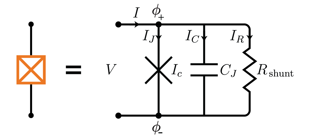
The supercurrent flowing through the junction is related to the Josephson phase, , by the current-phase relation:
| (1) |
where is the junction’s critical current. The Josephson phase, or the superconducting phase-difference across the junction, is essentially an angular measure of the flux along the junction branch, normalized so . As we will see below, it is more convenient here to work with node-fluxes instead of branch fluxes; the reduced branch flux, , is the difference of normalized node fluxes across the junction, in Fig. 1. The voltage across the junction, in Fig. 1, is related to the time derivative of the reduced flux by the AC Josephson relation:
| (2) |
The RCSJ model combines the current flowing in the junction Eq. (1) with those flowing in the resistance and capacitance, resulting in the following equation for the total current :
| (3) |
Substituting the AC Josephson relation in Eq. (2) into Eq. (3), yields the usual second-order differential equationBarone and Paterno (1982) for , however, the pair of first-order equations above is better suited for use in circuit simulators.
To capture this behavior in circuit simulation, ADS uses an auxiliary port on the junction schematic, and expresses the normalized node-flux difference across the junction, , as a fictitious voltage appearing on this port. Directly relating the phase difference across the junction to a voltage, such that V is equivalent to a phase difference, allows us to repurpose the simulator’s native solvers to account for fluxes in a ‘flux circuit’ just as it would account for voltages in an electrical circuit. The Josephson junction components (and the superconducting inductor components in Sec. III) serve to bridge between, and translate from, the electrical circuit to the flux circuit via Eq. (2). With this, the system can be represented solely through equations encompassing currents and voltages at distinct nodes. Equation (3) can then be used to capture the dynamics of the Josephson junction under the influence of external bias currents and voltages, resistance, and capacitance.
We will see below that exposing the node (either as a ground-referenced single-ended or as a floating differential voltage) on the ‘phi’ terminal of the junction models in ADS, allows the designer to enforce a phase- or flux-bias on the circuit, and opens the way to account for flux quantization conditions where appropriate in circuits containing junctions and inductors. Note that by convention, current flowing into the junction’s positive terminal corresponds to a positive phase-difference, and hence a positive .
It is worth noting here that Josephson junctions could be produced with a shunt resistance in order to control hysteresis effects. In Keysight ADS, when the model parameters are set to =0 and =0, it implies the absence of shunt resistance by default, resulting in a hysteretic device. The ADS models allow the specification of a shunt resistor either directly through the parameter, or indirectly through a specification of the McCumber damping factor such that is calculated as
| (4) |
In many cases, for unshunted junctions it is useful to set to some high, but finite resistance (e.g. ), to improve convergence of the simulation.
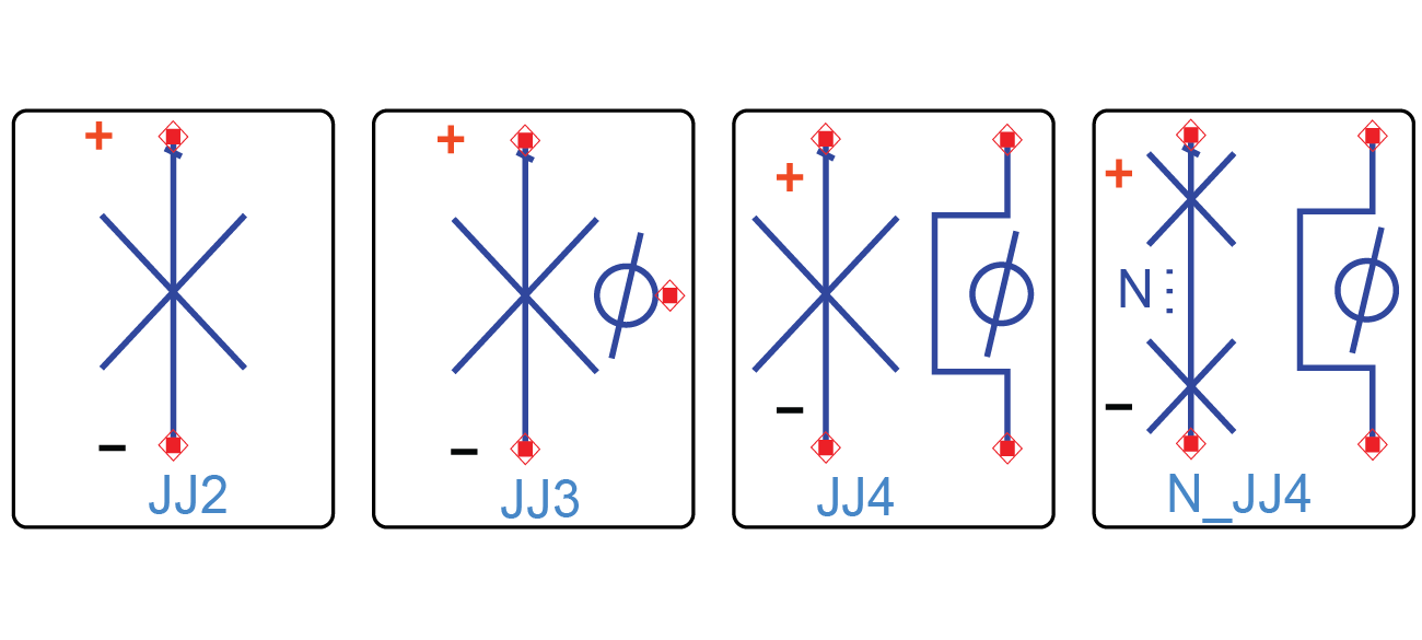
There are two basic behavioral models of the Josephson junctions in the Keysight ADS:
-
•
Two-terminal device (JJ2): follows the above RCSJ model while leaving the node floating and not exposed. In this case, the junction is driven by its supercurrent, and the phase adjusts according to Eq. (1).
-
•
Three-terminal device (JJ3): again follows the above RCSJ model but exposes the node. In this case, the junction can be driven from the node, effectively mimicking a flux biased junction. For the three-terminal device, the single-ended voltage at the node is ground-referenced.
To support the use of the flux nodes to implement the flux quantization condition into the simulated circuit, the following Josephson Junction models were added in the ADS 2025 release,
-
•
Four-terminal device (JJ4): here the flux has two terminals and the voltage drop between them results in that in turn controls the phase drop across the junction.
-
•
An array of identical junctions (N-JJ4): The voltage drop across the junctions is scaled by their number such that
(5) where is the voltage drop across the phi nodes of the individual Josephson junctions.
The various junction models and their schematic symbols are depicted in Figure 2. Note that JJ3 is equivalent to a JJ4 with its negative phase terminal connected to ground. Alternatively, JJ4 can be constructed from JJ3 by balancing its phi port using an ideal transformer.
III Inductance Models with Flux Nodes
Inductance plays a crucial role in inducing flux within superconducting loops, and this flux has to be accounted for if we want to accurately simulate flux quantizing circuits. A current flowing through an inductor will induce a flux across the inductor’s terminals. This can be accounted for by adding a “flux” port to the standard inductor model, and outputting a voltage volts across this second port.
Fig. 3(a) shows how a basic flux-aware inductor model could be constructed using a standard inductor and a current-controlled voltage source with a transimpedance of Ohms. Similar considerations also apply for the mutual-inductance transformer, with current in the primary coil of the transformer generating flux across the secondary coil. Note that while these models correctly adjust the flux in accordance with the current flowing through the inductance, they do not draw current in the inductor in response to a voltage being forced across the flux terminals.
Fig. 3(b) shows a more complete model following the ideas of Ref. Shiri et al., 2023. The model includes a voltage-controlled current source with transadmittance of S and an integrating capacitor fF to set with the appropriate normalization, where is the voltage across the inductor terminals. The inductor current then relates to the flux via the admittance matrix , .
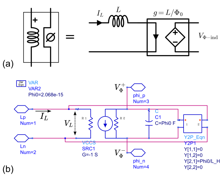
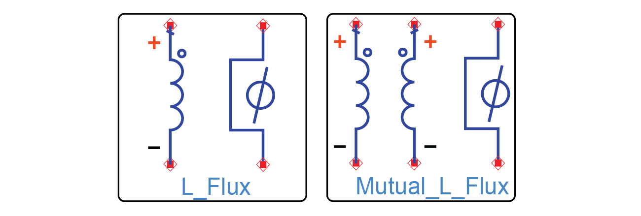
Keysight ADS 2025 introduces behavioral inductor and mutual inductance transformer models, depicted in Figure 4. The (L_Flux) model takes into account the flux across the inductance terminals, and has two modes of operation. The first mode, indicated by setting Mode=current driven, behaves similarly to Fig. 3(a) and solves for voltages such that the voltage drop across the inductor flux nodes is , and the voltage across the inductor terminals is the usual . The second mode, Mode=voltage driven, is more akin to Fig. 3(b) and solves for currents such that the current in the inductor is and the “current” into the flux port is . The two mode of operations for L_Flux are mutually exclusive. The comprehensive model of Fig. 3(b) can be easily constructed from standard library components but it doesn’t permit mutually exclusive operational modes for the inductance.
The Mutual-Inductance with Flux (Mutual_L_Flux) component in Fig. 4 describes a mutual inductance between a primary inductance and a secondary inductance with the extra flux nodes properly accounting for the induced flux with a corresponding voltage drop such that
| (6) |
It is important to recognize here that there will be induced flux even at DC – a unique feature for superconducting circuits. Meanwhile, currents and voltages in the arms of the mutual inductance device will follow
| (7) | ||||
| (8) |
where , , and , are the voltage, current in and , respectively.
IV Flux Quantization in ADS
As already mentioned, flux quantization arises naturally in transient simulation starting from a quiescent initial condition that sets all source, currents, and voltages to zero. In other simulation modalities, such as S-parameter, DC, AC, and HB analyses, flux quantization must be enforced externally. In ADS, having access to the junction phases via and inductor fluxes via , allows flux quantization to be expressed via an auxiliary circuit that constrains these fictitious voltages.
IV.1 Native flux quantization in transient simulation
Since flux quantization is a consequence of electromagnetism, transient simulations with ADS native standard components and a realistic Josephson junction model should correctly capture the salient physics in superconducting electronic circuits. To test this, we use the JJ3 model (see Figure 2) to construct an rf-SQUID and measure its phase vs flux relation.
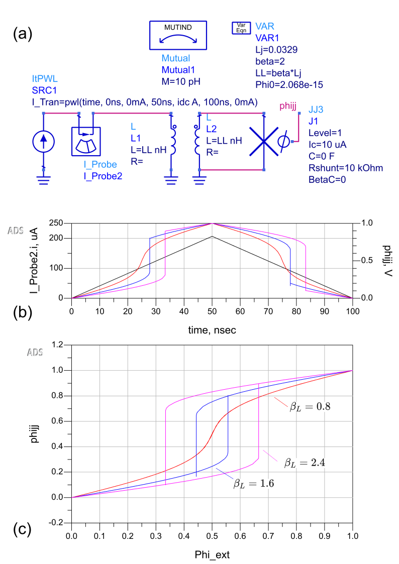
Fig. 5(a) shows the ADS circuit schematic used for this test. The rf-SQUID is the parallel connection of junction J1, having critical current A and inductor L2. The junction inductance is pH, and the linear inductance is , where is a parameter swept in the simulation. For the rf-SQUID is mono-stable, but for the rf-SQUID can store flux and its phase vs flux relation becomes hysteretic. Flux is induced into the rf-SQUID via a transformer having inductor L1 as its primary coil and L2 as the secondary, with a mutual inductance pH represented by the component Mutual1, and driven by a piece-wise-linear current source SRC1.
Figure 5(b) shows the current I_Probe2.i in the primary coil (left y-axis) as a function of time, ramping from an initial condition of to a maximum of idc A, corresponding to induced in the rf-SQUID loop: idc, and then ramping back to zero. The figure also shows, on the right axis, the voltage on the node phijj, corresponding to the junction phase. The three traces correspond to three different values of . Fig. 5(c) shows the voltage at the phijj node plotted vs the externally applied flux bias, Phi_ext for the three values of as indicated in the figure.
We observe the expected behavior of the rf-SQUID phase vs flux relation, which can be also calculated from
| (9) |
where is the external flux. For [red curve in Fig. 5(c)], the phase vs flux relation is continuous and mono-stable but nonlinear, with the junction phase reaching () at Phi_ext. At this value of flux bias the junction inductance diverges.
For higher values of , the rf-SQUID phase vs flux relation becomes hysteretic with the range of multistability increasing with , and the junction phase (phijj) jumps discontinuously when its values reach ,
| (10) |
For [blue in Fig. 5(c)] these jumps occur at Phi_ext and , and for (magenta in the figure) the jumps are at Phi_ext and as expected from Eqs. (10) and (9).
IV.2 Flux quantization with an auxiliary circuit
When a superconducting loop is subjected to an external magnetic field, the magnetic flux threading the loop is quantized in integer multiples of . For circuits with Josephson junctions and inductors, the flux quantization condition in the frequency domain boils down to a constraint on the sum of flux exhibited by the different components in the loop. Let’s consider the superconducting loop shown in Figure 6 that contains an arbitrary number of Josephson junctions and inductors, , and , respectively. In the presence of external flux , the sum of flux-induced phases around the loop should satisfy the relation
| (11) |
where and are the phase difference across Josephson junction and inductor , respectively. The integer is the number of flux quanta enclosed in the loop: this number can be zero when , but can change in circuits such as the dc-SQUID when the externally applied flux exceeds the above value; this change is associated with one of the junctions undergoing a phase slip, generating a voltage pulse across the junction whose time integral is exactly .
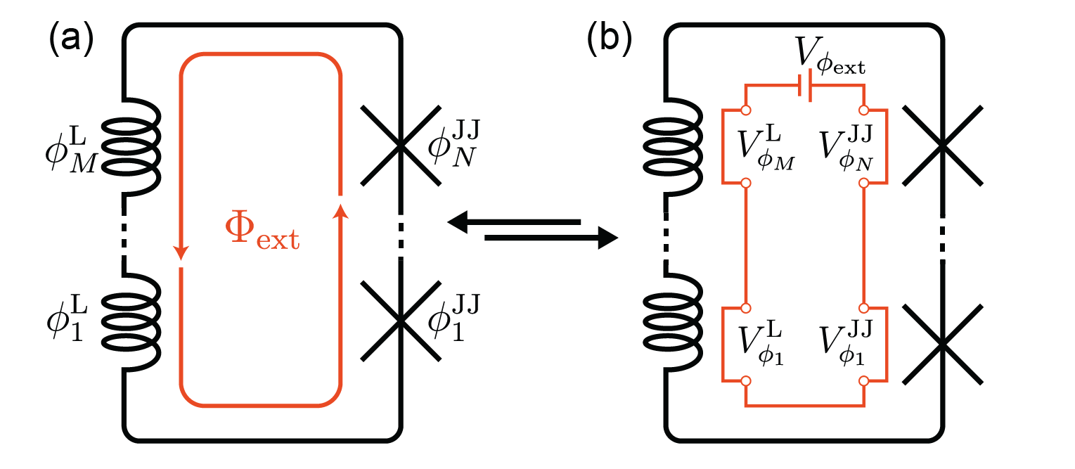
With the introduction of flux nodes for both the Josephson junctions and the inductors as was presented in Sections II and III, the flux condition can be translated to a voltage condition such that
| (12) |
where and are the voltage drops across the phi terminals of the Josephson junction and inductor , respectively. Fortunately, this condition can be fulfilled with an auxiliary flux loop through the Kirchhoff voltage law as shown in Figure 6. In principle, changing is equivalent to changing the external flux which in turn will change the bias of the different junctions in the loop and their equivalent inductance effectively tuning the circuit.
IV.2.1 Single junction: rf-SQUID
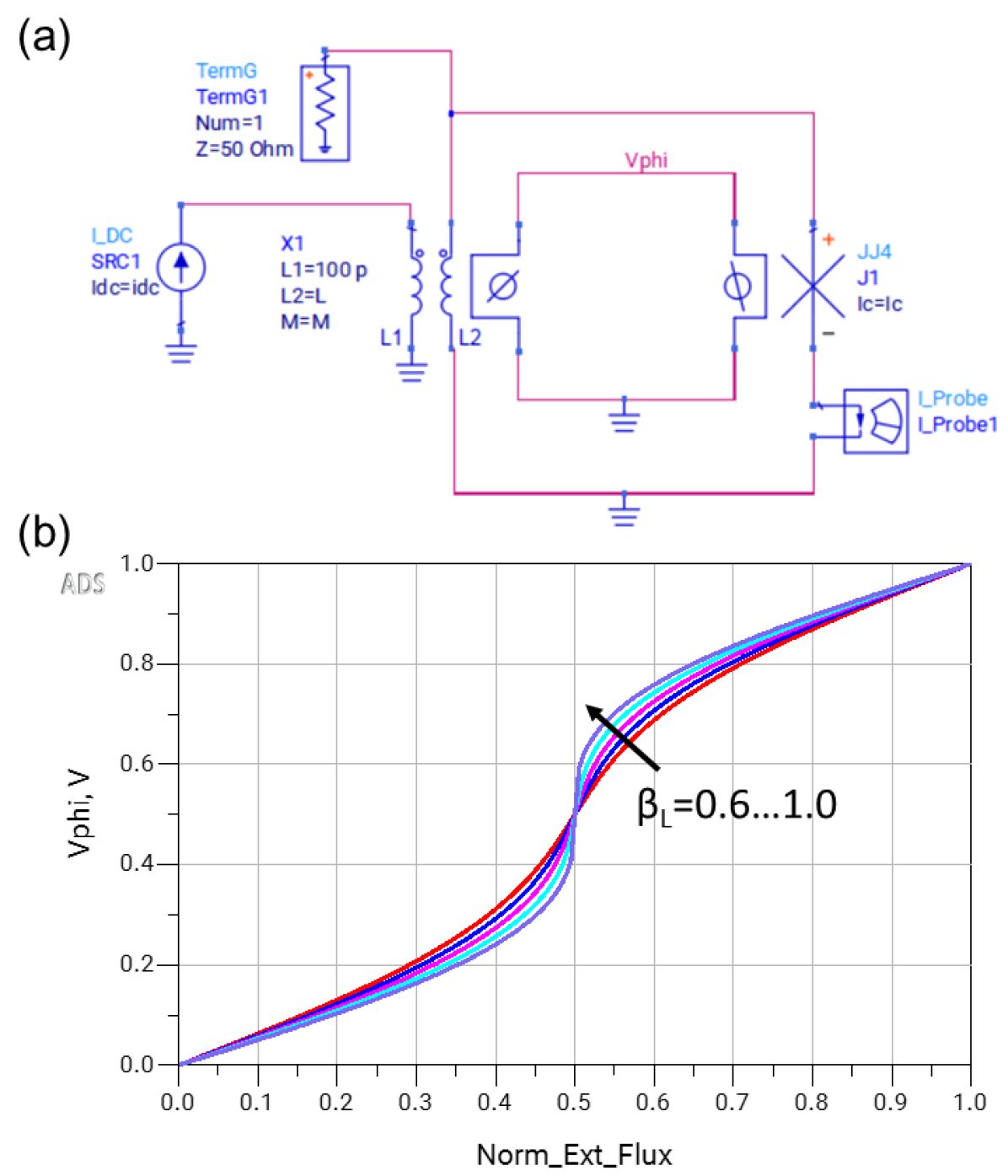
Figure 7 demonstrates how the flux quantization auxiliary circuit can be constructed for the simple case of an rf-SQUID. The schematic shown in Fig. 7(a) is using the JJ4 model and the secondary inductor of the Mutual_L_Flux model to form the rf-SQUID, and flux bias to the circuit is provided by the primary inductance of the Mutual_L_Flux component. In a DC simulation, the dc current source SRC1 driving the flux bias is outputting , and Norm_Ext_Flux is swept from 0 to 1.0. The flux quantization circuit is formed by connecting the phi port of the transformer in series with the phi port of the junction at the node Vphi. In the simulation, we sweep the value of from 0.6 to 1.0, and plot the voltage at the Vphi node (proportional to the junction phase) vs applied flux, Norm_Ext_Flux, in Fig. 7(b). The resulting phase vs flux relation as seen in the figure agrees with the theoretical expected behavior of Eq. (9).
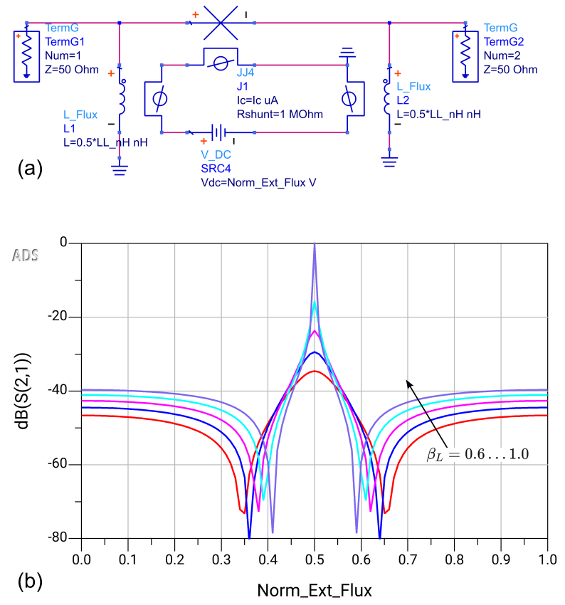
Alternatively, the flux threading the SQUID can be driven directly using a voltage source, as shown in Fig. 8(a). This circuit implements a tunable mutual coupler of the type used in Refs. Chen et al., 2014; Naaman et al., 2016: the coupling between the input and output ports can be nulled at a certain value of applied flux, for which the junction inductance diverges.
The schematic in Fig. 8(a) shows the linear inductor of the rf-SQUID split into two shunt branches bridged by a junction (A), forming a tunable inductive ‘pi’ circuit. The transmission through the structure at 5 GHz is shown in Fig. 8(b) as a function of the voltage output by the source SRC4 driving the flux quantization circuit (Norm_Ext_Flux) and for varying values of (which controls the value of the linear inductors in the circuit, as we have done in Fig. 5). We see that indeed there is a null in the transmission at specific -dependent values of the applied flux. The coupling near () is higher than that around integer normalize external flux, and becomes unity when , all in accordance with the device theory. The hysteretic regime of is generally avoided in this type of application.
IV.2.2 Two junctions: dc-SQUID
In a second simple example, we construct a dc-SQUID and extract its inductance from an S-parameter simulation. Fig. 9(a) shows the ADS schematic, where the SQUID is formed by the two JJ4 and two L_Flux blocks. The flux quantization circuit includes a dc voltage source, SRC3, to directly drive the external flux applied to the circuit.
We measure at GHz, calculate the SQUID input impedance seen from port 1, and from it calculate the SQUID inductance . The simulation is repeated for different values of applied flux, from to , as represented by the quantity Norm_Ext_Flux in Fig. 9(b).
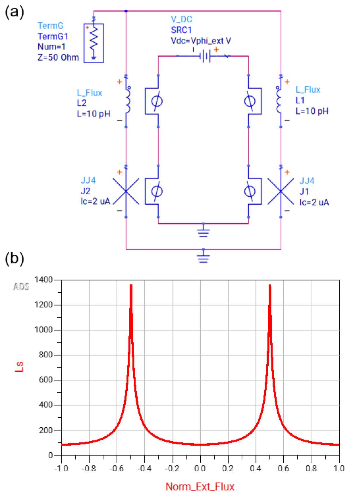
The dc-SQUID is a case where the number of flux quanta enclosed in the loop, in Eq. (11), can change. To capture this in the simulation, we assign an expression to the variable Vphi_ext, which sets the voltage of SRC3 and captures the modularity of the enclosed flux, using an ADS conditional statement and the modulus fmod() function.
    Vphi_ext =
      if Norm_Ext_Flux > 0
        then fmod(0.5+Norm_Ext_Flux,1)-0.5
        else fmod(-0.5+Norm_Ext_Flux,1)+0.5
      endif
Fig. 9(b) shows the simulated inductance in pH on the y-axis vs externally applied normalized flux, in agreement with the expected modulation curve of the SQUID. Because of the 20 pH linear inductance in the SQUID loop, the SQUID inductance does not truly diverge, and the range of modulation decreases for increasing as expected and observed in simulations (not shown).
When the dc-SQUID’s inductance vs flux modulation curve can become multi-valued and hysteretic, and any asymmetry in the junction critical currents or in the branch linear inductances will further complicate the dynamics. To simulate such situations, we usually prefer to perform transient analysis to understand the system’s stability regions; we can then perform small signal S-parameter or HB simulations in one of the stable regions.
V Compound circuits and arrays
Many microwave Josephson circuits developed in recent years involve compound SQUIDs and SQUID arrays, in which flux quantization must be accounted for across several (and often nested) superconducting loops. These compound devices, such as the superconducting nonlinear asymmetric inductive elementFrattini et al. (2017, 2018); Sivak et al. (2019); Miano et al. (2022) (SNAIL), the asymmetrically threaded SQUIDLescanne et al. (2020) (ATS), and the snake inductorBell et al. (2012); Naaman et al. (2017); White et al. (2023); Kaufman et al. (2023), arise in an attempt by designers to engineer the nonlinearity of Josephson microwave circuits to gain new functionality or improve their power handling. Here we will examine the SNAIL and Snake devices in the context of parametric amplification, and show how to construct flux-quantization aware schematics in ADS to model their behavior.
V.1 Kerr-free operation of a SNAIL amplifier
The SNAIL is a device composed of a series array of three Josephson junctions with critical current , in parallel with a smaller Josephson junction having a critical current of , where , as shown in Fig. 10(a). The design parameter , together with a flux bias to the SNAIL loop, give the designer control of the third- and fourth-order nonlinear terms in the device’s Hamiltonian. In particular, the device can be configured to feature a significant third-order nonlinearity that is useful for parametric amplification via a three-wave mixing process, while minimizing the fourth-order nonlinearity that is a contributor to saturation and harmonic distortionFrattini et al. (2017, 2018); Sivak et al. (2019).
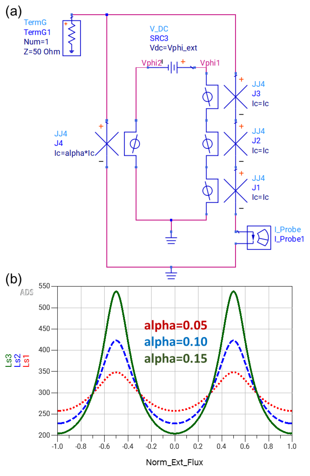
Figure 10(a) shows an ADS schematic of a SNAIL device composed of four JJ4 components. The flux quantization circuit is driven by a DC voltage source SRC3, setting the applied external flux to the SNAIL loop. Fig. 10(b) shows the simulated inductance of the SNAIL, computed from in an S-parameter analysis, as a function of flux bias and for various values. The inductance varies periodically with flux, and modulates as expected with a range that increases with .
In Fig. 11, we implement a parametric amplifier based on a series array of 20 SNAIL elements (with all junction ) embedded at the current antinode of a half-wave transmission line resonatorFrattini et al. (2018). Fig. 11(a) shows the circuit schematic; the SNAIL array with A and is the sub-circuit X1 in the figure, and transmission lines TL1 and TL2 form the resonator, whose frequency is tunable with flux between approximately 6 and 7.5 GHz. The signal is coupled into and out of the amplifier via capacitor C1, and the pump is fed via capacitor C2. Component values are shown in the figure, and are based on ‘device C’ in Ref. Frattini et al., 2018.
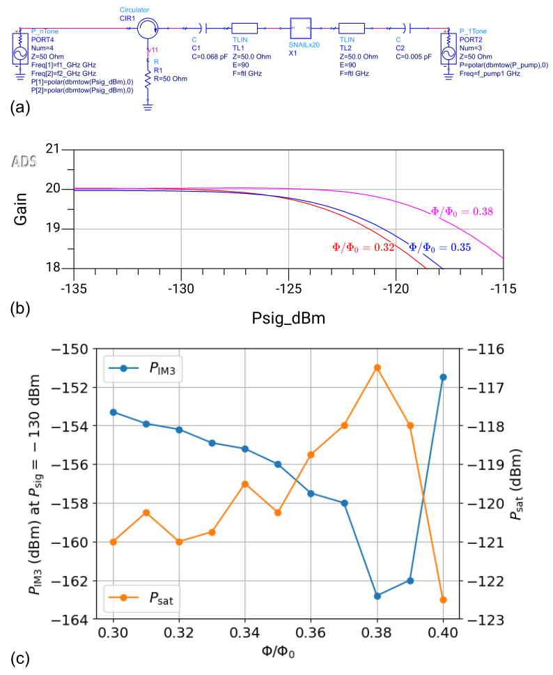
To test the SNAIL model, we examine the so called ‘Kerr-free’ pointSivak et al. (2019); Frattini et al. (2018) of the SNAIL parametric amplifier by performing harmonic balance simulations with 2-tone drive, and measuring the amplifier’s saturation power and 3rd order intermodulation products. At the flux bias corresponding to the Kerr-free point, the fourth-order nonlinearity of the amplifier is minimized giving rise to higher saturation power and lower harmonic distortion. At each simulated flux bias, we adjust the pump frequency to be twice the resonant frequency of the SNAIL-loaded resonator, and adjust the pump power to obtain 20 dB of gain. The two signal tones are separated by 100 kHz and are centered at a 500 kHz detuning from the center frequency of the resonator.
Fig. 11(b) shows the simulated gain vs input signal power (per tone) for 3 different flux biases. We observe the familiar gain compression as the signal power is increased, with a flux-dependent compression point. Near , the amplifier’s saturation power reaches a maximum of dBm per tone, or dBm of total power, in reasonable agreement with the experiments in Ref. Frattini et al., 2018.
Fig. 11(c) shows (orange, right axis), and the power in the 3rd order intermodulation product (blue, left axis). was recorded for input signal power of dBm, well below saturation. The figure clearly shows a maximum in the saturation power and a coincident minimum in the 3rd order intermodulation product power near , which is identified as the Kerr-free operating point in Ref. Frattini et al., 2018 for a device with similar parameters.
V.2 Snake rf-SQUID array and the Lumped-Element Snake Amplifier
The ‘snake’ is a nonlinear inductance made with an array of interleaving rf-SQUIDs, as shown in Fig. 12(a). It is composed of a meandering spine of alternating linear inductors, and , and each of the meanders is bridged by a Josephson junction with inductance , such that . This structure is based on an array proposed in Ref. Bell et al., 2012, and was used (with linear inductances replacing Josephson junctions in the spine) in Ref. Naaman et al., 2017 as a high saturation power Josephson nonlinear element.
Flux is quantized in each of the rf-SQUID loops in the array. If is the normalized flux due to current in inductance , is the flux across , and is the flux across the junction, then in each loop containing two inductors, an inductor, and a junction, we have . The array is driven by imposing a phase difference across the -stage array [see Fig. 12(a)], such that .
In ADS, we can define a sub-circuit to represent a 2-junction stage of the snake inductor, as highlighted with a dashed box in Fig. 12(a). The schematic of that sub-circuit is shown in Fig. 12(b), and uses the JJ4 component (with ) and the L_Flux model of Fig. 3(b). In the figure, the signal path is indicated with black wires, and the auxiliary flux quantization circuit is indicated with blue wires. In the rf-SQUID loop (green dashed arrow), the voltages associated with the flux across the inductors, are summed and applied across the junction terminals. The flux across the 2-junction stage is propagated from the input to the output phi terminals of the block, advancing as indicated by the dashed orange arrow. The snake array can then be constructed by connecting a number of these sub-circuits in series, and terminating the array’s last stage with an additional L_Flux component.
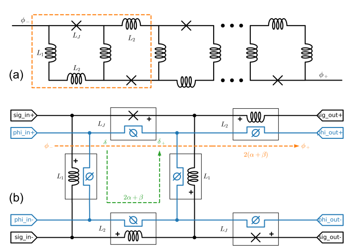
Figure 13(a) shows a nonlinear inductance element built from 20 such sub-circuits, a total of 40 junctions, arranged in two parallel arrays of rf-SQUID stages each. We call the common mode of this array the ‘signal’ mode. The differential ‘circulating’ mode of the circuit includes a superconducting transformer (two Mutual_L_Flux components in series in the figure), which is driving a flux bias to the circuit via a mutual inductance . The particular snake array shown in Fig. 13(a) is modeled according to that used in Refs. White et al., 2023; Kaufman et al., 2023, with pH, pH, and junction A.
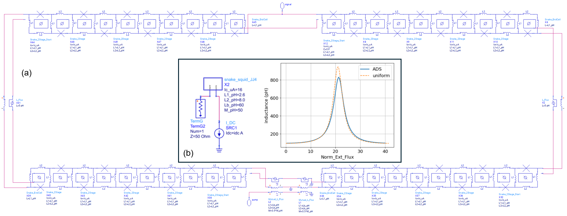
We perform S-parameter simulations at a fixed frequency of 5 GHz, and with a swept applied external flux. Similar to what we have done in Sec. IV.2.2, we extract the array’s inductance as seen from the signal port from the simulated , and plot this inductance vs flux bias in Fig. 13(b), solid blue trace. The simulated schematics is shown in panel (b) inset, with sub-component X2 representing the snake array of panel (a), and current source SRC1 providing a dc flux bias across the entire 40-squid array by outputting .
Fig. 13(b) additionally shows, in dashed orange line, the calculated inductance
| (13) |
where is the equilibrium phase across each of the junctionsNaaman et al. (2017); White et al. (2023), and where the flux axis is scaled to account for the bias transformer inductance according to Eq. (S12) in Ref. White et al., 2023 appendix. Eq. (13) assumes the snake array is uniform and perfectly periodic, and therefore represents an approximation neglecting any nonuniformity of the currents arising from the finite extent of the array. As we can see from Fig. 13(b), the uniform-array approximation is in reasonable agreement with the simulation results. This example shows that while a closed-form approximation is useful in designing such devices, only circuit simulations can fully capture subtleties that can be important to the exact flux dependence of the inductance, especially in the context of parametric amplification and higher-order nonlinearities that contribute to intermodulation distortion and saturation.
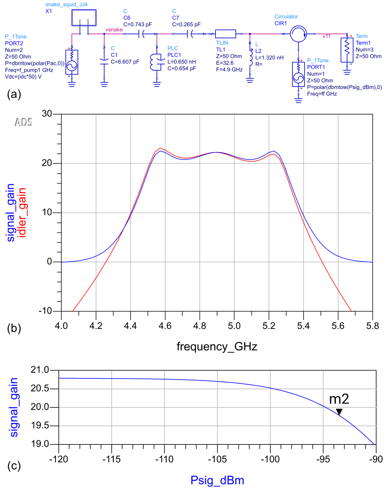
Figure 14(a) shows an ADS schematic of the lumped-element snake amplifier (LESA) demonstrated in Ref. Kaufman et al., 2023. This is a broad-band matchedNaaman and Aumentado (2022) Josephson parametric amplifier based on a 3-pole Chebyshev matching network, and designed to have high saturation power by using the snake inductor as its nonlinear element. The schematic uses the same snake component shown in Fig. 13(a) and (c), pumped and biased by source PORT2 in the figure, outputting dBm at GHz (modulation amplitude of ), and with a DC level set to bias the snake with a flux of . The input signal, with input power of Psig_dBm, is provided by PORT1 through an ideal circulator. The power delivered to the load Term1 is measured in a harmonic balance simulation at both the signal frequency, , and the idler frequency, . All component values are given in Fig. 14(a).
Fig. 14(b) shows the signal gain in dB (blue), extracted from the HB simulation from the voltage at the node v11, using the ADS mix() function,
signal_gain=dBm(mix(v11, {0, 1}))-Psig_dBm
where the indexes {0, 1} indicate a frequency that is the sum of the zeroth harmonic of the pump and the first (fundamental) harmonic of the signal. The idler gain (red) can be extracted similarly by using indexes {1, -1}, selecting a frequency that is the difference between the pump and signal fundamentals frequencies. We see in the figure that the small-signal ( dBm) gain of the LESA amplifier is just over 20 dB, with approximately 1 dB gain ripple, and a bandwidth exceeding 600 MHz.
Fig. 14(c) shows a HB simulation in which the signal frequency was fixed at 4.7 GHz and the signal power was swept. We see the familiar gain compression phenomenon, with a 1-dB input compression power of dBm (indicated in the figure by marker m2, in agreement with the experimentally measured LESA devices in Ref. Kaufman et al., 2023.
VI Working with flux models
Representing the flux in a circuit as a fictitious voltage requires some care when working with flux-aware models. In inductance models such as the one in Fig. 3(a), where the flux port is driven by what is essentially an ideal voltage source with zero internal resistance, a case where such inductors are placed in parallel could result in either voltage source attempting to bias an effective short circuit. The simulator will attempt a solution with unusually large currents flowing through the flux loop and will often fail, or may attempt to ‘fix’ the problem by adding a small series resistance, which will then change the applied flux in the circuit. Such topolgies should be avoided, or otherwise the model of Fig. 3(b) should be used instead. Additionally, the flux port and the signal port of the inductor and junction components are not independent, and nonsensical results could be obtained if we build a circuit that attempts, for example, to both current-bias and phase-bias the component simultaneously. The L_Flux models shipped with ADS can help designers guard against these unintended behaviors by exclusively limiting the model’s operation to either a voltage (flux) bias mode or a current bias mode.
The use of a voltage source to implement a flux bias in a circuit can also tempt a designer to simulate circuits that cannot be physically implemented. For example, in simulation it would be perfectly legal to directly phase bias a junction that is not embedded in a superconducting loop, essentially using the source as a ‘flux battery’. However, no such device exists in the physical world. Direct flux bias is only valid within a context of a superconducting loop, as we demonstrated in Figs. 8-10. Biasing a physical design via a mutual transformer as in Figs. 7 and 12 is in many cases preferred, as it anchors the simulation in physical reality. On the other hand, direct access to a supreconducting circuit’s flux nodes offers some new opportunities in characterizing devices in simulation—enabling, for example, a direct probe of a device’s nonlinearity, current-phase relation, or inductance flux-tuning curve in isolation.
VII Conclusions
We have introduced Josephson junction and inductance models in Keysight ADS, which explicitly account for the node fluxes at the devices’ terminals, and expose them on the device schematic symbols as auxiliary port. Using these models, it is now possible to enforce flux quantization conditions in ADS simulations of superconducting devices—this is a critical feature whose absence thus far has limited the usability of modern EDA tools in microwave superconducting circuit design. We have shown a few examples of how such circuits can be constructed, going from simple devices like the rf- and dc-SQUID to multi-junction compound devices and arrays. We validated the models and their usage in DC, S-parameter, and harmonic balance simulations, against theoretical results as well as published experimental data. In particular, we demonstrated an important use case in the simulation of Josephson parametric amplifiers, and reproduced in simulation some key experimental results from SNAIL and LESA devices. We are excited by the opportunities that these methods offer to modernize the simulations, and accelerate the development of microwave superconducting electronic devices and circuits.
References
- Barone and Paterno (1982) A. Barone and G. Paterno, Physics and Applications of the Josephson Effect, A Wiley-interscience publication (Wiley, 1982).
- Van Duzer and Turner (1999) T. Van Duzer and C. Turner, Principles of Superconductive Devices and Circuits (Prentice Hall, 1999).
- Krantz et al. (2019) P. Krantz, M. Kjaergaard, F. Yan, T. P. Orlando, S. Gustavsson, and W. D. Oliver, “A quantum engineer’s guide to superconducting qubits,” Applied Physics Reviews 6, 021318 (2019).
- Likharev and Semenov (1991) K. Likharev and V. Semenov, “RSFQ logic/memory family: a new Josephson-junction technology for sub-terahertz-clock-frequency digital systems,” IEEE Transactions on Applied Superconductivity 1, 3–28 (1991).
- Benz and Hamilton (2004) S. Benz and C. Hamilton, “Application of the Josephson effect to voltage metrology,” Proceedings of the IEEE 92, 1617–1629 (2004).
- Qiu et al. (2023) J. Y. Qiu, A. Grimsmo, K. Peng, B. Kannan, B. Lienhard, Y. Sung, P. Krantz, V. Bolkhovsky, G. Calusine, D. Kim, A. Melville, B. M. Niedzielski, J. Yoder, M. E. Schwartz, T. P. Orlando, I. Siddiqi, S. Gustavsson, K. P. O’Brien, and W. D. Oliver, “Broadband squeezed microwaves and amplification with a Josephson travelling-wave parametric amplifier,” Nature Physics 19, 706–713 (2023).
- Mukhanov (2011) O. A. Mukhanov, “Energy-efficient single flux quantum technology,” IEEE Transactions on Applied Superconductivity 21, 760–769 (2011).
- Herr et al. (2011) Q. P. Herr, A. Y. Herr, O. T. Oberg, and A. G. Ioannidis, “Ultra-low-power superconductor logic,” Journal of applied physics 109 (2011).
- Takeuchi et al. (2022) N. Takeuchi, T. Yamae, C. L. Ayala, H. Suzuki, and N. Yoshikawa, “Adiabatic quantum-flux-parametron: A tutorial review,” IEICE Transactions on Electronics 105, 251–263 (2022).
- Whiteley (1991) S. Whiteley, “Josephson junctions in SPICE3,” IEEE Transactions on Magnetics 27, 2902–2905 (1991).
- Naaman et al. (2019) O. Naaman, D. Ferguson, A. Marakov, M. Khalil, W. Koehl, and R. Epstein, “High saturation power Josephson parametric amplifier with GHz bandwidth,” in 2019 IEEE MTT-S International Microwave Symposium (IMS) (IEEE, 2019) pp. 259–262.
- Malnou et al. (2024) M. Malnou, B. Miller, J. Estrada, K. Genter, K. Cicak, J. Teufel, J. Aumentado, and F. Lecocq, “A traveling-wave parametric amplifier and converter,” arXiv preprint arXiv:2406.19476 (2024).
- Ranadive et al. (2024) A. Ranadive, B. Fazliji, G. L. Gal, G. Cappelli, G. Butseraen, E. Bonet, E. Eyraud, S. Böhling, L. Planat, A. Metelmann, et al., “A traveling wave parametric amplifier isolator,” arXiv preprint arXiv:2406.19752 (2024).
- O’Brien and Peng (2022) K. O’Brien and K. Peng, “JosephsonCircuits.jl,” (2022), https://github.com/kpobrien/JosephsonCircuits.jl.
- Peng et al. (2022) K. Peng, R. Poore, P. Krantz, D. E. Root, and K. P. O’Brien, “X-parameter based design and simulation of Josephson traveling-wave parametric amplifiers for quantum computing applications,” in 2022 IEEE International Conference on Quantum Computing and Engineering (QCE) (2022) pp. 331–340.
- Choi et al. (2023) J. Choi, M. I. Abdelrahman, D. Slater, T. Parker, P. Krantz, P. Sohn, M. A. Hassan, and C. Mueth, “QuantumPro: An integrated workflow for the design of superconducting qubits using Pathwave Advanced Design System (ADS),” in 2023 IEEE International Conference on Quantum Computing and Engineering (QCE), Vol. 02 (2023) pp. 224–225.
- Shiri et al. (2023) D. Shiri, H. R. Nilsson, P. Telluri, A. F. Roudsari, V. Shumeiko, C. Fager, and P. Delsing, “Modeling and harmonic balance analysis of parametric amplifiers for qubit read-out,” arXiv preprint arXiv:2306.05177 (2023).
- Kaufman et al. (2023) R. Kaufman, T. White, M. I. Dykman, A. Iorio, G. Sterling, S. Hong, A. Opremcak, A. Bengtsson, L. Faoro, J. C. Bardin, et al., “Josephson parametric amplifier with Chebyshev gain profile and high saturation,” Physical Review Applied 20, 054058 (2023).
- White et al. (2023) T. White, A. Opremcak, G. Sterling, et al., “Readout of a quantum processor with high dynamic range Josephson parametric amplifiers,” Applied Physics Letters 122, 014001 (2023), https://doi.org/10.1063/5.0127375 .
- Frattini et al. (2017) N. Frattini, U. Vool, S. Shankar, A. Narla, K. Sliwa, and M. Devoret, “3-wave mixing Josephson dipole element,” Applied Physics Letters 110 (2017).
- Chen et al. (2014) Y. Chen, C. Neill, P. Roushan, N. Leung, M. Fang, R. Barends, J. Kelly, B. Campbell, Z. Chen, B. Chiaro, et al., “Qubit architecture with high coherence and fast tunable coupling,” Physical review letters 113, 220502 (2014).
- Naaman et al. (2016) O. Naaman, M. Abutaleb, C. Kirby, and M. Rennie, “On-chip Josephson junction microwave switch,” Applied Physics Letters 108 (2016).
- Frattini et al. (2018) N. E. Frattini, V. V. Sivak, A. Lingenfelter, S. Shankar, and M. H. Devoret, “Optimizing the nonlinearity and dissipation of a SNAIL parametric amplifier for dynamic range,” Phys. Rev. Appl. 10, 054020 (2018).
- Sivak et al. (2019) V. Sivak, N. Frattini, V. Joshi, A. Lingenfelter, S. Shankar, and M. Devoret, “Kerr-free three-wave mixing in superconducting quantum circuits,” Physical Review Applied 11, 054060 (2019).
- Miano et al. (2022) A. Miano, G. Liu, V. Sivak, N. Frattini, V. Joshi, W. Dai, L. Frunzio, and M. Devoret, “Frequency-tunable Kerr-free three-wave mixing with a gradiometric SNAIL,” Applied Physics Letters 120 (2022).
- Lescanne et al. (2020) R. Lescanne, M. Villiers, T. Peronnin, A. Sarlette, M. Delbecq, B. Huard, T. Kontos, M. Mirrahimi, and Z. Leghtas, “Exponential suppression of bit-flips in a qubit encoded in an oscillator,” Nature Physics 16, 509–513 (2020).
- Bell et al. (2012) M. Bell, I. Sadovskyy, L. Ioffe, A. Y. Kitaev, and M. Gershenson, “Quantum superinductor with tunable nonlinearity,” Physical review letters 109, 137003 (2012).
- Naaman et al. (2017) O. Naaman, J. Strong, D. Ferguson, J. Egan, N. Bailey, and R. Hinkey, “Josephson junction microwave modulators for qubit control,” Journal of Applied Physics 121, 073904 (2017).
- Naaman and Aumentado (2022) O. Naaman and J. Aumentado, “Synthesis of parametrically coupled networks,” PRX Quantum 3, 020201 (2022).