Millimeter-Scale Ultra-Low-Power Imaging System for Intelligent Edge Monitoring
Abstract.
Millimeter-scale embedded sensing systems have unique advantages over larger devices as they are able to capture, analyze, store, and transmit data at the source while being unobtrusive and covert. However, area-constrained systems pose several challenges, including a tight energy budget and peak power, limited data storage, costly wireless communication, and physical integration at a miniature scale. This paper proposes a novel 6.775mm imaging system with deep-learning and image processing capabilities for intelligent edge applications, and is demonstrated in a home-surveillance scenario. The system is implemented by vertically stacking custom ultra-low-power (ULP) ICs and uses techniques such as dynamic behavior-specific power management, hierarchical event detection, and a combination of data compression methods. It demonstrates a new image-correcting neural network that compensates for non-idealities caused by a mm-scale lens and ULP front-end. The system can store 74 frames or offload data wirelessly, consuming 49.6W on average for an expected battery lifetime of 7 days.
1. Introduction
Miniaturized Internet-of-Things (IoT) systems have unique advantages over larger devices due to their ability to provide contextual information at the data source. They can be particularly advantageous in healthcare scenarios, where medically implanted devices need to be non-obtrusive for long-term in vivo monitoring (Lee et al., 2019), and in environmental and animal monitoring applications, where larger instrumentation could disturb the target species or be unable to capture hyper-local data (Bick et al., 2021)(Iyer et al., 2020).
Embedded vision systems have the potential to transform application spaces, such as industrial monitoring particularly in remote or hazardous locations. In spite of these benefits, size-constrained sensing systems pose several fundamental challenges, all of which are exacerbated by using a data-intensive and power-hungry visual sensing modality. The following technical challenges unique to mm-scale systems are tackled in our proposed system:
1) Millimeter (mm)-scale size: Designing a highly area constrained system requires integrating ultra-low power (ULP) ICs and assembling them to minimize system size. A mm-scale battery is needed to maintain small system dimension, imposing tight energy and peak power constraints.
2) Constrained energy budget and peak current: Millimeter-scale batteries have limited capacities (1-50 mAh) and stringent peak current constraints whereas always-on image sensors have high power consumption, particularly compared to other sensing modalities such as audio. Imaging systems often include computation- and data-intensive digital signal processing and analytic algorithms to perform advanced tasks such as image compression and object/event detection. Deep neural networks (DNNs) can enhance the accuracy of these algorithms but often with the expense of higher number of operations and stored parameters.
3) Limited data storage: Unlike other scalar sensing modalities, raw image data has a significant memory footprint of 3.7Mb per VGA (6404803 pixel) frame. A mm-scale system will have a limited amount of on- and off-chip memory available, limiting the storage of image data and the complexity of the algorithms used.
4) Costly wireless communication: ULP wireless communication imposes an overall high energy cost due to low data rates (1Mbps), making it inefficient to offload large volumes of data. Commercial off-the-shelf Bluetooth low energy wireless solutions provide a higher data rate but require a reference crystal and matching antenna with relatively high active power consumption of 10 mW, placing it outside our system constraints.
5) Non-idealities from mm-scale lens and ULP front-end: Though using a mm-scale lens and ULP imaging front-end enable unobtrusive long-term operation, the resulting images are susceptible to color and geometric distortions. DNN algorithms that have been trained on high quality image datasets suffer significant performance degradation when applied to mm-scale IoT systems.
To address these challenges, work has been done on low-power image sensors (Ji et al., 2016)(Morishita et al., 2021), ULP processors (Rossi et al., 2021)(Smets et al., 2019) and mixed-signal vision ICs (Lefebvre et al., 2021)(Xu et al., 2021), low-power wireless communication (Song et al., 2020)(Thijssen et al., 2020), efficient neural accelerators (Jia et al., 2021)(Lu et al., 2021), and optimizing machine learning algorithms for embedded applications (Ajani et al., 2021). However, limited prior work has combined these approaches into a functional system. Prior demonstrated systems (Balasubramanian et al., 2018)(Iyer et al., 2020)(Josephson et al., 2019)(Kim et al., 2014)(Naderiparizi et al., 2017) either do not incorporate edge intelligence or do not meet the area/power-constraints that motivate this paper.
This paper proposes and demonstrates a fully integrated mm-scale imaging system with deep-learning and image processing capabilities, which is the first of its kind. By using a combination of techniques specific to ULP tiny-IoT systems that tackle the above challenges, we achieve a lifetime of 7 days without recharging the battery and an overall average power consumption of 49.6W. Long-term sustained operation may be achieved by using the system’s energy harvesting IC to recharge the battery.
2. System Description
2.1. Stacked custom ICs
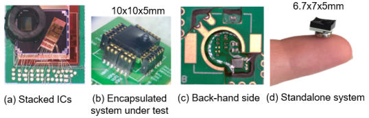
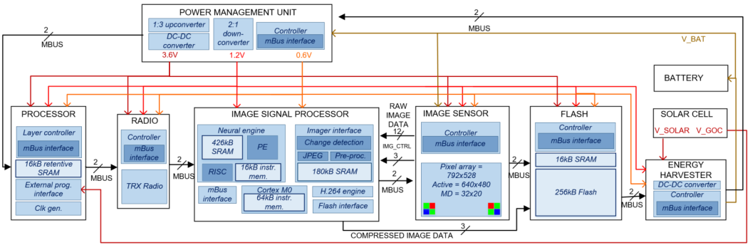
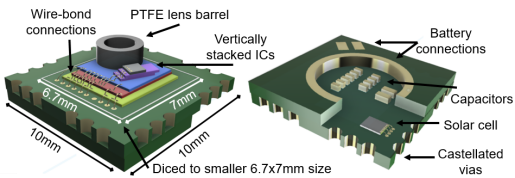
The system uses un-packaged and thinned (150m) ULP ICs from a family of custom chips that are prior-designed to be vertically stacked and interconnected by attaching wire-bonds between IC bond pads as shown in Fig. 1a. This method increases the number of ICs that can be integrated in the same footprint in comparison to traditional planar 2D chip-to-chip connection on a PCB, allowing the system to achieve a 6.775mm size and 460mg weight (battery included). The integrated system (Fig. 1 and Fig. 3) consists of:
1) A base-layer: It integrates the following into a single IC die to reduce stacking height and wire bonding complexity.
-
•
A master controller, containing a Cortex-M0 microprocessor and 16kB SRAM, that is designed for ULP operation, provides the clock and acts as a bus mediator for the open-source ULP bus protocol mBus (Pannuto et al., 2015), used for inter-layer communication.
-
•
A power management unit that generates 0.6V, 1.2V and 3.6V domains from a single battery voltage in the range of 0.9-4V, and maintains high conversion efficiency under loads ranging from nW to hundreds of W (Jung et al., 2016).
-
•
A radio IC that uses energy-efficient sparse pulse position modulation consuming ¡70W of average active power (Chen et al., 2016). It is connected to a metal trace loop antenna integrated within the PCB, and uses a carrier frequency of 1.2GHz and sampling frequency of 240kHz generated by an on-chip oscillator without a crystal reference.
2) A ULP image sensor layer: It supports motion-triggered 12-bit VGA image capture and also near-pixel motion detection on a sub-sampled 3220 pixel frame at a maximum rate of 170 fps (Choo et al., 2019).
3) A ULP image signal processing (ISP) layer: It is a revised version of (An et al., 2020), that performs on-the-fly JPEG (de)compression, optical-black pixel calibration, de-Bayering, RGB-to-YUV conversion, and scene change detection when an image is streamed in. It has a H.264 compression engine and 180kB of SRAM to store compressed frames on-chip. A neural engine (NE) with a peak efficiency of 1.5 TOPS/W enables DNN-based frame analysis, and has 426kB SRAM and a custom RISC-like processor. An internal ARM Cortex-M0 microprocessor orchestrates these components. The ISP’s memory banks have separately-controllable power-gating switches to reduce leakage energy for non-retentive data.
4) Two stacked, custom ultra-low-leakage flash layers: They provide a total of 16kB SRAM storage and 256kB flash storage with 11pJ/bit read energy and pW sleep power (Dong et al., 2017).
5) An energy harvester layer: It is designed to be supplied by a low-voltage source that has a configurable conversion ratio to increase harvesting efficiency for a range of input voltages (Jung et al., 2014).
6) A solar cell layer: It is for energy harvesting and a global optical communication (Moon et al., 2019).
7) A 3V 3.4mAh 5.81.8mm rechargeable lithium battery: It weighs 130mg with 150A maximum continuous discharge current and 10A standard discharge current.
8)A polytetrafluoroethylene (PTFE) tube: It is used as a lens barrel, housing a medical endoscopic lens.
Layers are connected in a daisy-chain configuration and forward mBus transactions between a transmitting and a receiving layers as shown in Fig. 2. The ISP’s image interface connects directly to the image sensor IC pads for raw data and synchronization signals. The ISP’s flash interface allows it to stream (de)compressed image data directly to flash. The power management unit generates 3 power domains that are distributed throughout the system. The battery is recharged by the harvester connected to the solar cell layer.
2.2. System design and integration
The system uses two 4 layer 10100.8mm PCBs. The front of the first PCB is used for wire-bonding the stacked ICs whereas passive components and the solar cell layer are placed on the back (Fig. 1c). The second PCB provides spacing between passive components and the battery so these can be placed above each other.
Since code development and debug on miniature systems is extremely difficult due to limited physical access, we include castellated vias on the outer rims of the system to expose internal signals that connect to compression contacts in our test setup (Fig.1b). Fig. 3 shows a white outline where the system can be diced a second time into an even smaller form-factor of 6.775mm (Fig. 1d). With this smaller size, the system loses all exposed probe contacts for debugging and monitoring, thus must be wirelessly programmed through an optical communication interface using the solar cell.
Fig. 1 shows a completed assembly, where the stacked ICs have been encapsulated in black epoxy to block out light due to ULP IC’s light-sensitivity. The solar cell is encapsulated with clear epoxy to be exposed to light. The image sensor is also left exposed by attaching the PTFE lens barrel over it prior to encapsulation.
3. System Demonstration
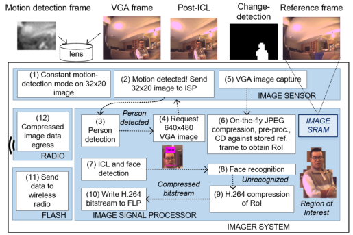
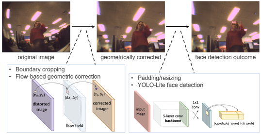
The system is fully programmable for various applications. As a driving application example, we demonstrate the system for home-surveillance as depicted in Fig. 4. In the demonstrated scenario, the image sensor captures highly sub-sampled (32201 pixel) frames at a rate of 1fps and performs motion detection on-chip. When motion is detected, the ISP receives the sub-sampled frame and performs DNN-based person detection. If a person is not detected, the system returns to continuous motion-detection mode. Otherwise, a VGA frame is taken by the image sensor and streamed to the ISP, which performs image pre-processing, JPEG compression and change detection on the scene by comparing it to a stored reference frame to obtain a pruned (non-rectangular) region of interest (RoI).
Then, the VGA image is corrected for geometric distortion and resized for YOLO-Lite-based face detection. It is a one-shot object detection and localization DNN based on (Huang et al., 2018), widely researched for embedded vision systems, and we customized it to satisfy the system constraints. If a face is not detected, the system returns to the continuous motion-detection mode. Otherwise, the scene is analyzed by performing DNN-based face recognition. The image RoI is H.264 compressed and stored in the system’s flash layer only when a face is not recognized (i.e., a possible intruder) for optional wireless transmission to a custom gateway. The VGA frame containing an intruder is reconstructed offline.
4. Energy Minimization Techniques
The chosen mm-scale battery has a limited capacity, making power management crucial to achieve a standalone system with a reasonable operating lifetime. This is particularly challenging for always-on imaging systems, where power consumption is dominated by the continuously running image sensor. Performing DNN-based analysis is costly due to both the computation energy and the mega-bytes of DNN parameters stored on-/off-chip. However, intelligent DNN-based classifications on the edge is crucial in order to reduce wireless data offloading, which consumes 15nJ/b and can dominate the system’s energy consumption for large data volumes if not trimmed by DNN-based edge processing.
4.1. Dynamic energy-efficient modes
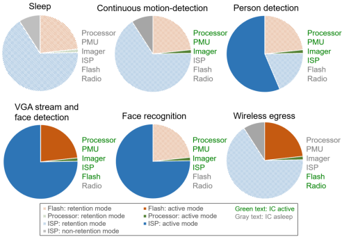
Most ICs in the proposed system are duty-cycled to optimize the system’s power consumption for the chosen application. Fig.5 shows the power breakdown of each mode. For instance, flash ICs are set to sleep during motion monitoring, image capture, and DNN-based scene analysis, consuming only 0.003W. ISP allows for fine-grained software control of its SRAM banks, which can be in low-power retention mode without loss of data. The NE SRAM is partitioned into 7 variably-sized blocks that can be selectively power-gated to reduce leakage power consumption according to DNN storage requirements. The H.264 engine and image interface memory also have this capability. For example, when the system is in continuous motion-detection mode, the 430kB ISP memory can be power-gated, reducing the leakage power by 1.8. The power management unit is adjusted at each mode to maximize the efficiency for the dynamic load by modifying current draw, frequency control and up/down conversion ratio, achieving an average efficiency of 64%.
4.2. Hierarchical event detection
A hierarchical event detection (HED) algorithm is employed to prune out irrelevant events that would otherwise wastefully consume energy, particularly when offloading data without determining its value to the user. This approach uses efficient motion detection in the imager front-end and lower complexity DNN-analysis in the ISP back-end to reduce the frequency at which costly VGA images and higher-complexity DNN algorithms are performed, significantly decreasing the system’s average power/energy.
While the image sensor IC is in motion-detection mode, which is performed on the sensor without requiring external processing or storage, other layers are set to sleep so that the system’s power consumption of 48.8W is dominated by the image sensor. If motion is detected, the system wakes up the ISP, which performs person detection on a sub-sampled frame, consuming 39.6J. If a person is detected, the image sensor takes a VGA frame, consuming 349J and 14.9J to stream the frame into the ISP so that it can perform face detection (643J). If a face is identified, face recognition is performed consuming 622J. Only when an unregistered face is detected, the frame is stored in flash and offloaded wirelessly.
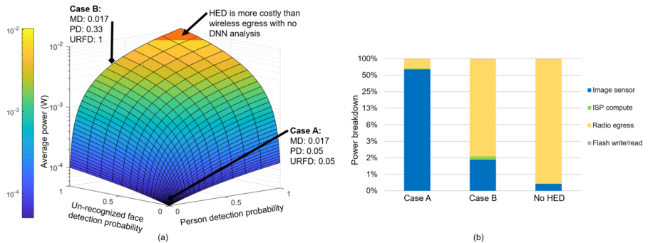
Fig. 6a shows the average system power for the above scenario, when the image sensor’s motion detection event rate is fixed to once per minute while the person detection (PD) and the un-registered face detection (URFD) event probabilities are varied. The URFD rate combines both face detection and face recognition, and it is assumed that data written to flash and sent wirelessly is uncompressed. This analysis motivates the use of HED for the chosen application, whereas the red top corner demarcates the PD and URFD probabilities where performing HED yields no power savings. In all other scenarios, HED enables significant (up to ) power reduction especially when both URFD and PD rates are low. Fig. 6b shows the system power breakdown for 3 event cases. When the total event rate is low (‘Case A’), the system power is dominated by the image sensor, while the wireless power dominates as the event rate increases. Notably, the ISP computation power for DNNs is always insignificant compared to the image sensor or radio, showing the benefit of HED in reducing overall power.
5. Data Compression Techniques
The proposed mm-scale imaging system has limited IC area for flash memory and on-chip SRAM, making it critical to employ aggressive data compression techniques for DNN parameters and images.
5.1. DNN parameter compression
High compression of up to 1.5bit/weight is achieved for DNNs by combining weight pruning, non-uniform quantization, Huffman encoding of quantized weights for convolutional layers, and index-based encoding for sparse fully-connected layers. The compressed sizes for person detection, face detection, and face recognition networks are 85kB, 112kB, and 107kB, respectively. Up to 1.75M compressed weights can be stored in the ISP NE on-chip SRAM, which are on-the-fly decompressed when moved to NE local SRAM buffers. Once weights are loaded into the SRAM buffers, they are heavily reused for convolution on large input activations so that the energy overhead of decompressing weights is negligible.
The proposed HED requires multiple DNNs but parameters for less frequently executed DNNs can be stored off-chip in flash to eliminate on-chip SRAM leakage power. This off-chip parameter loading approach, however, increases execution time and incurs energy overhead from inter-chip data movement. We first analyze the event frequency at which this on- vs. off-chip parameter storage trade-off is advantageous for each DNN, and then program each DNN based on the assumption of expected event frequency to minimize the average power consumption.
5.2. Image compression
We use a combination of several compression methods to minimize the data footprint and reduce wireless transmission cost.
5.2.1. JPEG and H.264 compression
The ISP performs on-the-fly JPEG compression on frames streamed in by the image sensor on a macro-block (MCB, 1616 pixel) level, reducing the memory footprint of storing images on-chip and the SRAM leakage power by 11 and only consuming 14.9J. As a result, both a reference and current frame can be stored on-chip in 180kB SRAM rather than off-chip, which otherwise would incur energy overheads of 407J/frame. We leverage the ISP’s customized H.264 intra-frame compression engine to reduce the memory footprint of a VGA frame by 23. We only apply H.264 to the image containing an unregistered face instead of all incoming VGA frames due to the higher latency (than JPEG) that cannot meet the image sensor interface throughput for on-the-fly compression. Though H.264 compression incurs 138% more processing energy than JPEG, at a system-level it reduces the flash write energy from 36.9J to 17.4J and the wireless egress energy from 37.7mJ to 17.8mJ as it attains a higher compression rate.
5.2.2. Change detection engine
Change detection between a new frame and reference frame stored on-chip can be performed on-the-fly by the ISP. Each MCB of an input frame is encoded into a 64b pattern vector and compared to the stored image vector to create a 4030 change detection map representing a non-rectangular RoI. We use a customized H.264 algorithm, which removes MCB inter-dependence, to compress only the non-rectangular RoI while unchanged MCBs are pruned. This achieves 135 compression compared to a VGA frame while consuming only 2.8J (assuming 86% scene pruning observed in our test dataset). At a system-level, combining change detection and H.264 compression reduces the flash write energy from 17.4J to 3J, the wireless egress energy from 17.8mJ to 3.1mJ, and allows for 74 images to be stored in flash.
5.2.3. Off-system image reconstruction
To reduce the wireless data egress, we reconstruct the current frame offline by only sending the change detection map (1.2kb) and the H.264 compressed RoI of the current frame (20-30kb) to a custom gateway. We assume that the imager system is deployed in a stationary location, so the system and gateway share the same reference image, which is periodically reprogrammed. A scene is reconstructed by decompressing the unchanged MCBs from the reference image and the changed MCBs from the current frame, reducing the egress data by 130.
6. Image correction for mm-scale Lens and ULP Front-Ends
Most cameras have 60∘ field of view (FOV), much less than a human. To achieve a larger FOV and capture more information for wide-view scene analysis, our system adopts a wide-angle lens. However, using this lens and a ULP image sensor that lacks sophisticated image pre-processing results in geometric and color distortion, negatively affecting the performance of deep learning perceptual tasks, as was demonstrated when deploying our system.
We propose image-correcting layers (ICL) that can be executed on the ISP NE using supported instructions, such as matrix multiplication and convolution, to compensate for artefacts and distortions (Fig. 7). Since ICL is based on DNN-compatible instructions, it does not require a dedicated hardware accelerator and can be generalized for other constrained systems.
6.1. Distortion modeling and compensation
The fisheye-like lens distortion is modeled by capturing checkerboard images using our system. Geometric distortion correction can be expressed by a mapping between pixels in the distorted image and the pixels in the correct image : . Various geometric distortion correction algorithms have been extensively studied and implemented (Ahlen et al., 2003)(T.Toutin, 2004). However, for real-time processing, a majority of them require task-specific hardware accelerators which are not available on our system.
| SCHEME | NETWORK SPARSITY | AVG. IOU | AVG. RECALL |
|---|---|---|---|
| 1 | 0% | 0.7570 | 0.9260 |
| 2 | 0% | 0.5769 | 0.7213 |
| 3 | 0% | 0.6648 | 0.7885 |
| 4 | 0% | 0.7453 | 0.8947 |
| 5 | 50% | 0.7172 | 0.8449 |
| 6 | 50% | 0.6254 | 0.7647 |
Instead, we construct a flow field matrix (FFM) that represents vertical and horizontal pixel-displacement vectors based on the offline constructed fisheye distortion model. This ICL can be performed by either the ISP Cortex-M0 or NE by representing the FFM as a sparse fully connected layer. This is advantageous compared to both conventional and learning-based distortion correction methods since it only requires a relatively small correction matrix, which has low memory and computational complexity.
Color correction is performed using a color correction matrix (CCM) that projects the RGB pixel values in the distorted image to the target RGB values at the same location in the corrected image, expressed by a linear equation for pixel where denotes the CCM. Our CCM is obtained by capturing images of an eSFR (edge spatial frequency response) chart using the proposed system. The color restoration ICL is implicitly accomplished with a linear layer in the custom face detection network. Training data images are modified using the color distortion matrix to emulate the system and implicitly learn the CCM.
METHOD SIZE PROCESSING ENERGY FLASH WRITE ENERGY EGRESS ENERGY EGRESS TIME VGA CAPACITY Raw VGA Image 3.7Mb 0 407J 414mJ 2 hours 0 JPEG 335kb 11.9J 36.9J 37.7mJ 11.6 min 1 H.264 (QF=20) 158.2kb 28.3J 17.4J 17.8mJ 5.5 min 12 H.264 + CD (QF=20) 27.4kb 14.8J 3J 3.1mJ 57s 74
6.2. Experiments on ICLs for Face Detection
The proposed ICLs were tested using images in the COCO-faces dataset, a dataset with annotated human faces sourced from COCO 2017 (Lin et al., 2014), and on images captured by our system. We first pre-train the customized YOLO-Lite network without distortion to speed up convergence, then apply the distortion models to the training/validation dataset, and include the pre-determined geometric distortion correction ICL. Finally, we fine-tune the YOLO model for color correction.
The performance of our proposed YOLO-Lite face detection network with ICLs is quantified by evaluating the average intersection over union (IoU) and average recall. In Table 1, we evaluate six schemes: 1) original images, 2) images with modeled imager geometric and color distortions, 3) geometric distortion correction, 4) additionally fine-tuning the face detection network using the color distorted training dataset, 5) additionally applying 50% network pruning, 8-bit fixed point quantization, and parameter compression to the final network (necessary for on-chip parameter storage), and 6) testing scheme 5 on a 112112 pixel gray-scale input image.
The results show a substantial performance drop after applying the modeled distortion to the original image data. Both performance measures are improved to a level close to the original when lens distortion and color restoration ICLs are applied. We experimented on the impact of using a smaller input gray-scale image, together with down-graded intermediate feature maps (case 6 in Table 1). The results demonstrate that our proposed image correction and face detection pipeline give sensible performance in this case, showing that it can be extended to other highly-constrained systems.
7. Integrated System Evaluation
We have integrated a mm-scale, standalone intelligent imaging system (Fig.1) for an intruder detection demonstration while employing the methods discussed in Sections 2,4-6. Table 2 outlines the gains of each compression method relative to a raw VGA image, which yield proportional energy savings when writing the image data to flash and transmitting the data via the ULP wireless transmitter. Using the combination of H.264 and change detection-based compression significantly decreases the egress energy to 3.1mJ and the egress time to 5 minutes, making the system more practical for a real-life scenario. This final method extends the lifetime when performing continuous motion-detection, VGA capture, flash storage and wireless egress by 13 without battery recharging.
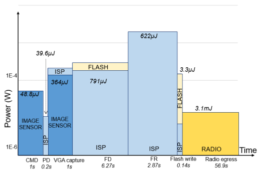
Fig. 8 shows the intruder detection scenario flow using HED, including the energy consumption and execution time of each system behavior. The ISP runs at a relative low clock frequency of 240kHz (programmable) to maintain low power. This processing performance (latency of each step in Fig. 8) is acceptable for our target scenario where the event of interest is infrequently triggered. Fig. 4 shows examples of actual images processed by the system through the proposed multi-DNN and image compression data path.
The radio’s link distance and data rate can be adjusted by modifying the number of repeated pulses, the pulse width and separation, and the decap recharging time. Two different modes were selected and measured in a line-of-sight indoor environment. The long distance mode achieves a link distance of 20m, a data rate of 256bps, and an egress time for a compressed image of 106s. The short distance mode has a shorter distance of 15m, but it achieves a higher data rate of 480bps and shorter transmit time of 56s.
For system lifetime analysis, we assume that a motion-triggered sub-sampled frame is sent to the ISP every 20 minutes to perform person detection. When HED is used (assuming event ratios of 1:2, 1:2 and 1:5 for PD, FD and FR), the overall average power consumption is 49.6W for an expected battery lifetime of 7 days, which can be extended by trading off larger system size for a higher capacity battery. The total power consumption of the system when the ISP layer is not retaining any image or DNN data is 7.35W, giving a total shelf-life of 48 days without recharging. In this (re)charging mode, the harvester and solar layers can provide 10W to recharge the battery under 10klux lighting conditions to extend the total shelf-life until system (re)deployment.
8. Conclusion
This paper proposes a novel mm-scale, standalone system with deep-learning and image processing for intruder detection, with an average power consumption of 49.6W and expected lifetime of 7 days without recharging. It achieves a miniature size by vertically stacking ULP custom ICs, and satisfies a tight memory and energy budget through a combination of data/energy management methods. We present image-enhancement layers to improve DNN performance in constrained embedded systems. Comprehensive system-level analysis was conducted to quantify the gain of proposed techniques, which can be generalized to other ULP systems. Having demonstrated a tiny-IoT intelligent imaging system, analysis through a sociotechnical and ethical lens is an essential next step; we invite future work on topics such as security and privacy.
Acknowledgements.
The authors would like to thank Sony Semiconductor Solutions Corp./Sony electronics Inc. for supporting this work.References
- (1)
- Ahlen et al. (2003) T. Ahlen, H. Broszio, and I. Wassermann. 2003. Robust Line-Based Calibration of Lens Distortion from a Single View. Mirage 2003 (05 2003).
- Ajani et al. (2021) T. S. Ajani, A. L. Imoize, and A. A. Atayero. 2021. An Overview of Machine Learning within Embedded and Mobile Devices–Optimizations and Applications. Sensors 21, 13 (2021). https://doi.org/10.3390/s21134412
- An et al. (2020) H. An, S. Venkatesan, S. Schiferl, T. Wesley, Q. Zhang, J. Wang, K. Choo, S. Liu, B. Liu, Z. Li, H. Zhong, L. Gong, D. Blaauw, R. Dreslinski, D. Sylvester, and H. S. Kim. 2020. A 170W Image Signal Processor Enabling Hierarchical Image Recognition for Intelligence at the Edge. In 2020 IEEE Symposium on VLSI Circuits. 1–2.
- Balasubramanian et al. (2018) S. Balasubramanian, Y. M. Chukewad, J. M. James, G. L. Barrows, and S. B. Fuller. 2018. An Insect-Sized Robot That Uses a Custom-Built Onboard Camera and a Neural Network to Classify and Respond to Visual Input. In 2018 7th IEEE International Conference on Biomedical Robotics and Biomechatronics (Biorob). 1297–1302. https://doi.org/10.1109/BIOROB.2018.8488007
- Bick et al. (2021) C.S. Bick, I. Lee, T. Coote, A.E. Haponski, and D. Blaauw. 2021. Millimeter-sized smart sensors reveal that a solar refuge protects tree snail Partula hyalina from extirpation. In Commun Biol, Vol. 4. https://doi.org/10.1038/s42003-021-02124-y
- Chen et al. (2016) Y. Chen, N. Chiotellis, L. Chuo, C. Pfeiffer, Y. Shi, R. G. Dreslinski, A. Grbic, T. Mudge, D. D. Wentzloff, D. Blaauw, and H. Kim. 2016. Energy-Autonomous Wireless Communication for Millimeter-Scale Internet-of-Things Sensor Nodes. IEEE Journal on Selected Areas in Communications 34, 12 (2016), 3962–3977. https://doi.org/10.1109/JSAC.2016.2612041
- Choo et al. (2019) K. D. Choo, L. Xu, Y. Kim, J. Seol, X. Wu, D. Sylvester, and D. Blaauw. 2019. Energy-Efficient Motion-Triggered IoT CMOS Image Sensor With Capacitor Array-Assisted Charge-Injection SAR ADC. IEEE Journal of Solid-State Circuits 54, 11 (2019), 2921–2931.
- Dong et al. (2017) Q. Dong, Y. Kim, I. Lee, M. Choi, Z. Li, J. Wang, K. Yang, Chen. Y., J. Dong, M. Cho, G. Kim, W. Chang, Y. Chen, Y. Chih, D. Blaauw, and D. Sylvester. 2017. 11.2 A 1Mb embedded NOR flash memory with 39W program power for mm-scale high-temperature sensor nodes. In 2017 IEEE International Solid-State Circuits Conference (ISSCC). 198–199.
- Huang et al. (2018) R. Huang, J. Pedoeem, and C. Chen. 2018. YOLO-LITE: A Real-Time Object Detection Algorithm Optimized for Non-GPU Computers. In 2018 IEEE International Conference on Big Data (Big Data). 2503–2510. https://doi.org/10.1109/BigData.2018.8621865
- Iyer et al. (2020) V. Iyer, Ali. Najafi, J. James, S. Fuller, and S. Gollakota. 2020. Wireless steerable vision for live insects and insect-scale robots. In Science Robotics, Vol. 5. https://doi.org/10.1126/scirobotics.abb0839
- Ji et al. (2016) Suyao Ji, Jing Pu, Byong Chan Lim, and Mark Horowitz. 2016. A 220pJ/pixel/frame CMOS image sensor with partial settling readout architecture. In 2016 IEEE Symposium on VLSI Circuits (VLSI-Circuits). 1–2. https://doi.org/10.1109/VLSIC.2016.7573545
- Jia et al. (2021) H. Jia, M. Ozatay, Y. Tang, H. Valavi, R. Pathak, J. Lee, and N. Verma. 2021. 15.1 A Programmable Neural-Network Inference Accelerator Based on Scalable In-Memory Computing. In 2021 IEEE International Solid- State Circuits Conference (ISSCC), Vol. 64. 236–238. https://doi.org/10.1109/ISSCC42613.2021.9365788
- Josephson et al. (2019) C. Josephson, L. Yang, P. Zhang, and S. Katti. 2019. Wireless Computer Vision Using Commodity Radios. In Proceedings of the 18th International Conference on Information Processing in Sensor Networks (Montreal, Quebec, Canada) (IPSN ’19). Association for Computing Machinery, New York, NY, USA, 229–240. https://doi.org/10.1145/3302506.3310403
- Jung et al. (2016) W. Jung, J. Gu, P. D. Myers, M. Shim, S. Jeong, K. Yang, M. Choi, Z. Foo, S. Bang, S. Oh, D. Sylvester, and D. Blaauw. 2016. 8.5 A 60%-efficiency 20nW-500µW tri-output fully integrated power management unit with environmental adaptation and load-proportional biasing for IoT systems. In 2016 IEEE International Solid-State Circuits Conference (ISSCC). 154–155. https://doi.org/10.1109/ISSCC.2016.7417953
- Jung et al. (2014) W. Jung, S. Oh, S. Bang, Y. Lee, Z. Foo, G. Kim, Y. Zhang, D. Sylvester, and D. Blaauw. 2014. An Ultra-Low Power Fully Integrated Energy Harvester Based on Self-Oscillating Switched-Capacitor Voltage Doubler. IEEE Journal of Solid-State Circuits 49, 12 (2014), 2800–2811. https://doi.org/10.1109/JSSC.2014.2346788
- Kim et al. (2014) G. Kim, Y. Lee, Zhiyoong Foo, P. Pannuto, Ye-Sheng Kuo, B. Kempke, M. H. Ghaed, Suyoung Bang, Inhee Lee, Yejoong Kim, Seokhyeon Jeong, P. Dutta, D. Sylvester, and D. Blaauw. 2014. A millimeter-scale wireless imaging system with continuous motion detection and energy harvesting. In 2014 Symposium on VLSI Circuits Digest of Technical Papers. 1–2. https://doi.org/10.1109/VLSIC.2014.6858425
- Lee et al. (2019) J. Lee, E. Mok, J. Huang, L. Cui, A. Lee, V. Leung, P. Mercier, S. Shellhammer, L. Larson, P. Asbeck, R. Rao, Y. Song, A. Nurmikko, and F. Laiwalla. 2019. An Implantable Wireless Network of Distributed Microscale Sensors for Neural Applications. In 2019 9th International IEEE/EMBS Conference on Neural Engineering (NER). 871–874. https://doi.org/10.1109/NER.2019.8717023
- Lefebvre et al. (2021) M. Lefebvre, L. Moreau, R. Dekimpe, and D. Bol. 2021. 7.7 A 0.2-to-3.6TOPS/W Programmable Convolutional Imager SoC with In-Sensor Current-Domain Ternary-Weighted MAC Operations for Feature Extraction and Region-of-Interest Detection. In 2021 IEEE International Solid- State Circuits Conference (ISSCC), Vol. 64. 118–120. https://doi.org/10.1109/ISSCC42613.2021.9365839
- Lin et al. (2014) T. Lin, M Maire, S. Belongie, J. Hays, P. Perona, D. Ramanan, P. Dollár, and C. L. Zitnick. 2014. Microsoft COCO: Common Objects in Context. In European Conference on Computer Vision (ECCV) (2014-01-01). Zürich. cocodataset.org Oral.
- Lu et al. (2021) Y. Lu, V. L. Le, and T. T. Kim. 2021. 9.7 A 184 µ W Real-Time Hand-Gesture Recognition System with Hybrid Tiny Classifiers for Smart Wearable Devices. In 2021 IEEE International Solid- State Circuits Conference (ISSCC), Vol. 64. 156–158. https://doi.org/10.1109/ISSCC42613.2021.9365963
- Moon et al. (2019) E. Moon, I. Lee, D. Blaauw, and J.D. Phillips. 2019. High-efficiency photovoltaic modules on a chip for millimeter-scale energy harvesting. Progress in Photovoltaics: Research and Applications 27, 6 (2019), 540–546. https://doi.org/10.1002/pip.3132
- Morishita et al. (2021) F. Morishita, N. Kato, S. Okubo, T. Toi, M. Hiraki, S. Otani, H. Abe, Y. Shinohara, and H. Kondo. 2021. A CMOS Image Sensor and an AI Accelerator for Realizing Edge-Computing-Based Surveillance Camera Systems. In 2021 Symposium on VLSI Circuits. 1–2. https://doi.org/10.23919/VLSICircuits52068.2021.9492514
- Naderiparizi et al. (2017) S. Naderiparizi, P. Zhang, M. Philipose, B. Priyantha, J. Liu, and D. Ganesan. 2017. Glimpse: A Programmable Early-Discard Camera Architecture for Continuous Mobile Vision. In Proceedings of the 15th Annual International Conference on Mobile Systems, Applications, and Services (Niagara Falls, New York, USA) (MobiSys ’17). Association for Computing Machinery, New York, NY, USA, 292–305. https://doi.org/10.1145/3081333.3081347
- Pannuto et al. (2015) P. Pannuto, Y. Lee, Y. Kuo, Z. Foo, B. Kempke, G. Kim, R. G. Dreslinski, D. Blaauw, and P. Dutta. 2015. MBus: An ultra-low power interconnect bus for next generation nanopower systems. In 2015 ACM/IEEE 42nd Annual International Symposium on Computer Architecture (ISCA). 629–641.
- Rossi et al. (2021) D. Rossi, F. Conti, M. Eggiman, S. Mach, A. D. Mauro, M. Guermandi, G. Tagliavini, A. Pullini, I. Loi, J. Chen, E. Flamand, and L. Benini. 2021. 4.4 A 1.3TOPS/W @ 32GOPS Fully Integrated 10-Core SoC for IoT End-Nodes with 1.7W Cognitive Wake-Up From MRAM-Based State-Retentive Sleep Mode. In 2021 IEEE International Solid- State Circuits Conference (ISSCC), Vol. 64. 60–62. https://doi.org/10.1109/ISSCC42613.2021.9365939
- Smets et al. (2019) S. Smets, T. Goedemé, A. Mittal, and M. Verhelst. 2019. 2.2 A 978GOPS/W Flexible Streaming Processor for Real-Time Image Processing Applications in 22nm FDSOI. In 2019 IEEE International Solid- State Circuits Conference - (ISSCC). 44–46. https://doi.org/10.1109/ISSCC.2019.8662346
- Song et al. (2020) M. Song, M. Ding, E. Tiurin, K. Xu, E. Allebes, G. Singh, P. Zhang, S. Traferro, H. Korpela, N. Van Helleputte, R. B. Staszewski, Y. Liu, and C. Bachmann. 2020. 30.8 A 3.5mm×3.8mm Crystal-Less MICS Transceiver Featuring Coverages of ±160ppm Carrier Frequency Offset and 4.8-VSWR Antenna Impedance for Insertable Smart Pills. In 2020 IEEE International Solid- State Circuits Conference - (ISSCC). 474–476. https://doi.org/10.1109/ISSCC19947.2020.9063083
- Thijssen et al. (2020) B. J. Thijssen, E. A. M. Klumperink, P. Quinlan, and B. Nauta. 2020. 30.4 A 370µW 5.5dB-NF BLE/BT5.0/IEEE 802.15.4-Compliant Receiver with gt;63dB Adjacent Channel Rejection at gt;2 Channels Offset in 22nm FDSOI. In 2020 IEEE International Solid- State Circuits Conference - (ISSCC). 466–468. https://doi.org/10.1109/ISSCC19947.2020.9062973
- T.Toutin (2004) T.Toutin. 2004. Review article: Geometric processing of remote sensing images: models, algorithms and methods. International Journal of Remote Sensing 25, 10 (2004), 1893–1924. https://doi.org/10.1080/0143116031000101611
- Xu et al. (2021) H. Xu, Z. Li, N. Lin, Q. Wei, F. Qiao, X. Yin, and H. Yang. 2021. MACSen: A Processing-In-Sensor Architecture Integrating MAC Operations Into Image Sensor for Ultra-Low-Power BNN-Based Intelligent Visual Perception. IEEE Transactions on Circuits and Systems II: Express Briefs 68, 2 (2021), 627–631. https://doi.org/10.1109/TCSII.2020.3015902