Lasing in the Space Charge-Limited Current Regime
Abstract
We introduce an analytical model for ideal organic laser diodes based on the argument that their intrinsic active layers necessitate operation in the bipolar space charge-limited current regime. Expressions for the threshold current and voltage agree well with drift-diffusion modeling of complete p-i-n devices and an analytical bound is established for laser operation in the presence of annihilation and excited-state absorption losses. These results establish a foundation for the development of organic laser diode technology.
Epitaxial inorganic semiconductors are the basis for nearly all laser diodes today. Organic semiconductors could provide a new, wavelength-tunable laser diode platform, but are disadvantaged by lower charge carrier mobility, lower thermal conductivity, and more efficient excited state quenching interactions. Beyond their material properties, however, organic and inorganic laser diodes also fundamentally differ in their mode of electrical operation: gain in the inorganic case is driven by diffusion current in a p-n junction,Coldren et al. (2012), whereas in the organic case, the need for an intrinsic active layer (since electrical doping severely quenches organic semiconductor excited statesForrest (2020); Köhler and Bässler (2015)) requires gain to be achieved by a space charge-limited (SCL) drift current. Although the impact of SCL current is well-appreciated for organic light emitting diodes (OLEDs)Forrest (2020), its implications for organic laser diode operation have not been explored in detail.
Here, we derive expressions for the threshold voltage and current density of ideal organic laser diodes where gain is provided by a bipolar SCL current in the intrinsic active layer of a p-i-n device. The results are extended to treat organic laser operation in the presence of triplet exciton and polaron losses, and are validated using the commercial device simulator Setfosnoa (2020). As organic laser efforts accelerate following the initial demonstration by Sandanayaka et al. (2019), the framework established here should prove useful for guiding future development.
Space charge effects become significant in a semiconductor when the transit time of electrons and holes drifting across it (, where is the layer thickness, is the applied voltage, is the built in potential, and is the electron or hole mobility) is smaller than the dielectric relaxation time, , set by its dielectric constant () and equilibrium free charge density (, , with representing the elementary charge). In essence, this situation corresponds to injecting more charge into the semiconductor than exists in equilibrium and it is frequently the case in undoped organic semiconductorsForrest (2020); Köhler and Bässler (2015); Pope et al. (1999). Organic laser diodes are generally expected to operate in this regime because 1) they operate at high current density where drift dominates diffusion and 2) although their electron and hole transport layers are typically doped to achieve high conductivitySandanayaka et al. (2019), their active layer (i.e. gain region) must remain intrinsic to avoid strong exciton quenching with ionized dopant and polaron species. Thus, is well-satisfied and, notwithstanding the limited diffusion of charge carriers from the contacts/transport layers into the active layerWetzelaer and Blom (2014), optical gain must be achieved in the bipolar SCL current regime.
The two-carrier SCL current problem was originally solved by Parmenter and Ruppel for the ideal case of a trap-free insulatorParmenter and Ruppel (1959). The result exhibits the same dependence as the unipolar case, but predicts an enhancement of the overall current density that depends on the recombination rate between electrons and holes. In the following, we use this solution to establish analytical bounds and scaling relationships for an ideal organic laser diode with Ohmic electron and hole injection into the active layer; any limitations on injection would constitute a source of non-ideality.
In organic semiconductors with a large exciton binding energy and exchange splitting between bright (singlet) and dark (triplet) exciton states, the net modal gain can be expressed as:
| (1) |
where is the modal confinement factor, is the stimulated emission cross-section, is the singlet exciton density, is the transparency density, and is the net optical loss due to outcoupling, scattering, or parasitic absorption from other materials or excited states. At threshold, and thus the threshold singlet density is:
| (2) |
The singlet density is governed by the rate equation:
| (3) |
where is the exciton generation rate due to Langevin recombination of electrons and holes (i.e. , where )Pope et al. (1999), is the singlet spin fractionSegal et al. (2003), is the natural singlet decay rate, and accounts for any additional quenching processes such as exciton-exciton and exciton-polaron annihilation explored below. The term on the right-hand side of Eq. (3) accounts for stimulated emission, with and equal to the photon density and group velocity of the lasing mode, respectively.
At threshold, and thus Eq. (3) can be solved in steady state to yield the threshold recombination rate:
| (4) |
which factors into an ideal rate multiplied by exciton and optical loss terms in parentheses. Equation (4) is derived assuming a spatially uniform exciton density, which is rigorously valid for the ideal case of as shown below, and thus also justifies the neglect of exciton diffusion in Eq. (3).
The Parmenter-Ruppel solution subsequently establishes the link between recombination rate, voltage, and current density in the device. The general result is provided in the Supplementary Material; however, we focus here on the specific case of equal electron and hole mobilities () and perfect charge balance (i.e. every injected electron recombines with a hole in the active layer) since it constitutes the limit of an ideal organic laser diode.
The current-voltage relationship is given by the Mott-Gurney law:
| (5) |
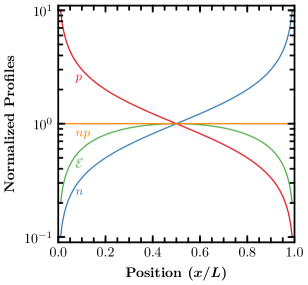
but with an effective mobility, , larger than that of the individual carriers due to the neutralization of space charge by recombination. For the assumed case of Ohmic electron and hole injection into the active layer, the built-in potential is approximated by the bandgap energy, . The position, electric field, and carrier densities are most conveniently expressed parametrically in terms of the fractional electron current :
| (6a) | ||||||
| (6b) | ||||||
Each quantity scales linearly with the applied voltage (square root of the current) and is shown normalized to its value at the midpoint of the active layer in Fig. 1. The product is spatially uniform as evident from inspection of Eq. (6b), justifying the neglect of spatial variation in deriving Eq. (4). As in the case of unipolar SCL current, these equations break down in the immediate vicinity of the contacts as the field drops to zero and transport becomes diffusive.
It is subsequently straightforward to evaluate the current density and voltage in terms of the recombination rate at threshold:
| (7) |
The expression for follows directly from particle conservation due to the assumption of perfect charge balance and shows that the simple dimensional analysis estimate commonly used in the literatureKozlov et al. (2000) is exact for a bipolar SCL current. We note that, although Eq. (7) is derived under the assumption , it remains reasonably accurate even when the mobilities differ by up to an order of magnitude provided that their average value is used for ; see the Supplementary Material for details.
In evaluating from Eq. (4), we note that, while can be obtained from thermodynamic considerations (see the Supplementary Material), it is immaterial in practice because the cold cavity loss () typically satisfies and thus , which is readily determined from the threshold singlet density () measured experimentally under impulsive optical pump conditions. Taking parameter values typical of the 4,4′-bis[(N-carbazole)styryl]bi-phenyl (BSBCz) diode lasers reported by Sandanayaka et al. (2019): cm-3, ns-1, , cmVs-1, eV, and nm, we obtain A cm-2, V and a threshold power density kW cm-2 as lower bounds for laser operation. For comparison, the experimentally-recorded values are A cm-2, V and kW cm-2Sandanayaka et al. (2019).
Equation (7) highlights the importance of active layer thickness for organic laser diodes. Whereas depends weakly on since to first order, the threshold voltage and power density both scale as . The is important in the context of thermal management because organic laser diodes not only generate more heat than their inorganic counterparts (due to their higher voltage), but have more difficulty dissipating it (due to their lower thermal conductivity) and are less able to withstand high temperature without degrading. Electric field strength, which scales as , is another concern since its maximum in the example above ( MV cm-1) is comparable to the MV cm-1 breakdown field of many organic semiconductorsForrest (2020); Köhler and Bässler (2015); Pope et al. (1999). To this point, dielectric breakdown was reported after roughly fifty pulses near threshold in Ref. Sandanayaka et al. (2019).
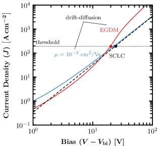
Given that the threshold relations above neglect the existence of charge transport layers and also assume infinite carrier densities at the active layer interfaces, it is important to test the accuracy of these results against full drift-diffusion modeling of a real device architecture. Retaining the BSBCz parameters from above, we treat the case of an organic laser with a 150 nm-thick intrinsic active layer and fix the majority carrier concentrations at each edge to cm-3 to simulate Ohmic injection from heavily doped transport layers. Drift-diffusion simulations are carried out using the commercial software Setfosnoa (2020) and the results are presented in Fig. 2 for the case of a constant mobility ( cmVs-1; blue) and for the case in which it depends locally on electric field and carrier density according to the extended Gaussian disorder model (EGDM, red); details of the EGDM are provided in the Supplementary Material. The threshold current density in both simulations is in good agreement with the analytical prediction; however, the threshold voltage in the EGDM case is slightly lower. This is due to the increase in mobility with field and carrier concentration in the EGDM model, which highlights the importance of using mobility values that are congruent with the conditions at threshold.
From Fig. 1, it is evident that to sustain the electron and hole concentrations in the middle of the device (and thus the product everywhere), the majority carrier concentrations injected at the active layer edges must be roughly an order of magnitude higher. Inserting A cm-2 from Fig. 2 into Eq. (6b) suggests that edge carrier concentrations as low as cm-3 are sufficient to maintain charge balance up to the lasing threshold, in agreement with the full drift-diffusion model. This is important because it sets the minimum doping concentration required for the transport layers in a laser diode (i.e. due to continuity of and ) which, notably, is within the range typical for p-i-n OLEDs Walzer et al. (2007); more detail on this point is provided in the Supplementary Material.
At this stage, it is also important to assess the impact of triplet exciton and polaron-related optical losses (due to respective absorption cross-sections Zhang and Forrest (2011) and at the lasing wavelength) and quenching interactions (with respective annihilation rate coefficients and ) Baldo et al. (2002); Gärtner et al. (2007). Because the latter typically depend on the former through Förster energy transferYokota and Tanimoto (1967), absorption and annihilation losses must be treated on equal footing. Assuming only one species of polaron (holes in this case) is detrimental, the quenching rate in Eq. (3) becomes and the loss in Eq. (1) becomes , where is the hole density at the midpoint of the active layer. Using the threshold singlet density in the absence of triplet and polaron losses, (defined in Eq. (2) by the cold cavity loss), Eq. (4) can be rewritten in the form of an implicit quartic equation:
| (8) |
In this expression, the rise time () is important because it determines the extent to which long-lived triplet excitons accumulate before the full current density is achieved (i.e. by the time the full recombination rate, , is reached)Giebink and Forrest (2009). Although is nominally characteristic of the electrical pulse, it cannot be significantly faster than the transit time of charge carriers drifting across the active layer since this is the time it takes to establish the SCL recombination profile to begin with ( ns for the BSBCz example above) Many and Rakavy (1962). Note also that, in seeking to approximate the spatially nonuniform polaron density with a single effective value for annihilation and absorption, it is more accurate to use the midpoint density for the former and the layer-averaged density () for the latter as discussed in the Supplementary Material.
The form of Eq. (8) is useful because it allows the impact of each loss mechanism to be understood individually. For example, singlet-triplet annihilation on its own doubles the threshold when the middle term in the first set of parentheses is equal to unity, which corresponds to the situation where . More generally, for Eq. (8) to have any physically meaningful solution, the absorption and annihilation coefficients must satisfy the following inequalities:
| (9a) | |||
| (9b) | |||
Figures 3(a) and 3(b) plot these bounds for triplet and polaron losses, respectively, along with contours that show the relative increase in threshold caused by each species. Figure 3(b) also includes the results from full Setfos numerical modeling (solid symbols) of the polaron case, validating the midpoint and average carrier density approximations used to derive Eq. (8).
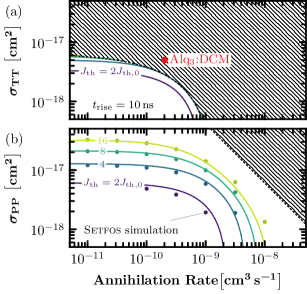
These results highlight the difference between triplet losses, where a small increase in absorption cross-section or annihilation coefficient can mean the difference between a modest threshold increase and prevention of lasing outright, and polaron losses, where the penalty is more gradual and does not depend on external factors like or . A blunt way of characterizing this difference is that triplet excitons are either insignificant or catastrophic, whereas the region of parameter space between these extremes is broader for polarons. This highlights the importance of designing new organic gain media like BSBCz that have low overlap between their emission and triplet-triplet absorption spectra Sandanayaka et al. (2019), and of implementing device architectures that can deliver high-speed electrical pulsesChime et al. (2018), since this is the difference between success and failure for the classic Alq3:DCMGiebink and Forrest (2009) gain medium in Fig. 3(a).
Another intuitive, but important guideline is to seek organic gain media with equal (and maximal) electron and hole mobilities. To the extent that perfect charge balance is maintained and the envelope of the lasing mode varies negligibly over the active layer, the general solution for given in the Supplementary Material shows that Eq. (7) is largely unaffected when the mobility of one carrier dominates (in this case is just the mobility of the more mobile charge carrier). The problem with imbalanced mobility, however, is that it concentrates recombination toward the lower mobility carrier side of the active layer. This not only exacerbates annihilation loss, but also makes it more challenging to maintain charge balance since the less mobile carrier must be injected at higher density to sustain the same total recombination rate in a narrower region of space; full details are provided in the Supplementary Material.
Finally, we note that the framework developed here may also be relevant for metal halide perovskite (MHP) lasers. Though SCL current is less well-studied in this material class (due in part to complications with ion movement)Duijnstee et al. (2020); Sajedi Alvar et al. (2020), the observation that MHP light emitting diodes use undoped active layersGunnarsson and Rand (2020); Liu et al. (2020) along with the fact that electrical doping is a basic challenge for these materials to begin withDuijnstee et al. (2020) makes it plausible that a future MHP laser diode will operate in the bipolar SCL current regime. In this case, however, recombination tends to be sub-Langevin (i.e. the bimolecular recombination coefficient is substantially smaller than the Langevin rate), which causes bipolar SCL current to take place in the injected plasma regime where everywhereLampert and Rose (1961). Unfortunately, the analytical solution in this limit can greatly overestimate the threshold current because diffusion strongly modifies the product (and thus the recombination current) near the active layer edges (see the Supplementary Material for an example). A full drift-diffusion model is therefore required to accurately describe MHP lasers.
In conclusion, we have put forth a model for organic laser diodes that operate in the bipolar space charge-limited current regime. We have obtained analytical expressions for the threshold voltage and current density and have identified fundamental limits for laser operation in the presence of parasitic annihilation and excited state absorption losses. These results, together with the experiments of Sandanayaka et al. (2019), emphasize a shift in strategy from OLED-like architectures characterized by many heterojunctions, blocking layers, and so forth, to a p-i-n structure based on a single, low threshold material that can be degenerately p- and n-doped, and that has no triplet or polaron absorption overlapping with its emission. With rational design of organic laser materials now emerging to meet these criteria Ou et al. (2020) and the model here to predict device performance, the future of organic laser diode technology is coming into clearer focus.
Acknowledgements.
This work was supported in part by AFOSR Award no. FA9550-18-1-0037 and DARPA Award no N66001-20-1-4052.References
- Coldren et al. (2012) L. A. Coldren, S. W. Corzine, and M. L. Mashanovitch, Diode lasers and photonic integrated circuits, 2nd ed., Wiley series in microwave and optical engineering No. 218 (Wiley, Hoboken, N.J, 2012).
- Forrest (2020) S. Forrest, Organic electronics: foundations to applications (Oxford University Press, New York, 2020).
- Köhler and Bässler (2015) A. Köhler and H. Bässler, Electronic processes in organic semiconductors: an introduction (Wiley-VCH, Weinheim, 2015).
- noa (2020) Setfos, v 5.1 (FLUXiM AG, 2020).
- Sandanayaka et al. (2019) A. S. D. Sandanayaka, T. Matsushima, F. Bencheikh, S. Terakawa, W. J. Potscavage, C. Qin, T. Fujihara, K. Goushi, J.-C. Ribierre, and C. Adachi, Indication of current-injection lasing from an organic semiconductor, Appl. Phys. Express 12, 061010 (2019).
- Pope et al. (1999) M. Pope, C. E. Swenberg, and M. Pope, Electronic processes in organic crystals and polymers, 2nd ed., Monographs on the physics and chemistry of materials No. 56 (Oxford University Press, New York, 1999).
- Wetzelaer and Blom (2014) G. A. H. Wetzelaer and P. W. M. Blom, Ohmic current in organic metal-insulator-metal diodes revisited, Phys. Rev. B 89, 241201(R) (2014).
- Parmenter and Ruppel (1959) R. H. Parmenter and W. Ruppel, Two-Carrier Space-Charge-Limited Current in a Trap-Free Insulator, J. Appl. Phys. 30, 1548 (1959).
- Segal et al. (2003) M. Segal, M. A. Baldo, R. J. Holmes, S. R. Forrest, and Z. G. Soos, Excitonic singlet-triplet ratios in molecular and polymeric organic materials, Phys. Rev. B 68, 075211 (2003).
- Kozlov et al. (2000) V. Kozlov, G. Parthasarathy, P. Burrows, V. Khalfin, J. Wang, S. Chou, and S. Forrest, Structures for organic diode lasers and optical properties of organic semiconductors under intense optical and electrical excitations, IEEE J. Quantum Electron. 36, 18 (2000).
- Walzer et al. (2007) K. Walzer, B. Maennig, M. Pfeiffer, and K. Leo, Highly Efficient Organic Devices Based on Electrically Doped Transport Layers, Chem. Rev. 107, 1233 (2007).
- Zhang and Forrest (2011) Y. Zhang and S. R. Forrest, Existence of continuous-wave threshold for organic semiconductor lasers, Phys. Rev. B 84, 241301(R) (2011).
- Baldo et al. (2002) M. A. Baldo, R. J. Holmes, and S. R. Forrest, Prospects for electrically pumped organic lasers, Phys. Rev. B 66, 035321 (2002).
- Gärtner et al. (2007) C. Gärtner, C. Karnutsch, U. Lemmer, and C. Pflumm, The influence of annihilation processes on the threshold current density of organic laser diodes, J. Appl. Phys. 101, 023107 (2007).
- Yokota and Tanimoto (1967) M. Yokota and O. Tanimoto, Effects of Diffusion on Energy Transfer by Resonance, J. Phys. Soc. Jpn. 22, 779 (1967).
- Giebink and Forrest (2009) N. C. Giebink and S. R. Forrest, Temporal response of optically pumped organic semiconductor lasers and its implication for reaching threshold under electrical excitation, Phys. Rev. B 79, 073302 (2009).
- Many and Rakavy (1962) A. Many and G. Rakavy, Theory of Transient Space-Charge-Limited Currents in Solids in the Presence of Trapping, Phys. Rev. 126, 1980 (1962).
- Nakanotani et al. (2007) H. Nakanotani, C. Adachi, S. Watanabe, and R. Katoh, Spectrally narrow emission from organic films under continuous-wave excitation, Appl. Phys. Lett. 90, 231109 (2007).
- Chime et al. (2018) A. C. Chime, S. Bensmida, M. Chakaroun, M. W. Lee, H. Nkwawo, and A. P. A. Fischer, Electrical modelling and design of ultra-fast micro-OLED with coplanar wave-guided electrodes in ON-OFF regime, Org. Electron. 56, 284 (2018).
- Duijnstee et al. (2020) E. A. Duijnstee, J. M. Ball, V. M. Le Corre, L. J. A. Koster, H. J. Snaith, and J. Lim, Toward Understanding Space-Charge Limited Current Measurements on Metal Halide Perovskites, ACS Energy Lett. 5, 376 (2020).
- Sajedi Alvar et al. (2020) M. Sajedi Alvar, P. W. M. Blom, and G.-J. A. H. Wetzelaer, Space-charge-limited electron and hole currents in hybrid organic-inorganic perovskites, Nat. Commun. 11, 4023 (2020).
- Gunnarsson and Rand (2020) W. B. Gunnarsson and B. P. Rand, Electrically driven lasing in metal halide perovskites: Challenges and outlook, APL Mater. 8, 030902 (2020).
- Liu et al. (2020) X.-K. Liu, W. Xu, S. Bai, Y. Jin, J. Wang, R. H. Friend, and F. Gao, Metal halide perovskites for light-emitting diodes, Nat. Mater. 10.1038/s41563-020-0784-7 (2020).
- Lampert and Rose (1961) M. A. Lampert and A. Rose, Volume-Controlled, Two-Carrier Currents in Solids: The Injected Plasma Case, Phys. Rev. 121, 26 (1961).
- Ou et al. (2020) Q. Ou, Q. Peng, and Z. Shuai, Computational screen-out strategy for electrically pumped organic laser materials, Nat. Commun. 11, 4485 (2020).