Current address: ]Beijing Academy of Quantum Information Sciences, 100193 Beijing, China
Large Second-Order Josephson Effect in Planar Superconductor-Semiconductor Junctions
Abstract
We investigate the current-phase relations of Al/InAs-quantum well planar Josephson junctions fabricated using nanowire shadowing technique. Based on several experiments, we conclude that the junctions exhibit an unusually large second-order Josephson harmonic, the term. First, superconducting quantum interference devices (dc-SQUIDs) show half-periodic oscillations, tunable by gate voltages as well as magnetic flux. Second, Josephson junction devices exhibit kinks near half-flux quantum in supercurrent diffraction patterns. Third, half-integer Shapiro steps are present in the junctions. Similar phenomena are observed in Sn/InAs quantum well devices. We perform data fitting to a numerical model with a two-component current phase relation. Analysis including a loop inductance suggests that the sign of the second harmonic term is negative. The microscopic origins of the observed effect remain to be understood. We consider alternative explanations which can account for some but not all of the evidence.
I Broad Context
Growing interest in the integration of new materials into quantum devices offers opportunities to study proximity effects, such as between superconductors and semiconductors. Elements as basic as planar junctions, with two superconductors placed side-by-side, can host Majorana zero modes, and be used as nonlinear quantum circuit elements [1, 2, 3]. Depending on the junction material, planar junctions can also be used to search for exotic phenomena such as triplet superconductivity [4].
II Background: Current Phase Relations
The primary characteristic of a Josephson junction (JJ) is the current phase relation (CPR) [5, 6]. A CPR connects the supercurrent to the phase difference across the junction and is calculated from the weak link energy spectrum and interface transparency. Among other properties, it predicts the electromagnetic response of a Josephson junction in a circuit.

The CPR of a superconductor-insulator-superconductor (SIS) Josephson junction, as originally derived, is sinusoidal, , where is the supercurrent, is the phase difference between two superconducting leads, and is the critical current. More generally, a CPR can be decomposed into a Fourier series, [6]. In real SIS devices, higher-order components may be present but the amplitude would be small [7]. In superconductor-normal metal-superconductor (SNS) JJs, the CPR can deviate significantly from the sinusoidal form due to contributions from Andreev bound states which are subgap quasiparticle states.
In the clean SNS limit, the CPR is predicted to be linear or a skewed sine function [8, 9, 10, 11, 12, 13, 14, 15, 16, 17]. Even in junctions with skewed CPR, the first harmonic, is typically dominating. -periodic, or the half-integer harmonic in CPR is predicted in topological superconductors and explored in a variety of materials [18, 19].
III Previous Work: Second Order Josephson Effect
Large second-harmonic CPR was searched for in a variety of junctions at the so-called 0- transition [20, 21, 22, 23, 24, 25] or in 45∘-twisted high-temperature superconductor junctions [26, 27, 28, 29, 30]. In these cases the second harmonic can be observed because the first harmonic is cancelled.
In SNS junctions all harmonics are present, including the second harmonic. However because of the presence of even higher-order terms, we do not expect double modulation. If a SQUID consisting of such junctions is flux-biased to , the first harmonic can be canceled, resulting in the domination of the second harmonic signatures [31, 32, 33, 34, 35]. This effect is used to create the -periodic energy-phase relation for so-called “ qubit” [36, 37, 33, 38].
A possible experimental signature of the second-order Josephson effect is half-integer Shapiro steps [39], which can also have a variety of other origins due to phase locking of Josephson vortices or quasiparticle dynamics [40, 41]. Another type of evidence is in supercurrent interference patterns where additional minima or kinks are observed at values of half-integer magnetic flux quanta [25, 20].
IV List of Results
In our experiments, we find Josephson junctions with an unusually large second harmonic in planar junctions based on an InAs quantum well. We find confirmation of this in several measurements. First, we observe that the superconducting quantum interference devices (SQUIDs) made of two planar InAs junctions exhibit extra kinks in the flux modulation. The shape of the SQUID characteristics evolves with junction asymmetry, which can be explained by a simple two-component CPR model. Second, single planar junction supercurrent diffraction patterns show kinks near half-quantum of applied flux. Finally, half-integer Shapiro steps are also observed. In our single junction measurements, the observation of the large term is not related to a cancellation of the first-order term, e.g. at the 0- transition.
The amplitude of the second harmonic from several of these measurements is found to be around 0.4 of the first harmonic. The sign of the second harmonic is determined to be negative from the model that includes the loop inductance (see supplementary information). Negative sign is expected upon decomposition of a skewed sinusoidal function into Fourier components. Because of the long mean free path on the order of the junction length and high interface transparency, it is not surprising if the CPR has higher-order terms. However, a skewed function should contain all sinusoidal harmonics, including those higher than two. We do not observe an apparent third-order or higher-order terms, which is surprising and requires further studies.
V Brief Methods
Planar InAs quantum well junctions are prepared using the nanowire shadow method [42, 43]. Because the junction area is not subjected to chemical or mechanical etching, this approach preserves the quantum well in the junction area. Superconductors used are Al or Sn. We focus on Al devices in the main text. Data from Sn devices are available in supplementary materials [44]. Standard electron beam lithography and wet etching is used to pattern the mesa outside the junction. Measurements are performed in a dilution refrigerator at 50 mK unless otherwise stated.
VI Figure 1 Description
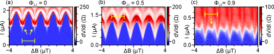
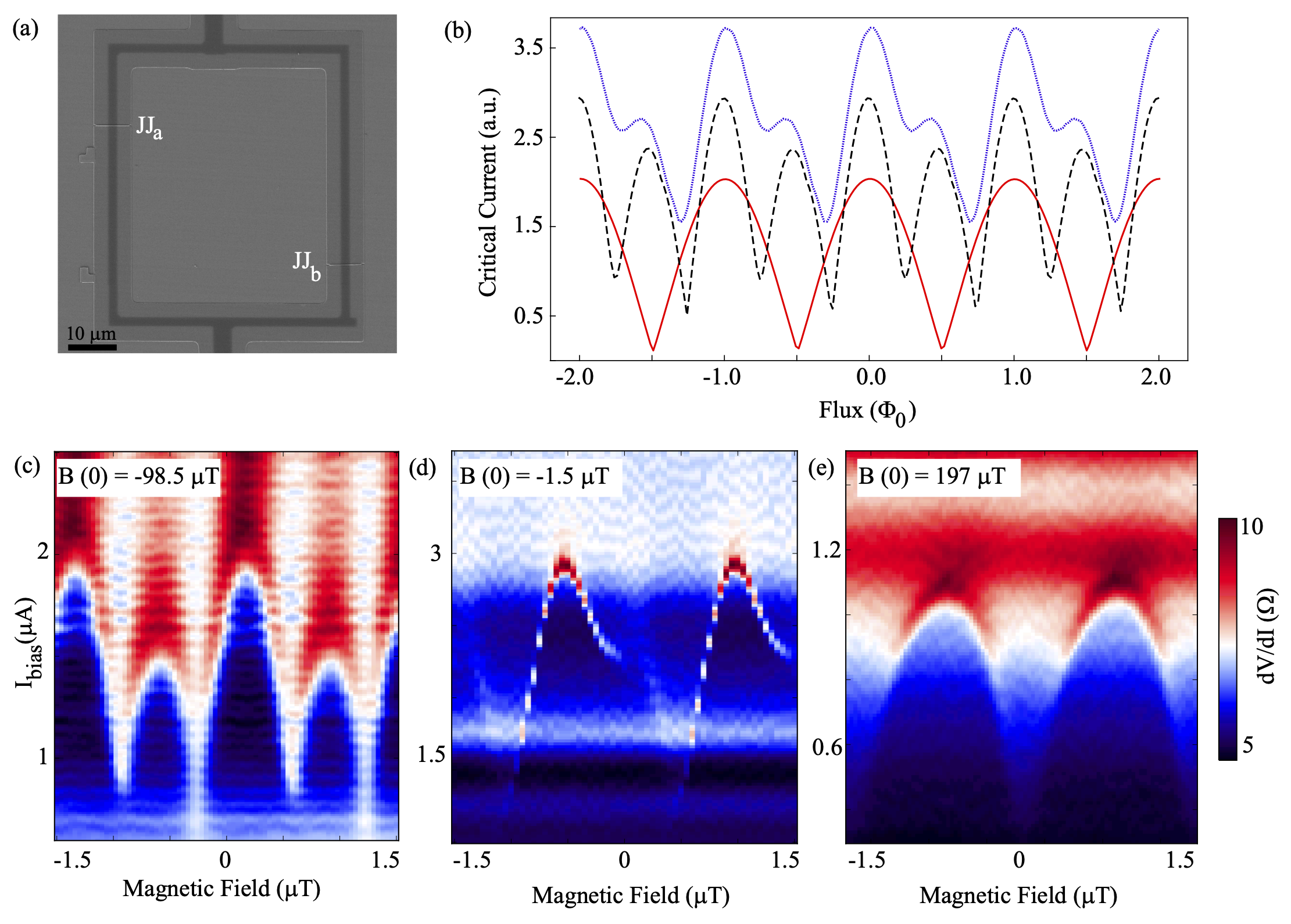
We first present examples of dc-SQUID patterns with extra features that we study in the context of the terms. Device SQUID-1 is depicted schematically in Fig. 1(a) and an optical microscope image is shown in Fig. 1(b). The device has two Josephson junctions in parallel, JJa and JJb. Two nanowire top-gates and are used for tuning critical currents. We set supercurrent to zero in one junction with its gate and measure the gate dependence of the switching current in the other junction [Fig. 1(c)]. is typically referred to as critical current, though the true Josephson critical current can be higher than the switching current. quenches at gate voltages near mV and saturates above 300 mV in both junctions. Both junctions have the same nominal geometry, so their magnetic flux modulation, or diffraction, patterns are expected to have similar periods. This can be confirmed in Fig. 1(d), where there is only one Fraunhofer-like low-frequency modulation while both junctions are in the superconducting state. With the Fraunhofer period of 0.29 mT and the junction width of 5 m, we get an effective junction length of 1.4 m (an order of magnitude larger than the typical physical length) for both JJs. The long effective length is likely due to large London penetration depth which is typical for thin film superconductors. We use the junction magnetic flux , given in the unit of . The SQUID flux and the junction flux are applied from a large superconducting magnet and cannot be independently controlled. The high frequency oscillations within the Fraunhofer-like envelope are due to interference between the two junctions. The period 1.57 T gives a SQUID area of m2 which is similar to the area of the inner loop ( m2). The oscillations are shown in detail in Fig. 2.

VII Figure 2 Description
SQUID-1 modulation patterns are shown in Figs. 2(a)-2(c) for different junction flux . Two junctions are tuned to have the same zero-field switching current so that the SQUID is symmetric ( A). At , the pattern exhibits kinks near SQUID oscillation minima [Fig. 2(a) yellow arrows, zoomed-in data in Fig. S9]. We also observe that, despite tuning the SQUID to the symmetric point, the nodes of the modulation patterns are lifted from zero. Pattern at [Fig. 2(b)] does not contain extra features. Here, follows a curve as expected for standard symmetric SQUID without high-order harmonics in its CPR. When is 0.9, the pattern has a distinct double-modulation character. Extra minima in are observed near half-period of SQUID modulation [Fig. 2(c) yellow arrow].
VIII Figure 3 Description
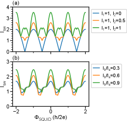
Next, we extract traces from data like in Fig. 2 and fit them to a basic model for a SQUID with two-harmonic CPR junctions (see supplementary materials for model description and detailed parameters [44]). The numerical model uses =0.4 the ratio between the second and the first Josephson harmonics in the CPR, for both junctions a and b.
In Fig. 3(a), the device is tuned to a symmetric state where the zero-field switching currents in JJa and JJb are similar ( A). As the junction flux increases, the amplitude of shifts towards lower values due to the Fraunhofer-like envelope. The model reproduces the basic features. Kinks, pointed out by single-ended arrows in panel (a), are most apparent near junction flux (zoomed-in data in Fig. S9). Node lifting (double arrows) is also reproduced by the model. While it is typically associated with asymmetric SQUIDs, in this model it originates from the second-order Josephson effect. Additional features disappear both in the data and in the model near , where the pattern closely follows the standard SQUID relation. When approaches 0.8 the experimental curve becomes skewed while the simulated curve is more symmetric.
In Fig. 3(b) SQUID-1 is tuned by gates, and is asymmetric while is 0. is fixed at A while is changing. The amplitude of the oscillation decreases as decreases. The oscillations are asymmetric. At A, two kinks (arrows) are at different heights. As decreases, one kink becomes difficult to resolve. In this case skewed patterns are captured by the model, e.g. at A. More examples of SQUID data are presented in supplementary materials from this device and additional SQUIDs [44].
IX Discussion of SQUID results
We first discuss the situation where . Our SQUID model shows that for a symmetric SQUID at , the nodes in are lifted from 0 and two additional kinks appear as increases [Fig. S3(a)]. These two signatures are highlighted in Fig. 3(a). Thus the presence of additional kinks, and the node lifting are consistent with a significant second harmonic.
As the SQUID is made more asymmetric in Fig. 3(b), the SQUID modulation appears more skewed, meaning that the y-axis position of one kink decreases while the position of the other increases. When , passes a nearly fixed supercurrent (thus a constant phase difference) to maximize the total switching current while the oscillation comes mostly from . As a result, traces out the CPR curve of with a constant shift. This regime is reached for A and 0.4 A. We notice that at A the kink is not resolved in the experimental curve but persists in the simulated curve. This may be due to a decrease in the junction transparency when is small which decreases the amplitude of the second harmonic in the CPR, but can also be due to the decreased accuracy of extraction at lower currents.
Near , oscillates like a function (Eq. S8) and shows no kinks or extra minima. The device looks like an ordinary SQUID. This is because at this junction flux value the second harmonic within each junction is cancelled. While the first harmonic has diffraction minima at , the second harmonic has nodes at where =0.
X Figure 4 Description

We also find second Josephson harmonic signatures in single junctions (Fig. 4). Similar results from other single JJs including those made from Sn/InAs 2DEG are available in Refs. [44, 42]. The overall envelope is Fraunhofer-like, which is standard for single-harmonic uniform and sinusoidal junctions. However, in deviation from this behavior, kinks are observed at half-integer magnetic flux values [Fig. 4(a) black arrows]. The kink is most clear within the first lobe of the Fraunhofer-like modulation. The second lobe is skewed which is consistent with a minor kink. The pattern is not symmetric in positive-negative field but is inversion symmetric in field-current four-quadrant view. This is consistent with the self-field effect in these extended junctions.
We extract and fit it with three different models in Fig. 4(b), detailed in supplementary materials [44]. The solid blue trace shows the basic Fraunhofer diffraction pattern for a single-component CPR. The two-component CPR model reproduces the kinks as shown in solid orange trace. Another model shown with dashed green line is for non-uniform critical current density and is discussed in the Alternative Explanations block.
Both non-uniformly distributed critical current and second harmonic in CPR produce half-period kinks. We notice that measured of the single junction is smaller than the simulated value near zero field. This may be due to a non-uniformly distributed supercurrent or the fact that the experimentally measured switching current is smaller than the theoretical critical current [45]. Because the fit does not reproduce the data simultaneously in the central lobe and in the side lobes, we do not rely on the values of extracted from this analysis (see supplementary materials for details [44]). Half-periodic kinks were observed in anodic-oxidation Al/2DEG junctions but the analysis of the second-order Josephson effect has not been performed [46].
XI Figure 5 Description

Shapiro steps in JJ-1 are presented at a microwave frequency of 6.742 GHz. A Shapiro step is a minimum in [Fig. 5(a)]. Another common form of plotting Shapiro step data is to bin data points by measured voltage across the junction [47]. In this form steps become straight bright lines in the histogram at Josephson voltages [Fig. 5(b)]. Apart from the usual integer steps, half-integer Shapiro steps are also observed at 3/2, 5/2 and 7/2. The missing step at 1/2 is likely due to self-heating [48, 49, 50].
While half-integer steps are clear and observed at relatively high frequencies, we do not observe steps at higher denominators such as 1/3 or 1/4. This is another confirmation that higher order Josephson harmonics, such as 3rd and 4th order, are not apparent in the data. Steps at 1/3 have been reported before in InSb nanowire junctions [51].
In these junctions we also observe missing integer steps at lower microwave frequencies, discussed in a separate manuscript [50]. This has been reported as a signature of the 4 Josephson effect characterized by the CPR. However, we observe the missing step pattern in the non-topological regime where fractional Josephson effect is not expected. We explain this through a combination of fine-tuning and low signal levels.
To illustrate that missing Shapiro steps are weak as evidence of unusual features in the CPR, we draw attention to the fact that the step at is missing from our data. We do not take this as evidence of an “integer” Josephson effect.
XII Figure 6 Discussion

Asymmetries between negative and positive switching currents in SQUIDs. The large second-order Josephson effect can produce asymmetries between positive and negative bias switching currents in junctions and SQUIDs [52, 53, 14, 34, 54]. These phenomena are heavily studied under the name “superconducting diode” in recent literature. To understand how the asymmetry arises we provide a simulation of our 2-junction 2-component CPR model in positive and negative bias (Figs. 6(a)). As can be seen, a kink in the positive bias is aligned with a dip in negative bias, and vice versa, an effect entirely due to the two-component CPR. This behavior is also present in the experiment (Fig. 6(b)). At the same time, the experimental data differ from the model in that the switching current maxima are not aligned for positive and negative bias in the experiment, but they are in the model. This difference is due to the finite inductance of the SQUID loop, of order 160 H, resulting in finite phase winding due to circulating currents, an inductive effect [55, 56]. This effect provides another mechanism for the asymmetry. The simulation including both the inductance and the second Josephson harmonic shows that increasing the inductance would suppress signatures due to the second harmonic, e.g., the kinks at quarter flux values (Fig. S6).
Sign of the second harmonic term. Simulation results in the main text do not include the inductive effect, therefore they do not reveal the sign of the second harmonic term. This is because is unchanged if both signs of the second harmonic term and the external flux are flipped [44]. The presence of finite SQUID inductance provides a simple way to determine the sign of the second harmonic term. The model combining both second harmonic and inductive effects shows that maxima in negative and positive s move towards kinks near half-integer flux values if the second-harmonic term is negative, and vice versa (Figs. S6(b) and S7(b)). The movement of maxima in the experiment (Fig. 6(b)) suggests a negative second harmonic term. This is expected if the second-order effect originates from high-transparency of the junction and from the skewed current-phase relation, which yields a negative second-order Fourier component. Note that the sign of the second-order term can also be determined by checking the directions of of the applied field and current flow.
XIII Alternative Explanations
Half-periodic kinks in a single JJ diffraction patterns can be explained by a non-uniformly distributed supercurrent. We reproduce these kinks with the model of a three-level supercurrent density distribution (Fig. 4(b) and supplementary materials [44]). The non-uniform supercurrent may be caused by resist residue introduced during fabrication. We observe stripes of residue in our first batch (Tab. S1, Al-chip-1) of junctions which includes JJ-1, caused by double electron beam exposure (Fig. S1). These residues are avoided and are not observed in newer devices without double exposure (Figs. 1(b),S23(b),S23(c)), which includes SQUID-1 and more devices in Fig. S23 and Ref. [42] - many of which do show additional modulation such as extra nodes and kinks.
It is worth noting that the non-uniform model produces a “lifted odd node” diffraction pattern that has been used to argue for the observation of the exotic fractional Josephson effect, characterized by 4-periodic current phase relations associated with Majorana modes [57]. We obtain the diffraction pattern of the same overall shape without the need to have this physics present [Fig. 4(b)]. In planar junctions it is difficult to know whether a node corresponds to integer or half-integer flux. This is because the junction area for supercurrent diffraction purposes can be much larger than the lithographic area. In our work, for instance, the junction length is close to 1.5 microns while the lithographic length is 150 nm. This makes it hard to distinguish a half-integer kink from a lifted integer node.
Another aspect we consider is whether patterns such as those extracted in Fig. 3 or Fig. 4(b) are true representations of the switching current evolution. In some of the junctions the apparent extra modulation (blue area in colorplots, highlighted in Fig. S24(c) by changing the color) appears to be above the true switching current and may arise due to the evolution of finite-voltage resonances in magnetic field. One origin for these resonances is multiple Andreev reflections (MAR). See Figs. S15-S18 for examples.
This type of artefacts does not explain all of our data. For example, in Fig. 4(a) we do not see MAR or faint finite-voltage state regions. Another argument we can give in support of the origins of the SQUID patterns is the detailed agreement between our numerical model and the data. See supplementary materials for an extended discussion [44].
Half-integer Shapiro steps have been attributed to effects not related to the second-order Josephson effect, such as a phase-locking of Josephson half-vortices to microwaves, and non-equilibrium quasiparticle dynamics [40, 41]. Hence their demonstration cannot by itself be used to claim the presence of terms. We provide Shapiro data as additional rather than key evidence.
Taken together, we argue that the evidence from SQUIDs, single junctions and agreement with the model, are all consistent with a strong second-order Josephson effect. While alternative explanations can be used to support individual measurements, none of them can explain all of the data, though multiple factors may be present simultaneously with a lower likelihood.
XIV Conclusion
In summary, we studied the current-phase relation in Josephson junctions and SQUIDs made with the nanowire shadow-mask method. Signatures due to a strong second-order harmonic in the CPR are observed. The simulation shows good agreement to experimental data in the SQUID device suggesting a ratio of the second to first harmonics of .
In the clean limit and at zero temperature, the CPR is a skewed 2-periodic function [6] with many higher order terms. After Fourier decomposition, one gets and . So, in an ideal ballistic junction, the magnitude of the second harmonic we obtain would not necessarily be surprising. The surprising is the combination of doubly-modulated junction characteristics together with the lack of manifested higher order terms such as the third term. This indicates an unusual situation in which either the second order term is unusually large, or the higher order terms are suppressed through an undetermined mechanism.
XV Future work
The origin of such a strong second-order harmonic, not accompanied by even higher order terms (skewed CPR) still needs to be understood. The sensitivity of observed signatures to surface treatment can be studied. Higher harmonics can be used to engineer nonlinearity in quantum circuits.
XVI Duration and Volume of Study
This study is divided into two periods, which correspond to period 2 and period 3 in Ref. [42].
The first period was between August 2018 to June 2019, including sample preparation, device fabrication and measurements. We explored the first-generation devices (Al, InSb nanowire, without gates). More than 7 devices on 1 chip are measured during 2 cooldowns in a dilution refrigerator, producing about 8900 datasets.
The second period was between March 2021 to February 2022. We explored the second-generation devices, (Al or Sn, InAs/HfOx nanowire, with self-aligned nanowire gates). 62 devices on 6 chips are measured during 8 cooldowns in dilution refrigerators, producing about 5700 datasets.
XVII Data availability
Curated library of data extending beyond what is presented in the paper, as well as simulation and data processing code are available at [58].
XVIII Acknowledgements
We thank J. Stenger, D. Pekker, D. Van Harlingen for discussions. We thank E. Bakkers, G. Badawy and S. Gazibegovic for providing InSb nanowires. We acknowledge the use of shared facilities of the NSF Materials Research Science and Engineering Center (MRSEC) at the University of California Santa Barbara (DMR 1720256) and the Nanotech UCSB Nanofabrication Facility.
XIX Funding
Work supported by the ANR-NSF PIRE:HYBRID OISE-1743717, NSF Quantum Foundry funded via the Q-AMASE-i program under award DMR-1906325, the Transatlantic Research Partnership and IRP-CNRS HYNATOQ, U.S. ONR and ARO.
XX References
References
- Fu and Kane [2008] L. Fu and C. L. Kane, Physical review letters 100, 096407 (2008).
- Pientka et al. [2017] F. Pientka, A. Keselman, E. Berg, A. Yacoby, A. Stern, and B. I. Halperin, Physical Review X 7, 021032 (2017).
- Casparis et al. [2018] L. Casparis, M. R. Connolly, M. Kjaergaard, N. J. Pearson, A. Kringhøj, T. W. Larsen, F. Kuemmeth, T. Wang, C. Thomas, S. Gronin, et al., Nature nanotechnology 13, 915 (2018).
- Khaire et al. [2010] T. S. Khaire, M. A. Khasawneh, W. Pratt Jr, and N. O. Birge, Physical review letters 104, 137002 (2010).
- Likharev [1979] K. Likharev, Reviews of Modern Physics 51, 101 (1979).
- Golubov et al. [2004] A. A. Golubov, M. Y. Kupriyanov, and E. Il’Ichev, Reviews of modern physics 76, 411 (2004).
- Willsch et al. [2023] D. Willsch, D. Rieger, P. Winkel, M. Willsch, C. Dickel, J. Krause, Y. Ando, R. Lescanne, Z. Leghtas, N. T. Bronn, et al., arXiv preprint arXiv:2302.09192 (2023).
- Kulik and Omel’Yanchuk [1975] I. Kulik and A. Omel’Yanchuk, Soviet Journal of Experimental and Theoretical Physics Letters 21, 96 (1975).
- Spanton et al. [2017] E. M. Spanton, M. Deng, S. Vaitiekėnas, P. Krogstrup, J. Nygård, C. M. Marcus, and K. A. Moler, Nature Physics 13, 1177 (2017).
- Murani et al. [2017] A. Murani, A. Kasumov, S. Sengupta, Y. A. Kasumov, V. Volkov, I. Khodos, F. Brisset, R. Delagrange, A. Chepelianskii, R. Deblock, et al., Nature communications 8, 1 (2017).
- Ginzburg et al. [2018] L. V. Ginzburg, I. Batov, V. Bol’ginov, S. V. Egorov, V. Chichkov, A. E. Shchegolev, N. V. Klenov, I. Soloviev, S. V. Bakurskiy, and M. Y. Kupriyanov, JETP Letters 107, 48 (2018).
- Kayyalha et al. [2019] M. Kayyalha, M. Kargarian, A. Kazakov, I. Miotkowski, V. M. Galitski, V. M. Yakovenko, L. P. Rokhinson, and Y. P. Chen, Phys. Rev. Lett. 122, 047003 (2019).
- Kayyalha et al. [2020] M. Kayyalha, A. Kazakov, I. Miotkowski, S. Khlebnikov, L. P. Rokhinson, and Y. P. Chen, npj Quantum Materials 5, 1 (2020).
- Mayer et al. [2020] W. Mayer, M. C. Dartiailh, J. Yuan, K. S. Wickramasinghe, E. Rossi, and J. Shabani, Nature communications 11, 1 (2020).
- Nichele et al. [2020] F. Nichele, E. Portolés, A. Fornieri, A. M. Whiticar, A. C. C. Drachmann, S. Gronin, T. Wang, G. C. Gardner, C. Thomas, A. T. Hatke, M. J. Manfra, and C. M. Marcus, Phys. Rev. Lett. 124, 226801 (2020).
- Endres et al. [2023] M. Endres, A. Kononov, H. S. Arachchige, J. Yan, D. Mandrus, K. Watanabe, T. Taniguchi, and C. Schönenberger, Nano Letters (2023).
- Babich et al. [2023] I. Babich, A. Kudriashov, D. Baranov, and V. Stolyarov, arXiv preprint arXiv:2302.02705 (2023).
- Kitaev [2001] A. Y. Kitaev, Physics-Uspekhi 44, 131 (2001).
- Beenakker [2013] C. Beenakker, Annu. Rev. Condens. Matter Phys. 4, 113 (2013).
- Baselmans et al. [2002] J. Baselmans, T. Heikkilä, B. Van Wees, and T. Klapwijk, Physical review letters 89, 207002 (2002).
- Frolov et al. [2004] S. Frolov, D. Van Harlingen, V. Oboznov, V. Bolginov, and V. Ryazanov, Physical Review B 70, 144505 (2004).
- Goldobin et al. [2007] E. Goldobin, D. Koelle, R. Kleiner, and A. Buzdin, Physical Review B 76, 224523 (2007).
- van Dam et al. [2006] J. A. van Dam, Y. V. Nazarov, E. P. Bakkers, S. De Franceschi, and L. P. Kouwenhoven, Nature 442, 667 (2006).
- Cleuziou et al. [2006] J.-P. Cleuziou, W. Wernsdorfer, V. Bouchiat, T. Ondarçuhu, and M. Monthioux, Nature nanotechnology 1, 53 (2006).
- Stoutimore et al. [2018] M. Stoutimore, A. Rossolenko, V. Bolginov, V. Oboznov, A. Rusanov, D. Baranov, N. Pugach, S. Frolov, V. Ryazanov, and D. Van Harlingen, Physical review letters 121, 177702 (2018).
- Walker and Luettmer-Strathmann [1996] M. Walker and J. Luettmer-Strathmann, Physical Review B 54, 588 (1996).
- Il’ichev et al. [1999] E. Il’ichev, V. Zakosarenko, R. IJsselsteijn, H. Hoenig, V. Schultze, H.-G. Meyer, M. Grajcar, and R. Hlubina, Physical Review B 60, 3096 (1999).
- Il’ichev et al. [2001] E. Il’ichev, M. Grajcar, R. Hlubina, R. P. J. IJsselsteijn, H. E. Hoenig, H.-G. Meyer, A. Golubov, M. H. S. Amin, A. M. Zagoskin, A. N. Omelyanchouk, and M. Y. Kupriyanov, Phys. Rev. Lett. 86, 5369 (2001).
- Zhao et al. [2021] S. Zhao, N. Poccia, X. Cui, P. A. Volkov, H. Yoo, R. Engelke, Y. Ronen, R. Zhong, G. Gu, S. Plugge, et al., arXiv preprint arXiv:2108.13455 (2021).
- Zhu et al. [2021] Y. Zhu, M. Liao, Q. Zhang, H.-Y. Xie, F. Meng, Y. Liu, Z. Bai, S. Ji, J. Zhang, K. Jiang, R. Zhong, J. Schneeloch, G. Gu, L. Gu, X. Ma, D. Zhang, and Q.-K. Xue, Phys. Rev. X 11, 031011 (2021).
- Vanneste et al. [1988] C. Vanneste, C. Chi, W. Gallagher, A. Kleinsasser, S. Raider, and R. Sandstrom, Journal of applied physics 64, 242 (1988).
- de Lange et al. [2015] G. de Lange, B. van Heck, A. Bruno, D. J. van Woerkom, A. Geresdi, S. R. Plissard, E. P. A. M. Bakkers, A. R. Akhmerov, and L. DiCarlo, Phys. Rev. Lett. 115, 127002 (2015).
- Larsen et al. [2020] T. W. Larsen, M. E. Gershenson, L. Casparis, A. Kringhøj, N. J. Pearson, R. P. G. McNeil, F. Kuemmeth, P. Krogstrup, K. D. Petersson, and C. M. Marcus, Phys. Rev. Lett. 125, 056801 (2020).
- Ciaccia et al. [2023] C. Ciaccia, R. Haller, A. C. Drachmann, C. Schrade, T. Lindemann, M. J. Manfra, and C. Schönenberger, arXiv preprint arXiv:2304.00484 (2023).
- Valentini et al. [2023] M. Valentini, O. Sagi, L. Baghumyan, T. de Gijsel, J. Jung, S. Calcaterra, A. Ballabio, J. A. Servin, K. Aggarwal, M. Janik, et al., arXiv preprint arXiv:2306.07109 (2023).
- Kitaev [2006] A. Kitaev, arXiv preprint cond-mat/0609441 (2006).
- Brooks et al. [2013] P. Brooks, A. Kitaev, and J. Preskill, Physical Review A 87, 052306 (2013).
- Gyenis et al. [2021] A. Gyenis, A. Di Paolo, J. Koch, A. Blais, A. A. Houck, and D. I. Schuster, PRX Quantum 2, 030101 (2021).
- Sellier et al. [2004] H. Sellier, C. Baraduc, F. Lefloch, and R. Calemczuk, Phys. Rev. Lett. 92, 257005 (2004).
- Frolov et al. [2006] S. M. Frolov, D. J. Van Harlingen, V. V. Bolginov, V. A. Oboznov, and V. V. Ryazanov, Phys. Rev. B 74, 020503(R) (2006).
- Lehnert et al. [1999] K. W. Lehnert, N. Argaman, H.-R. Blank, K. C. Wong, S. J. Allen, E. L. Hu, and H. Kroemer, Phys. Rev. Lett. 82, 1265 (1999).
- Zhang et al. [2022a] P. Zhang, A. Zarassi, M. Pendharkar, J. S. Lee, L. Jarjat, V. van de Sande, B. Zhang, S. Mudi, H. Wu, S. Tan, C. P. Dempsey, A. P. McFadden, S. D. Harrington, B. Shojaei, J. T. Dong, A. H. Chen, M. Hocevar, C. J. Palmstrøm, and S. M. Frolov, arXiv preprint arXiv:2211.04130 (2022a).
- Zarassi [2020] A. Zarassi, From Quantum Transport in Semiconducting Nanowires to Hybrid Semiconducting-Superconducting Qubits, Ph.D. thesis, University of Pittsburgh (2020).
- [44] See Supplementary Materials for detailed models, extended data, and more discussion .
- Mayer et al. [2019] W. Mayer, J. Yuan, K. S. Wickramasinghe, T. Nguyen, M. C. Dartiailh, and J. Shabani, Applied Physics Letters 114, 103104 (2019).
- Drachmann et al. [2021] A. C. Drachmann, R. E. Diaz, C. Thomas, H. J. Suominen, A. M. Whiticar, A. Fornieri, S. Gronin, T. Wang, G. C. Gardner, A. R. Hamilton, et al., Physical Review Materials 5, 013805 (2021).
- Bocquillon et al. [2017] E. Bocquillon, R. S. Deacon, J. Wiedenmann, P. Leubner, T. M. Klapwijk, C. Brüne, K. Ishibashi, H. Buhmann, and L. W. Molenkamp, Nature Nanotechnology 12, 137 (2017).
- De Cecco et al. [2016] A. De Cecco, K. Le Calvez, B. Sacépé, C. B. Winkelmann, and H. Courtois, Phys. Rev. B 93, 180505 (2016).
- Shelly et al. [2020] C. D. Shelly, P. See, I. Rungger, and J. M. Williams, Physical Review Applied 13, 024070 (2020).
- Zhang et al. [2022b] P. Zhang, S. Mudi, M. Pendharkar, J. Lee, C. Dempsey, A. McFadden, S. Harrington, J. Dong, H. Wu, A.-H. Chen, et al., arXiv preprint arXiv:2211.08710 (2022b).
- Zuo et al. [2017] K. Zuo, V. Mourik, D. B. Szombati, B. Nijholt, D. J. Van Woerkom, A. Geresdi, J. Chen, V. P. Ostroukh, A. R. Akhmerov, S. R. Plissard, et al., Physical review letters 119, 187704 (2017).
- Fominov and Mikhailov [2022] Y. V. Fominov and D. S. Mikhailov, Phys. Rev. B 106, 134514 (2022).
- Souto et al. [2022] R. S. Souto, M. Leijnse, and C. Schrade, Phys. Rev. Lett. 129, 267702 (2022).
- Zhang et al. [2022c] B. Zhang, Z. Li, V. Aguilar, P. Zhang, M. Pendharkar, C. Dempsey, J. Lee, S. Harrington, S. Tan, J. Meyer, et al., arXiv preprint arXiv:2212.00199 (2022c).
- Paolucci et al. [2023] F. Paolucci, G. De Simoni, and F. Giazotto, Applied Physics Letters 122, 042601 (2023), https://doi.org/10.1063/5.0136709 .
- Tesche and Clarke [1977] C. D. Tesche and J. Clarke, Journal of Low Temperature Physics 29, 301 (1977).
- Williams et al. [2012] J. Williams, A. Bestwick, P. Gallagher, S. S. Hong, Y. Cui, A. S. Bleich, J. Analytis, I. Fisher, and D. Goldhaber-Gordon, Physical review letters 109, 056803 (2012).
- [58] DOI: 10.5281/zenodo.6416083 .
Supplementary Materials: Large Second-Order Josephson Effect in Planar Superconductor-Semiconductor Junctions
XXI Author contributions
A.-H.C, H.W., and M.H. grew InAs nanowires and the dielectric layer. M.P., J.S.L., C.P.D., A.P.M., S.D.H., J.T.D., and C.J.P. grew quantum wells and superconducting films. A.Z. and P.Z. fabricated devices. L.J., V.V.d.S., A.Z., and P.Z. performed measurements. L.J. and P.Z. did the simulation. A.Z. and L.J. prepared draft versions of this manuscript. P.Z. and S.M.F. wrote the manuscript with inputs from all authors.
XXII Device information
| Name | Chip name | Reference code | Name in Ref. [42] | Superconductor | Shadow wire |
|---|---|---|---|---|---|
| SQUID-1 | Al-chip-3 | 20210924 Al InAs 2DEG 4.10 | SQUID-1 | Al | InAs |
| JJ-1 | Al-chip-1 | 2019 2DEG 9 | JJ-S3 | Al | InSb |
| SQUID-S1 | Al-chip-2 | 210329 Al InAs 2DEG 6.8 | - | Al | InAs |
| SQUID-S2 | Sn-chip-2 | 20211009 Sn InAs 2DEG 7.7 | - | Sn | InAs |
| SQUID-S3 | Al-chip-1 | 2019 2DEG 16 | - | Al | InSb |
| JJ-S1 | Al-chip-1 | 2019 2DEG 10 | JJ-S4 | Al | InSb |
| JJ-S2 | Al-chip-2 | 210329 Al InAs 2DEG 7.5b | JJ-S9 | Al | InAs |
| JJ-S3 | Sn-chip-2 | 20211009 Sn InAs 2DEG 9.8a | JJ-2 | Sn | InAs |
XXIII Models for a single JJ
The magnetic field induces an extra phase variation inside the junction (Eq. S3), leading to the supercurrent interference. The switching current () of a single JJ in a magnetic field can be written as
| (S1) | |||||
| (S2) | |||||
| (S3) |
where is the magnetic flux in the junction normalized by the superconducting flux quantum (), is the phase difference which is a free parameter here for calculating , is the width (perpendicular to the direction of the current) of the junction, and are amplitudes of the first- and second-order harmonics in the CPR ( can be regarded as the global current and as the current density), we ignore higher-order harmonics in our model, is the position in the direction. The integration in Eq. S2 is independent of , so we can set for simplicity.
If is a constant and , Eq. S2 can be simplified as
| (S4) |
and reduces to which resembles the Fraunhofer diffraction.
Three models for JJs are used in Fig. 4(b):
-
1.
CPR has only the 1st harmonic, , .
-
2.
CPR has 1st and 2nd harmonics, , .
-
3.
CPR has only the 1st harmonic and is non-uniformly distributed. In this model, is a three-step piece-wise function. It equals to in the middle () and on two sides.
XXIV More JJ simulations


XXV Non-inductive SQUID model
As sketched in Fig. 1(a), a SQUID consists of two JJs, i.e., JJa and JJb. We denote magnetic fluxes (normalized by ) in the enclosed area of the SQUID, JJa, and JJb by , and . Here and are ratios between the SQUID-enclosed area and junction areas. We denote amplitudes of harmonics in JJa and JJb by , , , .
| (S5) | |||||
| (S6) | |||||
| (S7) |
where . and are junction widths. The integration terms are independent of widths because and are absorbed under the transformation .
In the simplest situation, i.e, , two junctions are identical, and there is only the first harmonic in the CPR, reduces to
| (S8) |
which is a high-frequency SQUID oscillation (the cosine term) modulated by a low-frequency Fraunhofer oscillation ().
In our simulation, we assume is a constant independent of the junction index and the gate voltage. Parameters used for SQUID-1 in Fig. 3 are as follows, , , , . is extracted from periods of the JJ oscillation and the SQUID oscillation. is the measured zero-field switching current in junction [Fig. 1(c)]. is a fitting parameter which is chosen to be in Fig. 3(a) and in Fig. 3(b). The difference in may arise due to the uncertainty in tuning nominal switching currents by gates or higher-order harmonics that are not considered in the simulation.
XXVI More SQUID simulations

XXVII Inductive SQUID
We model the inductive SQUID following Ref. [56], but including higher order terms. The currents through junctions a and b are:
| (S9) | |||||
| (S10) |
where and are phase differences in junctions a and b, respectively. is the amplitude of the second harmonic. For simplicity, we use normalized currents, and . The total current and circulating current are:
| (S11) | |||||
| (S12) |
and are connected by the equation:
| (S13) |
where is the normalized flux applied by the external field, is the normalized inductance, is an arbitrary integer. Here we ignore the inductance difference between the two arms of the SQUID for simplicity. A more general case can be found in Ref. [56]. Note that when , is different from the critical current by a factor . We should use instead of to compare with the experimental parameters.
The maximized (minimized) is achieved when both and are maximized (minimized), which gives , , , () for the maximum (minimum). The external fluxes where reaches maximum (minimum) can be calculated by substituting these into Eq. S13:
| (S14) |
The dependence of critical current on is calculated using the following procedure. First, at every , we search for pairs satisfying Eq. S13. Second, we find the minimum and maximum currents among valid pairs, which are the negative and positive critical currents. The results of inductive modeling can be found in Figs. S5 and S6.


XXVIII Sign of the second harmonic term
In the JJ model and the non-inductive SQUID model, changing the sign of the second harmonic term is equivalent to changing the sign of the external flux. This is because Eqs. S2 and S6 are unchanged under the transformation and , respectively.
In the inductive SQUID model, changing the sign of the second harmonic term is equivalent to changing both signs of the external flux and the normalized inductance . This is because Eqs. S9 and S10 are unchanged under the transformation .

.

.
XXIX Supplementary data from SQUID-1


XXX Data from SQUIDs not shown in the main text


XXXI Supplementary data from JJs not shown in the main text


