figure \MakeSortedtable
Instinctual Interference Adaptation in a Low-Power High-Linearity Receiver With Combined Feedforward and Feedback Control
Sub-1ms Instinctual Interference Adaptation in a Low-Power High-Linearity Receiver With Feedforward and Feedback Control Systems (Need Change
Sub-1ms Instinctual Interference Adaptive GaN LNA Front-End with Power and Linearity Tuning
Abstract
One of the major challenges in communication, radar, and electronic warfare receivers arises from nearby device interference. The paper presents a 2-6 GHz GaN LNA front-end with onboard sensing, processing, and feedback utilizing microcontroller-based controls to achieve adaptation to a variety of interference scenarios through power and linearity regulations. The utilization of GaN LNA provides high power handling capability (30 dBm) and high linearity (OIP3= 30 dBm) for radar and EW applications. The system permits an LNA power consumption to tune from 500 mW to 2 W (4X increase) in order to adjust the linearity from P1dB,IN=-10.5 dBm to 0.5 dBm (>10X increase). Across the tuning range, the noise figure increases by approximately 0.4 dB. Feedback control methods are presented with backgrounds from control theory. The rest of the controls consume 10 (100 mW) of nominal LNA power (1 W) to achieve an adaptation time <1 ms.
Index Terms:
GaN LNA, adaptive control, front-end, interference robust.I Introduction
With continuous advances in communication, radar, and electronic warfare (EW) technologies, the receivers (Rx) are becoming more susceptible to nearby interferences. Unlike the intentional jamming that deliberately saturates the receiver system to produce an unusable signal, unintentional interferences are more prevalent such as self-interference, and adjacent channel interference and reflection by neighboring devices[2, 3]. To combat unintentional interferences, some of today’s receivers are designed to operate in the worst-case condition at the cost of extra power consumption. When the radar and EW receivers are implemented in large arrays, the extra power consumption can quickly add up and may require extra cooling. The increasing interferences caused extra power consumption calls for an adaptive interference-tolerant low-power RF Rx system.
The first step to the adaptive interference-tolerant low-power RF receiver system especially in the radar and EW receivers is the ability to sustain a high input level. GaN LNAs have been widely used due to their higher power handling capabilities (>30 dBm) than traditional GaAs or CMOS LNAs (20 dBm). Traditional LNAs usually require the implementation of a limiter in the input path for protection from high input power while the GaN LNA is able to function standalone [3]. The next step is the ability to adjust the receiver power consumption according to the input power as opposed to continuous operation under worse-case conditions. Operation of the receiver system in low-power mode can significantly reduce the power consumption and the need for cooling when the input is small in a large radar and EW receiver array.
I-A Background of Adaptive Receivers and Related Works
In the effort of achieving a low-power and interference adaptive Rx, some previous works have focused on linearizing mixers using frequency translation by compressing third-order intermodulation product (IM3) [4, 5, 6]; however, if the Low-Noise Amplifiers (LNA) are already saturated, linearizing the later stages gains little advantage. Other works contributed on creating ultra-low-power LNA using the current reuse and forward body biasing techniques [7, 8, 9], variable-gain LNA [10, 11, 12, 13], an orthogonally tunable LNA where input third-order intercept point (IIP3) and gain can be individually changed through the bias tuning knobs [14], or a combination of low-power and variable-gain LNA [15]. The variable gain and IIP3 in the design of LNA can assist the receiver to become more interference tolerant in terms of both large signal saturation and small signal nonlinearity; however, these works only included circuit level designs without a complete system design. With the purpose of developing an adaptive receiver, dynamic bias (tuning of the gate and drain voltage) for the optimization of the signal-to-noise and distortion (SNDR) for a Gallium-Nitride (GaN) LNA is explored in [16]; however, the system-level considerations for the dynamic bias technique were not included.
In [17], the authors utilized the orthogonally tunable LNA to implement a use-aware adaptive RF transceiver system where different low-power adaptation modes are designed for different throughput requirements but disregard the tuning speed of the Rx. Other implementations of an adaptive RF communication system use error vector magnitude (EVM) and look up table (LUT) with stored tuning conditions for the LNA and mixer to optimally trade off power and performance [18]. Advancements were made later by considering the process variation of the components with tuning adjustments included in the design process [19]. These contributions provide a thorough design of the Rx system, but most of the results are still simulation-based, and utilization of only the LUT does not provide local feedback for further tuning of the system.
I-B Proposed solution
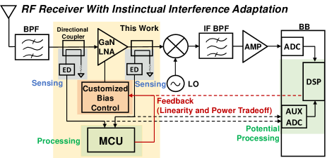
This paper presents the first building block, a high input tolerant and interference adaptive GaN LNA front-end, to an instinctual adaptive receiver. Fig. 1 modifies the traditional RF receiver with the instinctual interference adaptation by incorporating 1) sensing through the onboard envelope detectors as observation points at the input and/or output of the GaN LNA, 2) processing through localized digital processing unit or the auxiliary ADC that’s already present in baseband(BB), and 3) feedback to the customized GaN LNA bias controls for the best linearity and power performance while maintaining signal integrity. Note that in this paper, the processing is done using an MCU, but it can also be done using the BB DSP and auxiliary ADC. When blockers are present in a traditional Rx system working in nominal conditions, the blockers would saturate the LNA and produce a comparable IM3 to the actual signal which results in an undecidable LNA output. When blockers are present in the front-end with instinctual interference adaptation, the control logic would be able to increase the linearity of the system which in turn increases the IM3 compression at the cost of power consumption. When the signal and interference are both low, the Rx with bias control would be consuming less power for approximately the same signal levels. Note that the need for a better linearity range is present regardless of whether the high power is from the desired signal or the interference as long as the system is able to be brought back to the linearity range.
To have a higher power handling capability and linearity, GaN LNA is utilized. Our prior work [1] involves interference adaptation for an Rx system with incremental adaptation control involving both feedforward and feedback path for the GaN LNA. However, the utilization of bench-top equipment significantly increases the adaptation time and the form factor of the system, which makes the design unsuitable in real life. [1] also lacks the consideration of the effects of the GaN LNA properties.
This paper builds upon the prior work and has the following additional contributions:
-
•
This work implements the first sub-1ms interference adaptive, instinctual GaN LNA system with a localized in-built intelligence using a microcontroller. The system consumes 10 of nominal LNA power to provide a wide tuning range of linearity for about 11 dB and LNA power for 0.5-2 W.
-
•
The control circuitry of GaN LNA has been designed with careful consideration of the high-power effects of GaN LNA and the trade-off between system adaptation time and device lifetime.
-
•
Background control theory of the system is provided on the limitations for the overall adaptation time (< 1 ms) which shows a high correlation with the measurement results. To the authors’ current knowledge, this is the first control theory introduced for an interference adaptive RF front-end system.
-
•
Important trade-offs are presented between two designs: 1) feedforward + feedback using control theory mentioned in Sec. IV-E and 2) feedback only using i) incremental adaptation, ii) lookup table (LUT) and iii) one-shot + incremental adaptations. The different designs illustrate different timing constraints and complexities for different applications.
The paper is organized as follows: Sec. II provides an overview of the control loops and component characterization; Sec. III investigates different design considerations such as the design of directional coupler, high input power effects for a GaN LNA, Gate Voltage (VG) based tuning method and design comparison; Sec. IV describes the three control methods and the control theory; Sec. V presents the measurement results and Sec. VI presents the future directions of this work.
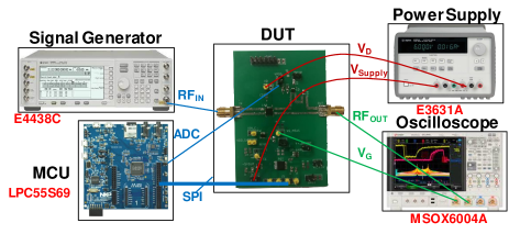
II Hardware Description and Characterization
II-A System Architecture and PCB Designs
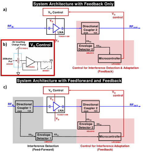
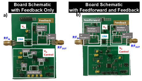
The two-layer PCB utilizes Rogers 4003C material with a thickness of 0.508 mm. The signal lines are carefully matched to 50 . The system architectures are shown in Fig. 2 with associated board layouts shown in Fig. 3. The commercial off-the-shelf parts (COTS) used on the PCBs are listed in Table 1. Fig. 2a) and 3a) show the architecture and layout for the feedback-only design where the interference detection and adaptation are performed in the feedback loop that utilizes an envelope detector (ED) to sample the output of the LNA. The bias control circuitry for the LNA is shown in Fig. 2b). Fig. 2c) and 3b) show the architecture and layout for the feedforward and feedback design. The feedforward loop involves the use of envelope detector 1 (ED1) that’s higher in sensitivity than envelope detector 2 (ED2) used in the feedback loop while still able to sustain the maximum input signal limited by the rating of the LNA at 30 dBm (1W). The difference between the two designs is how the interference will be detected (through the feedforward and feedback path, or directly from the feedback path) which will be discussed more in later sections.
The directional couplers and the LNA forms the front end in the system that will be connected to a mixer and baseband stages in a standard RF receiver. For a combined feedforward and feedback system, RF input first passes the through port of the directional coupler 1 to the LNA while the coupling port enables ED1 to measure the input signal level. Directional couplers are necessary for measurement because of the physical constraints (power handling capability) of the EDs as well as to avoid a significant power divide from the LNA. If the input signal is high (i.e. a blocker), then ED1 will output a higher DC voltage. The assumption is that high-level input signals are only caused by the interference and not the desired signal, thus high input signal corresponds to a high interference level. ED2 in the feedback path will also be incorporated in the interference detection for a better sensitivity after the LNA gain. The measurement will be processed through the ADC on the microcontroller and if the microcontroller determines the adaptation of the LNA is needed, tuning control will be initiated. The feedback control adjusts the gate voltage (VG) of the LNA to achieve the high linearity for the LNA which will be further discussed in Sec. IV. Note that the drain voltage (VD) of the LNA is not being controlled because the linearity improvement is minimal with changing VD for the specific LNA presented; however, VD controllability can be considered for future improvements on other LNAs. The difference with a feedback-only system is that the presence of the interference will only be detected using ED2 in the feedback loop.
II-B Characterization of Components
| Component | Part Number | Specifications |
|---|---|---|
| GaN LNA | TGA2611-SM (Qorvo) [28] | 2-6GHz, 1dB NF, 22dB Gain, -4dBm P1dB,IN, 1W nominal power |
| Envelope Detector 1 | LMH2120 [29] | 0.05-6GHz, 7s trise, 2.9mA 0.032V-1.1V Vout, 50 PIN=-4012dBm |
| Envelope Detector 2 | ADL6010 [30] | 0.5-43.5GHz, 47s trise, 1.6mA, 0.01V-3V Vout, 50 PIN=-3015dBm |
| -5V Inverting Charge Pump | LTC1983-5[31] | -5V Vout, 25A |
| Digitally Programmed Potentiometer | AD5260[32] | 200k, dual-supply, 256taps, 4-wire SPI, 0.3mW, tsettling=5s |
| Operational Amplifier | LTC6255[33] | 60A, 6MHz GBP, 1.5V/us, 2.5Vpp eni |
| Switch | ADG601[34] | 2.5ohm, 1A, 80ns ton, 45ns toff, N.O., -60dB off isolation |
| Micro- controller | LPC55S69[35] | 16bit ADC, 1MHz fsample (ADC), SPI support, 150MHz fCLK |
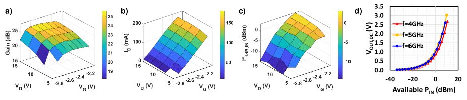
The components used are described in Table I. The LNAs in both the MWCL [1] and this paper are the same part number, but there are some chip-to-chip variations such that with the same VG, ID is higher in this paper. Note that the characteristics of the GaN LNA are determined more by the current rather than the bias voltage. This is because diodes are important in the GaN LNA modeling, and biasing the diode current with the correct voltage is more important [36]. We decided to continue with the VG range of -2.7 V to -2.2 V with a higher ID due to a worse S11 response at VG < -2.7 V as shown in Sec.V-C. The feedforward and feedback path components are characterized in the 2-6 GHz range. The losses due to the SMA cables are calibrated during the characterization of the RF components and measurements thereafter. RF components are chosen to have an input impedance of 50 . Fig. 4a)-c) represent the behavior of a GaN LNA at 4 GHz. As LNA’s VG increases from -2.8 V to -2.2 V, the gain first increases and saturates at around -2.5 V, then starts to decrease. The gain also increases with increasing VD. Because the change in gain is less than 4 dB (neglecting the -2.8 V VG data due to low gain and P1dB,IN, the adaptation will be between VG=-2.7 V to -2.1 V), the LNA gain is a weak function of both VD and VG. The supply current (ID) increases by more than a hundred mA with increasing VG while having a small change with increasing VD. This makes LNA’s ID a strong function of VG and a weak function of VD. The input P1dB (P1dB,IN) of the LNA varies around 16.5 dBm with increasing VG but changes minimally with VD. This makes the LNA’s P1dB,IN a strong function of VG and a weak function of VD. Therefore, only VG will be changed in the later sections to achieve linearity while VD is fixed at 10 V. Note that if the LNA’s P1dB,IN response is both a strong function of VG and VD, or if the LNA’s gain is a strong function of VD, both VG and VD can be implemented in the control loop.
Fig. 4d) represents the behavior of ED2 at frequencies of 4, 5, and 6 GHz. The voltage output of ED2 increases exponentially with increasing power. ED1 is chosen to be able to detect low power levels at the input. Other controlling components listed in Table I are generally chosen to be low power, short settling and rising time, and low noise.
III Design Considerations
III-A Directional Coupler Design
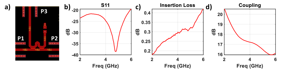
In our prior work [1], we utilized COTS directional coupler components to provide the measurement path; however, even though the components have outstanding specs, the integration of the directional coupler with the PCB board is causing unwanted reflections from the soldering and the abrupt transition from the trace to the component. Consequently, this paper takes advantage of the onboard microstrip design for the directional coupler which avoids extra transition from the board to the component. The coupler is necessary for decreasing the power input to below the power limit of the envelope detector and not to diverge extra power from the signal path for measurement purposes. The microstrip directional coupler schematic is shown in Fig. 5a) [37]. The measurements for the directional coupler are shown in 5b)-d). The S11 shows low return loss with measurements below -19 dB over the frequency from 2 GHz to 6GHz. The insertion loss (S21) increases from 0.18 dB to 0.42 dB with frequency. The coupling (S31) changes from 20.5 dB to 16 dB over the bandwidth.
III-B GaN LNA Considerations for High Power Input
Unlike the typical GaAs LNA’s lifetime being limited by the breakdown voltage, GaN LNA is limited by high DC gate current and drain-gate voltage (VDG). Characteristics of a GaN LNA with high input power have been investigated in [38]. Similar characteristics have been presented for the LNA used in this paper in Fig. 6.
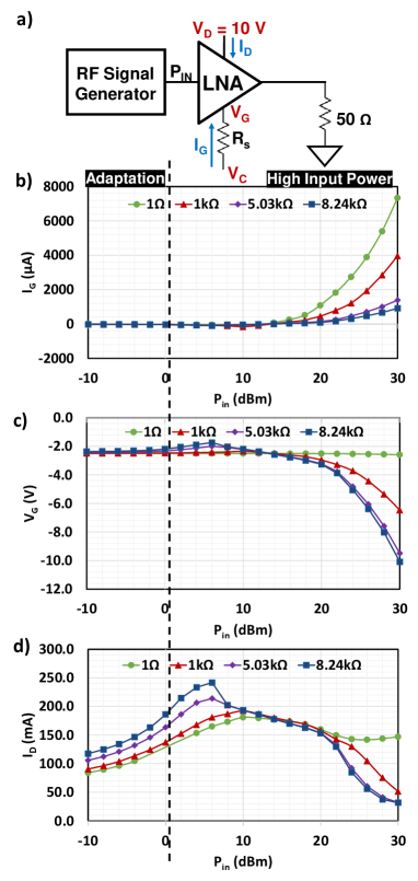
Fig. 6 describes IG, VG and ID vs. different input power with different resistor values in series (RS) at the gate bias of the LNA with the set up in Fig. 6a). The frequency has been set at 2 GHz for the worst-case scenario. As shown in the plots 6b)-d), low power characteristics are very different than the high power characteristics. In the low power region or the adaptation range, IG is actually negative causing VG to tail up due to RS, and with Ohm’s law, when IG is flowing out of the gate, VG is higher than the control voltage (VC). Because of the higher bias in VG, ID is also drawing more current. With increasing in RS, VG tails up higher and ID also reaches a higher point. When the input power transitions to the high power region, IG becomes positive and starts to increase exponentially. As a result of IG becoming more positive, VG starts to drop off exponentially with ID also dropping. With increasing in RS, IG increases more gradually which protects the LNA. Even though VG drops to about -10 V range, it is not significant to cause the LNA to break down. The typical critical value for VDG causing degradation in LNA performance is 30 V, where if VD is 10 V (used in this paper), the minimum VG is -20 V [39].
The characteristics of IG with varying PIN is explained by the Shockley contact at the gate and source of a GaN high-electron-mobility transistor (HEMT). A GaN LNA model can be found in [36]. The Shockley contact is essentially a diode, consequently, at low power levels, the gate experiences a small leakage current; at high power levels, the diode is turned on and IG increases exponentially [40].
Another effect of the GaN LNA is the trapping effect on the gain recovery after a pulse of high input signal [3]. This effect happens much higher than the adaptation range (PIN > 25 dBm), thus during the pulse, the system can be tuned at the maximum possible linearity. When the high input signal is removed, the slow gain recovery does not affect the detection that the input signal is now minimal and returns back to the low power mode.
III-C Bias Control
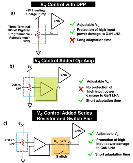
To protect the GaN LNA against the high input power characteristics and provide reasonable adaptation time, the current design for tuning the VG of the LNA is proposed in Fig. 7c). The microcontroller will be configuring the digitally programmable potentiometer (DPP) which is supplied by a -5 V inverting charge pump for the negative VG bias. Following the DPP is a buffer and a parallel structure of a resistor and switch for the control of IG.
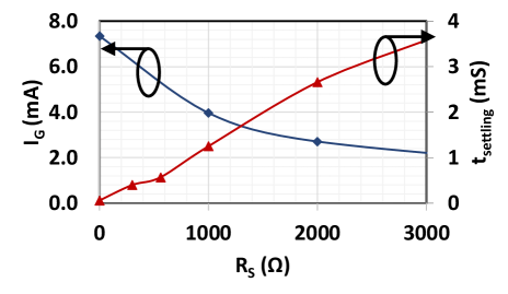
The process for the current design in tuning the VG is shown in Fig. 7. Fig. 7a) considers the case when there is only a DPP connected directly to the gate of the LNA. The drawback of this design is shown in Fig. 8. As the RS to the gate of the LNA increases, the gate current is suppressed but the settling time increases. Since the DPP is in the 100 k range, the high series resistance causes a high RC time constant which increases the settling time (TS) significantly. The increase in Ts would, in turn, increase the adaptation time to tens of milliseconds which is undesirable when one of the goals is to constraint the timing in the millisecond range. To solve the Ts problem, a buffer is added as shown in Fig. 7b) which essentially reduces RS to decrease TS; however, as discussed in Sec. III-B, the reduced RS draws more IG in high power which minimizes the device lifetime.
To balance the IG and Ts trade-off, a parallel resistor-switch pair is added in the current design as shown in Fig. 7c). During the low power and adaptation regions in Fig. 6a), IG is low in the sub-mA region, so the switch can be closed to construct the low resistance path for tuning VG to improve Ts. After the adaptation, the switch will remain closed to maintain a steady bias condition, on the other hand, if the switch opens to place RS in the path, VG would increase as shown in Fig. 7b) and change the bias condition which consumes more power. In the high power region, lower IG is more prominent since VG is set to -2.1 V directly without the adaptation, so TS can be traded for lower IG with the switch being open and resistor in series.
III-D Linearity Decision Making in Incremental Adaptation
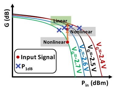
Due to the variable gain behavior of the LNA with changing VG, the ED2 measurements at the output of the LNA are also affected. The gain of the LNA first increases with increasing VG, then decreases after VG-2.5 V in Fig. 4a). Fig. 9 shows that the linear region occurs where the gain of the system remains relatively constant before the 1dB compression point (P1dB) and the nonlinear region occurs where the system is highly compressed beyond P1dB. Even though the gain varies with increasing VG, P1dB monotonically increases with increasing VG. When a high input signal presents in the system at VG=-2.7 V, the signal is highly gain compressed and the system is highly nonlinear. To linearize the system, VG increases in 0.1 V increments. When VG increases from -2.7 V to -2.6 V, the signal becomes less gain compressed but the system remains nonlinear. To further improve the system linearity, VG is increased to -2.5 V. The idea of incrementing VG to improve linearity forms the basis of the incremental adaptation in Sec. IV-A.
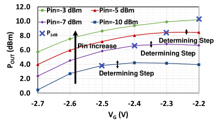
Fig. 10 shows POUT vs VG tuning with respect to different PIN. P1dBs are also shown to show that VG < VP1dB results in a nonlinear system. As PIN increases, the VP1dB also increases. As VG is tuning, the gain of the LNA increases then decreases as shown in Fig. 4a). Due to the effect of LNA gain with different VG and LNA transitioning from non-linear to linear, the determining step decreases with PIN increase. Therefore to accommodate the difference in determining steps in both high and low PIN across different frequencies, a lower determining step is chosen as the linearity threshold which has a drawback of overestimation of VG for lower PIN values. One may suggest that different threshold limits can be used with different PIN values, but this again creates a case-dependent threshold that may not work in other frequencies.
IV Control Mechanisms for Adaptation
IV-A Incremental Adaptation Control Logic
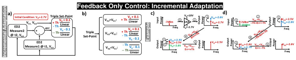
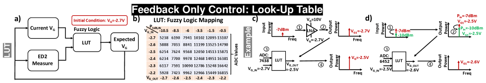
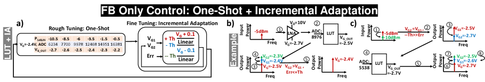
Fig. 11a) describes the control method with incremental adaptation. The LNA is initially in low power mode with VG being initially set at -2.7 V and ED2 will perform the initial measurement at time instance 1 (t1) as the reference. When interference reaches the system, another ED2 measurement at time instance 2 (t2) is taken as the current value. The difference (err) between the current and reference of ED2 is compared with a set of thresholds to start the feedback control. The set of thresholds can be regarded as an extended version of bang-bang control as the triple set-point control in Fig. 11b). The triple set-point has three different conditions: when VG1 at t1 is the same as VG2 at t2, the resulting action is increment VG by 0.1 V if the err is greater than the positive threshold (+Th), decrement VG by 0.1 V if the err is less than the negative threshold (-Th), or maintain the same VG if the err is between +Th and -Th; when VG2 is greater than VG1 (VG is incrementing), the err is compared only to the +Th such that VG incrementes when err is greater than +Th (gain compression observed) or returns to VG1 when err is less than +Th (linear); when VG2 is less than VG1 (VG is decrementing), the err is compared with the -Th and a more negative threshold (–Th) such that VG decrements to find the optimum VG when the err is in between the thresholds (still in the linear region), or returns to VG1 when the err is less than the –Th (gain compression observed). An example of the incremental adaptation is shown in Fig. 11c). When the interference is detected, VG will start incrementing until err is less than the +Th. Another example of when the interference signal changes are shown in 11d). When the interference level decreases, the VG also starts to decrement until err is less than –Th. Note that if the interference level drops a significant amount, VG is back to the initial condition instead of stepping down to start the adaptation.
IV-B Look-Up Table Control Logic
Fig. 12a) describes the control method with a look-up table (LUT). A LUT as shown in Fig. 12b) utilizes the current VG value and the ADC measurement (unit: 10-4 V) of the ED2 at 3 GHz, then outputs the VG value that would bring the LNA back to linearity (High linearity mode). Note that, although not included in the figure, after settling of VG, ED2 is constantly monitored so that if the measurement is within the ADC variation, VG stays at the same value; otherwise, the process starts over with another ED2 measurement. The LUT is generated in a way that for each input power using the P1dB,IN at each VG value and different VG settings, ADC measures at the output of ED2. LUT can be associated with a Fuzzy logic control that unlike the triple set-point control to only have four commands, Fuzzy logic includes a wider range of VG outputs. Each combination input VG and ED2 measurement can be treated as an if-else statement in the Fuzzy logic and returns a preprogrammed output VG [41]. An example of the LUT control is shown in 12c). When the interference is detected, ADC measures at ED2 output. With the ADC measurement of 743.8 mV (ADC reads 7438) and the current VG value of -2.7 V, the LUT determines that a VG value of -2.5 V with a P1dB,IN of -6 dBm is sufficient to bring the system back to linearity. Another example is shown in 12d) in the case of reduced interference level. Again the ADC measurement and current VG value is used to determine that a VG of -2.6 V with a P1dB,IN of -8.5 dBm is sufficient for linearity.
IV-C One-Shot + Incremental Adaptation Control Logic
Fig. 13a) describes the control method with a one-shot for rough tuning and incremental adaptation for fine-tuning. The one-shot is implemented in a LUT style with certain degrees of an underestimate of the output VG value to accommodate different frequencies and different VG values. The incremental adaption again utilizes the triple set-point control with three thresholds and four regions of action. An example is shown in 13b) where when the interference of -5 dBm is detected, one-shot rough tunes the VG to -2.5 V, then the incremental adaptation starts to increment VG for fine-tuning. A second example is shown in 13c) where when the interference level drops significantly, one-shot tunes VG to -2.7 V, and then incremental adaptation steps up to find the optimum VG.
IV-D Comparison of Control Methods
All three methods are intended to control the bias of LNA in order to achieve linearity with a minimum required power consumption from the LNA. LUT has the advantage of being very fast and accurate if the frequency is known so that the specific LUT can be utilized; however, accuracy implies a stringent requirement on the memory space in the microcontroller that multiple LUTs at different frequencies are required. On the other hand, the incremental adaptation only and the one-shot + incremental adaptation methods do not need the frequency information for adaptation as long as the measurement is greater than the interference threshold. However, due to the extra adaptation and the single set linearity threshold, the two methods tend to take longer and are less accurate involving some overestimation of VG. A way to incorporate methods is that when the interference frequency is known, LUT can be used, but when the frequency is unknown, one-shot + incremental adaptation can be used.
IV-E Control Theory for Optimum Bias
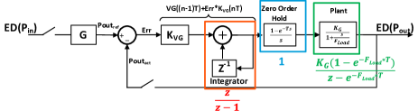
In order to provide a more thorough background on the limitations of the control loop adaptation time, a second-order dynamic system is presented in Fig. 14 following analysis for digital dropout regulators [42, 43]. The control loop models the feedforward and feedback control method with two degrees of observability at the input and output. The model has the following assumptions:
-
1.
flat gain until the P1dB point.
-
2.
gain is not a function of VG and frequency but linearity.
-
3.
VG settling (100kHz) dominates ED bandwidth (40 MHz) and LNA bandwidth.
The goal of the control loop is to minimize the difference between the expected output and the measured output. The expected output is calculated from the measured input and multiplied by a constant LNA gain (G). Both the expected output and the measured output are sampled and subtracted to form an error signal. The error signal multiplies with a proportional constant (KVG) to form a VG that is added to the previous VG through the integrator (). The sampled VG transforms to continuous time through the zero-order hold. Finally, VG supplies to the plant and maps the VG to the measured output. The plant consists of a constant gain KG and a pole from the VG settling time (FLoad) with a z-domain equation of . Ts is the ADC sampling period(we will approximate to 50s for simpler demonstration of calculation). The open loop gain is
| (1) |
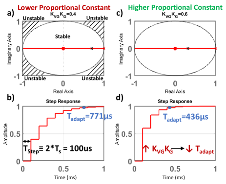
To maximally match the existing control methods, since each adaptation step requires two samples of measurement to ensure accuracy which will be explained shortly, 2*Ts=100 s with a sampling frequency Fs/2=10 kHz is used. With FLoad=100 kHz, Fs < FLoad, Fs dominants in the settling time. From Fig. 15a)-b), the proportional constant is low with KVGKG=0.4, the total settling time or the adaptation time is 771 s. From Fig. 15c)-d), KVGKG=0.6, the total settling time is 436 s. As shown in the step response, because TLoad < Ts, each step takes 2*Ts. The different proportional constant can be thought of as the one-shot values in the one-shot + incremental adaptation method, with a higher one-shot value (high KVGKG), the number of steps to reach a steady state is lower, hence a faster response.
Overall, the adaptation time can be approximated as
| (2) |
where
| (3) |
In the equations, N is the number of steps which is a function of the proportion constant, Ts is the ADC sampling time, Tprocess is the processing time for the microcontroller to make decisions, TVG is the VG tuning time, TLNA is the propagation time from tuned VG to the settling of the LNA and TED is the propagation time from settled LNA output to settled ED output. Note that the first sample of the ADC contains some of the transient response which lacks accuracy, so the second sample is taken to be the accurate one to the processing, hence the 2*Ts in Eq.2. In order for the second sample to be accurate, the first sample of the ADC should contain all of the transient responses, hence Eq.3 shows that the sampling time of the ADC needs to be greater than the total propagation and settling time for each component.
Some known timing characteristics are:
-
•
TVG 4 - 10 s per step depending on the step size
-
•
Tprocess is negligible in the ranges of <s
-
•
Ts2 s - 1 ms or Fs1 - 500 kHz
-
•
TLoad TVG4 - 10 s or FLoad FVG100 - 250 kHz.
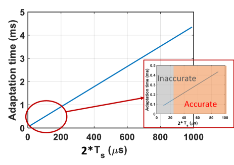
Since highest Fs is 500 kHz, Fs << FLoad, a linear increase of adaptation time vs. ADC sampling time is observed in Fig. 16, assuming TVG 10s and a negligible processing time with KVGKG=0.6. Note that in the figure, a sufficient margin higher than TVG ( >25us of total ADC measurement time for 2 samples) is needed for an accurate reading. The simulations in Fig. 16 allow for a more accurate estimation of the minimum adaptation time for the control loop. The adaptation time is strongly dependent on the ADC sampling rate, so if ADC sampling rate can be increased, the adaptation time can be reduced. Otherwise, the minimum adaption time is about 150 s with the current sampling rate with the number of steps to settling being approximately four.
V Measurement Results
V-A Results from Feedback Only Control
| Control | Interference On Off | Interference Level Change |
|---|---|---|
| Incremental Adaptation | -Slowest adaptation time (600 s) -wider frequency range adaptation | -skips steps during interference level change -settles to different VG |
| Look-Up Table | -Fastest adaptation time (180 s) -all steps are visible during interference level change -narrower frequency range adaptation -requires more memory space to implement full look-up table | -all steps are visible during interference level change -settles to the same VG most of the time |
| One-Shot + Incremental Adaptation | -Faster adaptation time (450 s) -wider frequency range adaptation -frequency specific one-shot or underestimation during one-shot | -skips steps during interference level change -frequency specific one-shot or underestimation during one-shot |
Feedback-only control implements a temporal control where the tuning uses two samples of the output signal levels at different times. The results are summarized in Table II.
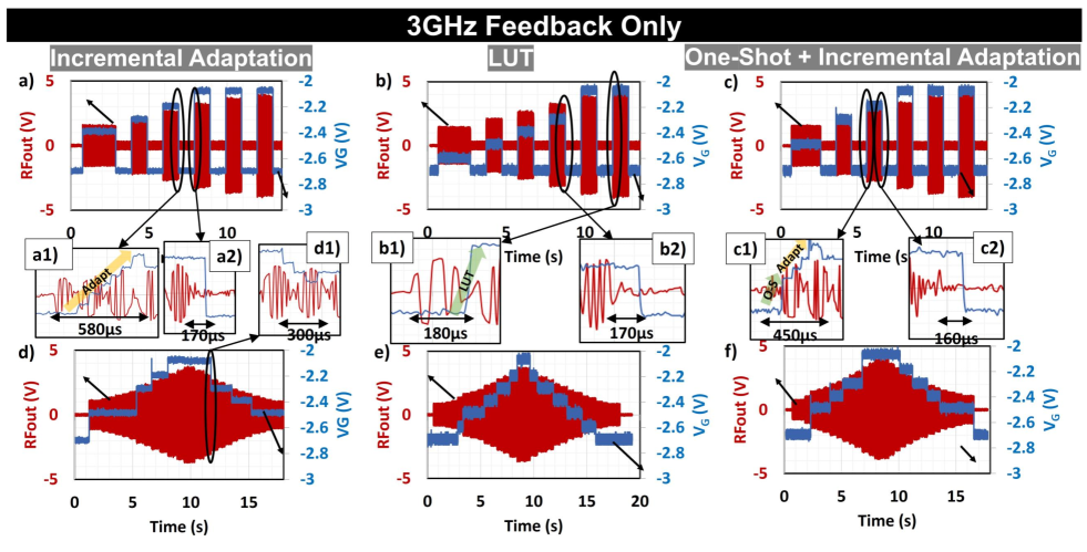
Fig. 18 presents the adaptation and timing characteristics for different control methods with the measurement setup in Fig. 17. Note that after zooming into the transient, the RF output measured using an oscilloscope is not a perfect sine wave due to the undersampling of the oscilloscope trying to capture the signal with a larger time scale. Fig. 18a) - c) show the adaptation of the LNA by varying different interference levels on and off. Different high interference levels at 3 GHz are forced at the input with the expectation of VG to increase from -2.6 V to -2.1 V in the increment of 0.1 V; at low interference levels, VG is expected to drop down to -2.7 V. A summary of different settled VG with respect to different input interference levels is presented in Fig. 19a). As expected, the LUT(Fig. 18b) is more aligned with the expected VG as the LUT values are specifically for 3 GHz while both the incremental adaptation only(Fig. 18a) and the one-shot + incremental adaptation(Fig. 18c) overestimates VG. Fig. 18a1), b1) and c1) show the tuning times to adapt to an interference level for the incremental adaptation, LUT and one-shot + incremental adaptation are 580, 180 and 450 s respectively. Fig. 18a2), b2) and c2) show the tuning times to adapt to a disappearing interference for the three control methods are very similar, around 170 s. Fig. Fig. 18d) - f) show the adaptation of the LNA when the interference level increases from -12.5 dBm to -0.5 dBm and backs down to -12.5 dBm in increments of 1 dBm. With the LUT method in Fig. 18e), every step of VG is shown and roughly the same settling VG for the same interference level, whereas for the incremental adaptation (Fig. 18d) and one-shot + incremental adaptation method(Fig. 18f), some VG steps are skipped and sometimes different VG values for the same interference level. Fig. 18d1) shows that when the interference level decreases, the control loop is able to step down and adapt.
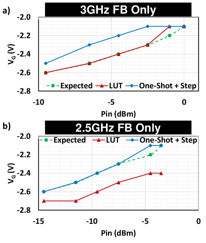
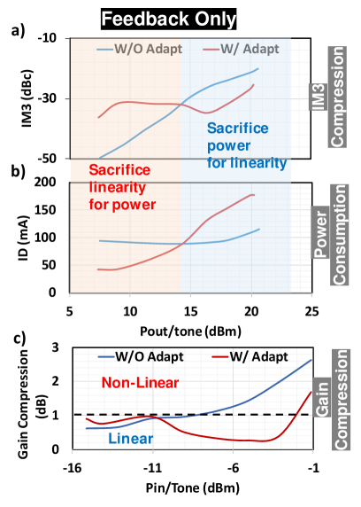
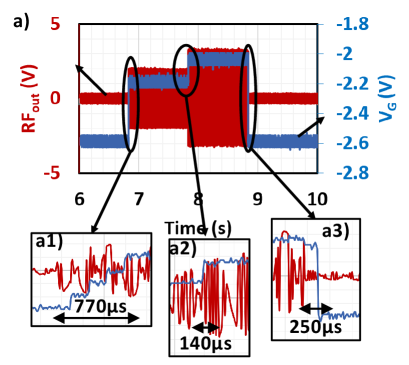
Fig. 19 shows the settling VG values for different methods of control vs. input power with frequencies of 3 GHz and 2.5 GHz. In the 3 GHz plot in Fig. 19a), LUT method almost matches up with all the expected VG to bring the LNA back to linearity whereas the incremental adaptation only and one-shot + incremental adaptation overestimates for many PIN values. However, in the 2.5 GHz plot in Fig. 19b), LUT significantly underestimates the necessary VG for linearity due to the LUT is only captured at 3 GHz and the algorithm tries to match the 2.5 GHz ADC values with the 3 GHz values. On the contrary, the one-shot + incremental adaptation method matches up with the expected better at 2.5 GHz than at 3 GHz due to the set threshold value being better suited at 2.5 GHz since the threshold value is chosen to adapt to a wider range of frequencies.
Fig. 20 shows the trade-offs between an adaptive system vs. a non-adaptive system operating in nominal conditions with a two-tone measurement. Fig. 20a) and b) show that when the interference is low, the adaptive system consumes less power while still maintaining linearity for the LNA in comparison to the non-adaptive system having a higher IM3 compression and consumes more power; when the interference is high, the adaptive system consumes more power to bring the LNA back to linearity with a higher IM3 compression compared to the non-adaptive system with lower IM3 compression (LNA is non-linear) and lower power consumption. Fig. 20c) shows that the adaptive system is able to keep the LNA in the linearity range over a wider input range than the non-adaptive system in the nominal condition.
V-B Results from Feedforward + Feedback Control
Feedforward + feedback design allows a spacial control of the system where both the input and output signal levels can be sampled, and the linearity is determined by comparing the measured gain with the expected gain to ensure no gain compression. Fig. 21 shows that the tuning circuit is able to use spatial control to tune the VG of the LNA as the interferences appear, increase and disappear; however, this method also suffers from an overestimation of the VG value that a higher VG value is determined. Note from Fig. 21a1), unlike the overshoot in the feedback only incremental adaptation control, since this board has the extra degree of observability and that the measured gain is directly compared with the expected gain, tuning does not give overshoot in VG. From Fig. 21a1-3), the tuning times for the interference appearance, increasing of interference, and disappearance of interference are 770 s, 140 s and 250 s respectively. The tuning times are below 1 ms; however, as shown in Fig. 21a1), a longer tuning time is needed than the feedback only incremental adaptation control due to ADC sampling time is lengthened to accurately measure the input power being close to the sensitivity level.
V-C System Comparison
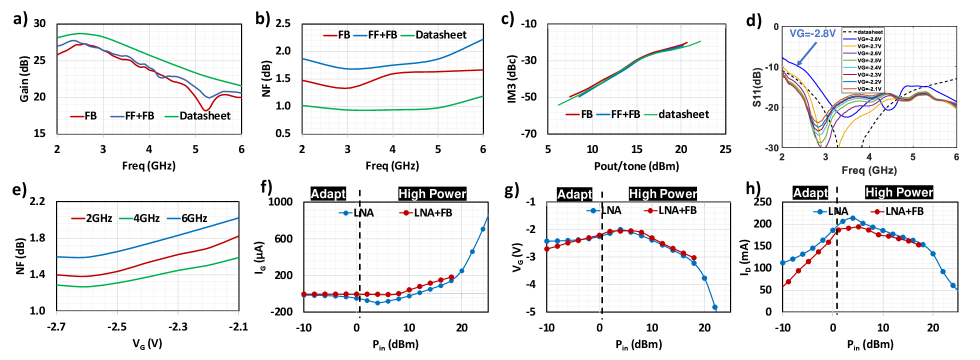
Fig. 22 presents different LNA characteristics after implementation on the feedback-only board and the combined feedforward and feedback board with the datasheet values in similar bias conditions of VD = 10 V and ID 100 mA. Note that the datasheet values are measured directly on the die, by implementing on a PCB, some degree of degradation in the gain and NF are expected. Fig. 22a) shows the gain comparison over the frequency range of 2-6 GHz. The gain of the boards shows a few dB of degradation in comparison to the datasheet while little difference between the different boards. Fig. 22b) shows the noise figure (NF) vs. frequency for different boards. The feedback-only board has an NF about 0.5 dB higher than the datasheet, and as expected with the feedforward and feedback combined board, the NF is again about 0.3 dB higher than the feedback-only layout due to the extra directional coupler before the LNA. Fig. 22c) shows the 3rd order intermodular product (IM3) compression vs. desired output power for each tone. The IM3 compression are relatively close across different boards and the datasheet.
Fig. 22d) shows different return loss (S11) with respect to different VG values. As shown in the plot, when VG=-2.8 V, the return loss is worse than all of the other voltages, so when implementing the control loop, only VG greater than -2.8 V is considered. For VG between -2.7 V to -2.1 V, the majority of the responses have an S11 lower than -15 dBm, other parts have an S11 lower than -10 dBm. Fig. 22e) shows NF across VG tuning range for 2, 4 and 6 GHz. Across VG the NF can increase about 0.4 dB. When interference is low, instead of operating at nominal VG of -2.4 V with a higher NF, lower NF can be achieved in the adaptive system with VG of -2.7 V. When interference is high, higher linearity is achieved with higher NF and power consumption.
Fig. 22f)-h) shows the comparison of the high power data for the LNA in Fig. 6 and LNA in a feedback system. In the adaptation range, the VG in the feedback system is continuously increasing to maintain linearity by adapting to the current input while the VG increase in the LNA only system is caused by the non-linearity of the LNA. The difference in linearity in the two systems can also be observed in the IG, where the linear system has a consistent IG in the ranges of A whereas the non-linear system sees more of a revered biased current. ID for both systems show an increase because of the increase in VG. In the high power range, the currents and the voltages are starting to overlap showing similar high power effects as described in Sec. III-B.
Table III shows comparisons between the datasheet LNA in nominal condition, LNA with feedback control and LNA with feedback + feedforward control. According to the datasheet [28], the GaN LNA’s nominal condition is VD=10 V and ID=100 mA, which consumes about 1 W of power. The controls consume 10 of total LNA nominal power for a better linearity and LNA power consumption trade-off. Most of the control power derives from the microcontroller consuming 80 mW of power, which is about 80-90 of total control power. LNA with control gives a wide tuning range in power and linearity. When the system is operating in low-power mode in a large EW receiver array, the power saving can be significant. Extra system power is consumed when higher linearity is required to decode the signal.
| Specs | LNA | LNA+FB | LNA+FB+FF |
|---|---|---|---|
| Gain (dB)∗ | 28 | 26.5 | 26.5 |
| NF (dB)∗ | 1 | 1.4 | 1.7 |
| P1dB,IN (dBm) | -7 | -10.5 0.5 | -14 0.5 |
| LNA Power (W) | 1 | 0.5 2 | 0.3 1.8 |
| Control Power (W) | 0 | 0.09 | 0.1 |
| Observation Points | 0 | 1 | 2 |
| Control Method | none | Temporal | Spacial |
| Tuning Step (us) | none | 85 | 150 |
∗ 3 GHz Data
Feedforward + feedback design includes two pairs of directional coupler and ED. With the extra directional coupler and ED1 before the LNA, NF increases by 0.3 dB, and overall control power consumption increases by another 10 mW than feedback only design; however, the design gives more information on the input signal that will be more relevant in future works of an adaptive receiver. For example, if a filter was placed to remove the interference signal, the extra information on the input signal would allow us to determine if the interference is still present or has already been removed by the filter. The feedback-only design provides a simpler solution for the current application to detect the presence and the level of interference signal at the output of the LNA. Contrary to the spacial control in the feedforward + feedback design, feedback-only design implements a temporal control. At the current stage, the extra degree of observability at the input of the LNA is not needed as no filter is present.
![[Uncaptioned image]](https://cdn.awesomepapers.org/papers/4e06baa1-2107-48d6-8dcb-839ea6870100/x23.png)
∗ IC+COTS: Custom IC with COTS connected through SMA connector. COTS: COTS connected through SMA connector. COTS+PCB: some custom microwave components connected with some components integrated into the PCB. Integrated PCB: components are integrated into one PCB without any SMA connections to other components.
V-D Comparison Table
Table IV shows the different works that contribute to adaptive transceivers over different implementation methods for higher resilience towards undesired interference.
VI Future Work
The current work can be further extended by implementing a complete RF receiver front end, adding interference frequency detection and/or interference filtering circuitry for interference compression, and better use of some frequency-dependent control methods. The interference frequency detection circuits can assist with deciding other signals for interference cases such as strong signal and strong interference. The adaptation time as well as the power consumption of the controlling circuit can be further minimized. If Apollo4 microcontroller is utilized, the microcontroller would only consume mW’s of power and reduced the total control power to <3 of nominal LNA power consumption [44]. A different LNA with orthogonal tunability can be explored so that with a blocker, the gain can also be tuned to achieve large signal linearity. Noise figure of the front end can also be further improved.
The concept of the work can be expanded into other technologies by having a strong correlation between the bias voltages of the LNA and linearity and the accessibility of the bias voltages. The work can also be expanded into other frequencies with correct characterizations of different components. The LNA and the onboard directional couplers are specifically for 2-6 GHz, and the envelope detector 2 can function up to 43.5 GHz.
If similar systems were to be built in low-power receivers, a custom ASIC design can bring down the control loop power by orders of magnitude. Such systems are part of future work and will expand the applicability of instinctual receivers to much wider power categories of RF systems.
VII Conclusion
This paper presents the first instinctual GaN LNA system demonstration with intelligent localized sensing, processing, and feedback controls to achieve sub-1ms adaptation to a variety of interference scenarios. GaN LNA is utilized for the high power handling capabilities in radar and EW applications. The system consumes 10 of nominal LNA power to provide a wide range of tuning. The linearity tuning range is about 11 dB; LNA power consumption tuning range is about 0.5-2 W; NF changes about 0.4 dB across the tuning range. When the frequency is known using LUT, the system adapts to an interference very accurately to bring the LNA back to linearity. When the frequency is unknown, the system is still able to adapt to interference with extra power consumption using either incremental adaptation only or one-shot + incremental adaptation. The feedback-only board provides simplicity of the design for this application. The adaptation time for the system is <1 ms which closely matches the theoretical simulations.
References
- [1] J. Yang, B. Chatterjee, M. Thorsell, M. Kowalewski, B. Edward, D. Peroulis, and S. Sen, “Instinctual interference-adaptive low-power receiver with combined feedforward and feedback control,” IEEE Microwave and Wireless Components Letters, vol. 31, no. 6, pp. 771–774, 2021.
- [2] Y. Adediran, H. Lasisi, and O. Okedere, “Interference management techniques in cellular networks: A review,” Cogent Engineering, vol. 4, no. 1, p. 1294133, 2017. [Online]. Available: https://doi.org/10.1080/23311916.2017.1294133
- [3] O. Axelsson, N. Billström, N. Rorsman, and M. Thorsell, “Impact of trapping effects on the recovery time of gan based low noise amplifiers,” IEEE Microwave and Wireless Components Letters, vol. 26, no. 1, pp. 31–33, 2016.
- [4] H. Li, X. Yang, and C. E. Saavedra, “A feedforward linearization technique implemented in if band for active down-conversion mixers,” in 2017 IEEE Radio Frequency Integrated Circuits Symposium (RFIC), 2017, pp. 296–299.
- [5] T. Nesimoglu, Z. Charalampopoulos, and M. A. Beach, “Interference suppression in radio receivers by using frequency retranslation,” in 2009 IEEE 10th Annual Wireless and Microwave Technology Conference, 2009, pp. 1–5.
- [6] T. Nesimoglu, M. Beach, J. MacLeod, and P. Warr, “Mixer linearisation for software defined radio applications,” in Proceedings IEEE 56th Vehicular Technology Conference, vol. 1, 2002, pp. 534–538 vol.1.
- [7] M. Parvizi, K. Allidina, and M. N. El-Gamal, “An ultra-low-power wideband inductorless cmos lna with tunable active shunt-feedback,” IEEE Transactions on Microwave Theory and Techniques, vol. 64, no. 6, pp. 1843–1853, 2016.
- [8] A. Dehqan, E. Kargaran, K. Mafinezhad, and H. Nabovati, “An ultra low voltage ultra low power cmos uwb lna using forward body biasing,” in 2012 IEEE 55th International Midwest Symposium on Circuits and Systems (MWSCAS), 2012, pp. 266–269.
- [9] C. J. Jeong, W. Qu, Y. Sun, D. Y. Yoon, S. K. Han, and S. G. Lee, “A 1.5v, 140µa cmos ultra-low power common-gate lna,” in 2011 IEEE Radio Frequency Integrated Circuits Symposium, 2011, pp. 1–4.
- [10] S. N. Ali, M. Aminul Hoque, S. Gopal, M. Chahardori, M. A. Mokri, and D. Heo, “A continually-stepped variable-gain lna in 65-nm cmos enabled by a tunable-transformer for mm-wave 5g communications,” in 2019 IEEE MTT-S International Microwave Symposium (IMS), 2019, pp. 926–929.
- [11] Z. Hao, L. Zhiqun, and W. Zhigong, “A wideband variable gain differential cmos lna for multi-standard wireless lan,” in 2008 International Conference on Microwave and Millimeter Wave Technology, vol. 3, 2008, pp. 1334–1337.
- [12] S. Popuri, V. S. R. Pasupureddi, and J. Sturm, “A tunable gain and tunable band active balun lna for ieee 802.11ac wlan receivers,” in ESSCIRC Conference 2016: 42nd European Solid-State Circuits Conference, 2016, pp. 185–188.
- [13] S. N. Ali, M. Aminul Hoque, S. Gopal, M. Chahardori, M. A. Mokri, and D. Heo, “A continually-stepped variable-gain lna in 65-nm cmos enabled by a tunable-transformer for mm-wave 5g communications,” in 2019 IEEE MTT-S International Microwave Symposium (IMS), 2019, pp. 926–929.
- [14] S. Sen, M. Verhelst, and A. Chatterjee, “Orthogonally tunable inductorless rf lna for adaptive wireless systems,” in 2011 IEEE International Symposium of Circuits and Systems (ISCAS), 2011, pp. 285–288.
- [15] J.-Y. Hsieh and K.-Y. Lin, “A 0.6-v low-power variable-gain lna in 0.18- m cmos technology,” IEEE Transactions on Circuits and Systems II: Express Briefs, vol. 67, no. 1, pp. 23–26, 2020.
- [16] L. Hanning, J. Bremer, M. Ström, N. Billström, T. Eriksson, and M. Thorsell, “Optimizing the signal-to-noise and distortion ratio of a gan lna using dynamic bias,” in 2018 91st ARFTG Microwave Measurement Conference (ARFTG), 2018, pp. 1–4.
- [17] D. Banerjee, S. K. Devarakond, X. Wang, S. Sen, and A. Chatterjee, “Real-time use-aware adaptive rf transceiver systems for energy efficiency under ber constraints,” IEEE Transactions on Computer-Aided Design of Integrated Circuits and Systems, vol. 34, no. 8, pp. 1209–1222, 2015.
- [18] R. Senguttuvan, S. Sen, and A. Chatterjee, “Vizor: Virtually zero margin adaptive rf for ultra low power wireless communication,” in 2007 25th International Conference on Computer Design, 2007, pp. 580–586.
- [19] S. Sen, V. Natarajan, R. Senguttuvan, and A. Chatterjee, “Pro-vizor: Process tunable virtually zero margin low power adaptive rf for wireless systems,” in 2008 45th ACM/IEEE Design Automation Conference, 2008, pp. 492–497.
- [20] N. Cao, B. Chatterjee, J. Liu, B. Cheng, M. Gong, M. Chang, S. Sen, and A. Raychowdhury, “A 65 nm wireless image soc supporting on-chip dnn optimization and real-time computation-communication trade-off via actor-critical neuro-controller,” IEEE Journal of Solid-State Circuits, vol. 57, no. 8, pp. 2545–2559, 2022.
- [21] Y. Xu, J. Zhu, and P. R. Kinget, “A blocker-tolerant rf front end with harmonic-rejecting -path filter,” IEEE Journal of Solid-State Circuits, vol. 53, no. 2, pp. 327–339, 2018.
- [22] D. Lee and K. Kwon, “Cmos channel-selection lna with a feedforward n-path filter and calibrated blocker cancellation path for fem-less cellular transceivers,” IEEE Transactions on Microwave Theory and Techniques, vol. 70, no. 3, pp. 1810–1820, 2022.
- [23] M. Meghdadi and M. Sharif Bakhtiar, “Two-dimensional multi-parameter adaptation of noise, linearity, and power consumption in wireless receivers,” IEEE Transactions on Circuits and Systems I: Regular Papers, vol. 61, no. 8, pp. 2433–2443, 2014.
- [24] S. Sen, D. Banerjee, M. Verhelst, and A. Chatterjee, “A power-scalable channel-adaptive wireless receiver based on built-in orthogonally tunable lna,” IEEE Transactions on Circuits and Systems I: Regular Papers, vol. 59, no. 5, pp. 946–957, 2012.
- [25] S. Sen, V. Natarajan, S. Devarakond, and A. Chatterjee, “Process-variation tolerant channel-adaptive virtually zero-margin low-power wireless receiver systems,” IEEE Transactions on Computer-Aided Design of Integrated Circuits and Systems, vol. 33, no. 12, pp. 1764–1777, 2014.
- [26] S. Sen, R. Senguttuvan, and A. Chatterjee, “Environment-adaptive concurrent companding and bias control for efficient power-amplifier operation,” IEEE Transactions on Circuits and Systems I: Regular Papers, vol. 58, no. 3, pp. 607–618, 2011.
- [27] M. Abu Khater and D. Peroulis, “Multi-octave interference detectors with sub-microsecond response,” 2022. [Online]. Available: https://arxiv.org/abs/2207.00937
- [28] Qorvo. (2020) TGA2611-SM. [Online]. Available: https://www.qorvo.com/products/p/TGA2611-SM
- [29] T. Instruments. (2020) LMH2120. [Online]. Available: https://www.ti.com/product/LMH2120
- [30] Analog-Devices. (2020) ADL6010. [Online]. Available: https://www.analog.com/en/products/adl6010.html
- [31] ——. (2020) LTC1983. [Online]. Available: https://www.analog.com/en/products/ltc1983.html
- [32] ——. (2020) AD5260. [Online]. Available: https://www.analog.com/en/products/ad5260.html
- [33] ——. (2020) LTC6255. [Online]. Available: https://www.analog.com/en/products/ltc6255.html
- [34] ——. (2020) ADG601. [Online]. Available: https://www.analog.com/en/products/adg601.html
- [35] NXP. (2021) LPC55S69-EVK: LPCXpresso55S69 Development Board. [Online]. Available: https://www.nxp.com/design/development-boards/lpcxpresso-boards
- [36] Y. Chen, R. Coffie, W.-B. Luo, M. Wojtowicz, I. Smorchkova, B. Heying, Y.-M. Kim, M. V. Aust, and A. Oki, “Survivability of algan/gan hemt,” in 2007 IEEE/MTT-S International Microwave Symposium, 2007, pp. 307–310.
- [37] G. Sanna, G. Montisci, Z. Jin, A. Fanti, and G. A. Casula, “Design of a low-cost microstrip directional coupler with high coupling for a motion detection sensor,” Electronics, vol. 7, no. 2, 2018. [Online]. Available: https://www.mdpi.com/2079-9292/7/2/25
- [38] M. Rudolph, R. Behtash, R. Doerner, K. Hirche, J. Wurfl, W. Heinrich, and G. Trankle, “Analysis of the survivability of gan low-noise amplifiers,” IEEE Transactions on Microwave Theory and Techniques, vol. 55, no. 1, pp. 37–43, 2007.
- [39] J. Joh, L. Xia, and J. A. del Alamo, “Gate current degradation mechanisms of gan high electron mobility transistors,” in 2007 IEEE International Electron Devices Meeting, 2007, pp. 385–388.
- [40] O. Axelsson, M. Thorsell, K. Andersson, and N. Rorsman, “The effect of forward gate bias stress on the noise performance of mesa isolated gan hemts,” IEEE Transactions on Device and Materials Reliability, vol. 15, no. 1, pp. 40–46, 2015.
- [41] W. Dwiono, A. J. Taufiq, and W. Winarso, “Simple implementation of fuzzy controller for low cost microcontroller,” in 2019 International Conference of Artificial Intelligence and Information Technology (ICAIIT), 2019, pp. 26–30.
- [42] S. B. Nasir, S. Gangopadhyay, and A. Raychowdhury, “All-digital low-dropout regulator with adaptive control and reduced dynamic stability for digital load circuits,” IEEE Transactions on Power Electronics, vol. 31, no. 12, pp. 8293–8302, 2016.
- [43] S. Gangopadhyay, Y. Lee, S. B. Nasir, and A. Raychowdhury, “Modeling and analysis of digital linear dropout regulators with adaptive control for high efficiency under wide dynamic range digital loads,” in 2014 Design, Automation Test in Europe Conference Exhibition (DATE), 2014, pp. 1–6.
- [44] Ambiq. (2022) Apollo4. [Online]. Available: https://ambiq.com/apollo4/