Inconsistencies between experimental and theoretical band structure of TiSe2
Abstract
Renew interest in the charge density wave phase of TiSe2 stems from the realization of its unique driving mechanism, the so called excitonic insulator phase. Existing claims are motivated by model calculations of the band structure. In this study, angle resolved photoemsision spectroscopy and density functional theory for TiSe2 are directly compared. The substantial discrepancies found between the two descriptions cast serious doubts on the exitonic insulator scenario as the correct physical mechanism underlying the periodic lattice distortion at low temperature. In particular, the formation of a valence-conduction hybridization gap in the bulk band structure is not present in the experimental data. Therefore, the origin of the structural transition in TiSe2 cannot be fully explained within the existing theoretical models.
Charge density wave (CDW) is an intriguing second order phase transition, usually occurring in low dimensional systems [1, 2]. Below a critical temperature, the lattice experience a periodic distortion accompained by the opening of gaps at specific points of the Fermi surface (nesting sites), lowering the system energy [1, 2]. Among the many materials, CDW is most frequently studied in transition metal dichalcogenides (TMDCs). TiSe2 is a case in point, having gained particular attention due to emergent superconductivity with Cu doping or under pressure [3, 4]. It undergoes a structural transition at 200 K with a formation of a 2a 2a 2c periodic lattice distortion [5, 6]. However, unlike in other TMDC materials, the phase transition in TiSe2 cannot be explained within the ordinary nesting scenario since the Fermi surface is claimed to have no parallel portions [7, 8].
Although identifying the mechanism responsible to stabilize the distorted phase has been the subject of many studies, representing decades of cumulative efforts, the topic still remains elusive and controversial. So far, three main scenarios have been proposed. First is the excitonic insulator model as a purely electronic interaction [8, 9, 10]. In this model, the CDW is driven by the poorly screened Coulomb interactions between electrons and holes. A second model attributes to the electron-phonon coupling the origin of the CDW instability, which is eventually resolved via Peirls or Jahn-Teller type of mechanisms[11]. Finally, in the third model, the combined effect of electron-hole and electron-phonon coupling is responsible for the transition [12].
In this context, the excitonic insulator phase has received the greatest attention [13, 14, 15, 16, 9]. The identification of an emergent bulk band gap with a characteristic band dispersion in the distorted phase is a key element of this model. Therefore, angle resolved photoemission spectroscopy (ARPES) is the experimental tool of choice to verify this model. The prediction is based on the large overlap ( 0.55 eV) between valence and conduction bands at the and points, respectively, found in the calculated band structure for the normal phase of TiSe2.[9, 17, 18, 19, 20, 21, 22]. Upon a periodic lattice distortion, these two high symmetry points become equivalent with consequent folding of the bands. The resulting band degeneracy close to the Fermi level would then be resolved by opening an hybridization gap, thereby leading to the realization of the excitonic insulator material.
However, the predicted bands overlap is not born out by the experimental band structure of TiSe2, which shows an indirect bulk band gap between valence band maximum and conduction band minimum in the normal phase [23, 24, 25, 22]. This would prevent band hybridization in the distorted phase which is the essential mechanism for the exciton insulator phase to emerge. But the gap is smaller than 50 meV, and therefore it is assumed that the overall predictions will not be affected [7]. In principle, one could speculate on a temperature induced band shift to close the gap. However conduction and valence band are found experimentally to shift rigidly in the same direction as a function of temperature [10]. Therefore, conduction and valence band overlapping is extremely unlikely to occur and with it the band hybridization in the distorted phase.
Furthermore, our recent ARPES study shows that the experimental spectra are compatible with a gapless surface electronic structure of TiSe2 [26]. In the same work, the earlier ARPES results are largely reproduced and new results are added, showing that the observation of a bulk band gap is based on undefined features in the ARPES spectra and is therefore dubious. Therefore, inconsistencies between the experimental and theoretical band structure remain elusive and lead to inconclusive interpretations of the experimental data. These issues are critical to understand the nature of the structural transition in TiSe2.
Here, we present a combined photoemssion and density functional theory (DFT) study of the band structure of TiSe2. The predicted and measured dispersion of the bands differs significantly. In particular, it is impossible to fit simultaneously the positions of valence and conduction bands. The expected band hybridization between conduction and valance band is absent in the experimental data. Furthermore, the surface electronic structure is found gapless in the distorted phase, directly ruling out the exitonic insulator scenario. Surprisingly, only the Fermi surface nesting remains as possible mechanism for the CDW transition.
ARPES experiments were performed at the 21ID-I ESM beamline at the National Synchrotron Light Source II (NSLS-II), using a DA30 Scienta electron spectrometer with an energy resolution better than 15 meV. The analyzer slit was along to the - - direction of the hexagonal Brillouin zone. The electric field with linear vertical (LV) polarized light was parallel to the sample surface and analyzer slit while laying in the incident plane for linear horizontal (LH) polarized light. Band structure calculations were performed with the Quantum Espresso (QE) package, based on density functional theory [27, 28]. Crystal structure for the distorted phase was adopted from Ref. 6. Samples were obtained from 2dsemicondcutors.
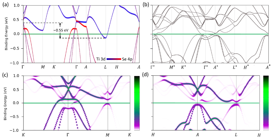
The orbital projected band structure for the normal phase is given in Figure 1(a). Spectral contribution to the valence band around the ()-point is dominated by the Se-4p and the conduction band is contributed mostly by V-3d atomic orbitals. The Fermi level crosses the bottom of the conduction band at point while the tip of the valence band sits 0.46 eV above the predicted Fermi level. This leads to have a 0.55 eV overlapping between two bands as marked with dashed horizontal lines in Figure 1(a).
The folded electronic structure in the 2 2 2 distorted phase presents a strong overlap between the valence and conduction bands inducing a - band hybridization at the Fermi level (Figure 1(b)). In detail, an energy gap opens at the -point while the band structure remains gapless at the -point due to the orbital selective kz dispersion of the valence band [22]. Furthermore, as shown in the unfolded band structure, the valence band tip flattens (Figure 1(c-d)). This modification in the electronic structure is widely regarded as the characteristic signature of the exitonic insulator state, manifesting through the formation of the back-folded valence and conduction bands [13, 14, 15, 16, 9].
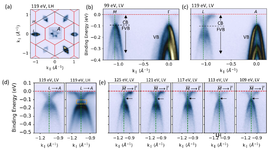
We next discuss the experimental band structure in Figure 2, and 3. A well defined Fermi surface is observed at the -plane. It consists of ellipsoidal pockets located at -point and a star shaped dispersion in the zone center (Figure 2(a)). The periodic lattice distortion is confirmed through the observation of folded valence bands at the and -points in the ARPES spectra (Figure 2(b-c)). In contrast to the expected bulk gap resulting from the - hybridization, clear gapless surface electronic structure is observed with a overlap at 100 meV below the Fermi level (Figure 2(d)). With linear horizontal line the situation is less clear, due to the higher intensity of a second, lower lying, valence band. The resulting intensity decrease just above this band can give the appearance of the opening of a gap between valence and conduction in the region marked by the yellow box. Furthermore, the band overlap displays a 2D nature as shown in the photon energy dependent data (Figure 2(e)). This behavior renders unlikely a kz dependent bulk band gap scenario as proposed in previous studies [22, 24].
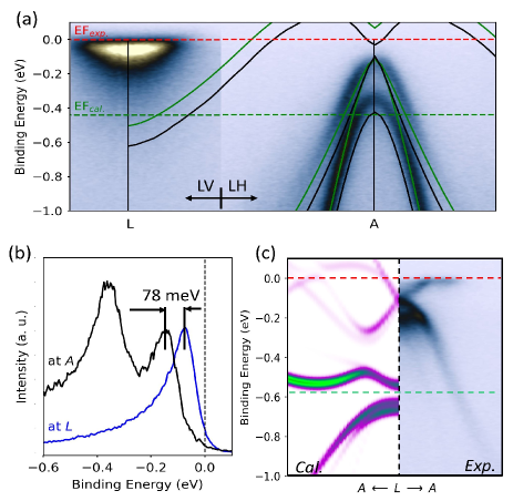
Experimental and computed band structures are compared in Figure 3 to disclose inconsistencies and find the origin of the gapless surface electronic structure. The energy scales are aligned at the top of the valence band at -point (Figure 3(a)). Note that in this case there is a large mismatch between theory and experiment at the -point. At variance with the large overlap predicted for the - states, the experimental band structure in the normal state exhibits a 78 meV indirect gap between conduction and valence bands (Figure 3(a-b)) as consistent with previous reports [22, 24, 23]. Thereby, the band folding in the distorted phase is not expected to induce an hybridization gap. A similar type of intractable inconsistency is found in the distorted phase. Persisting with the same energy scale alignment, one achieves a nice matching of bands close to the Fermi level at the expense of a complete failure at higher binding energies.
As shown above, calculated and experimental band structures are essentially consistent in the literature but differ considerably between themselves. In this situation to compare them, either the binding energy of the conduction band bottom or the tip of valence band needs to be taken as a reference. A criterion must be determined in order to decide which one is more relevant to the experimental data. In previous studies where the conduction band bottom is aligned, a prominent inconsistency for the rest of the band structure is evident [21, 29]. Specifically, the major issue is that the valence band tip falls far above the Fermi level. Then, the indirect bulk band gap in the normal phase becomes inaccessible in ARPES while it is experimentally claimed to be persistent across the structural transition [22, 24, 23]. However in all experimental works, it is well established that the valence band is located below the Fermi level. Therefore, it seems more safe to take the binding energy of the valence band as a reference point to match the computed band structures.
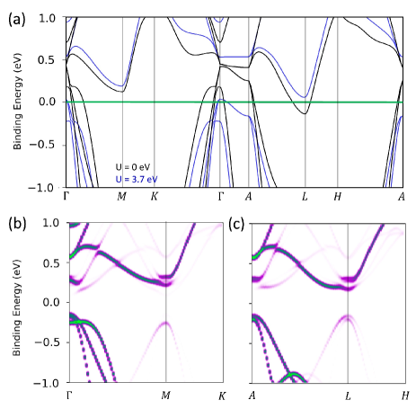
The essential mismatch between measured and calculated band structure is known in the literature. But it is usually ignored when the experimental data are analyzed [22, 7, 21, 30]. A few studies address the issue by incorporating an Hubbard U term and a quasi-self-consistent G0W0 approach [21, 30]. However, the beneficial effects of these methods in reproducing some aspect of the band structure are voided by the new problems that they bring in. We reproduce a similar band structure calculation using an Hubbard U term and obtain a narrow indirect bulk band gap of 25 meV in the normal phase (Figure 4). In this case, significantly larger bulk band gap of 0.4 eV is formed in the distorted phase, being much larger then any reported one in the literature. The inconsistency in this case is due to the underestimated band structure in the zone center. Adding a U-term to modify the conduction band makes TiSe2 in the normal phase a narrow gap band insulator. Therefore, there is no Fermi surface to consider for nesting or band hybridization scenario. Hence, it is likely that not only the binding energy of the conduction band mismatch but also its dispersion is inconsistent with the experimental data. This probably the reason of having different velocities given in Figure 3(c) while gapless bulk band structure can be obtained in both experimental and theoretical data. Furthermore, Heyd-Scuseria-Ernzerhof (HSE06) functional is also adopted to reproduce experimental band structure of TiSe2 in a more accurate way [24, 31]. But this approach also introduces a large bulk band gap with the conduction band located far above the Fermi level.
In summary, we present a comparative study between experimental and theoretical band structure of TiSe2 and show the inconsistencies between two. Particularly, the predicted band overlap between conduction and valence band is absent in the experimental data. Therefore, current findings rules out the possibility of an excitonic insulator phase as the mechanism behind the structural transition. The characteristic band dispersions of such phase, a bulk band gap with back-folded conduction and valance band, are absent in the surface electronic structure. Contrary to the common belief, if the structural phase transition of TiSe2 is treated as a CDW transition, the only possible driving mechanism remains a Fermi surface nesting. This conclusion can pave the way for future studies.
This research used resources ESM (21ID-I) beamline of the National Synchrotron Light Source II, a U.S. Department of Energy (DOE) Office of Science User Facility operated for the DOE Office of Science by Brookhaven National Laboratory under Contract No. DE-SC0012704. We have no conflict of interest, financial or other to declare.
References
- Grüner [1988] G. Grüner, The dynamics of charge-density waves, Reviews of modern physics 60, 1129 (1988).
- Gor’kov and Grüner [2012] L. P. Gor’kov and G. Grüner, Charge density waves in solids (Elsevier, 2012).
- Kusmartseva et al. [2009] A. F. Kusmartseva, B. Sipos, H. Berger, L. Forro, and E. Tutiš, Pressure induced superconductivity in pristine 1 t- tise 2, Physical review letters 103, 236401 (2009).
- Morosan et al. [2006] E. Morosan, H. W. Zandbergen, B. Dennis, J. Bos, Y. Onose, T. Klimczuk, A. Ramirez, N. Ong, and R. J. Cava, Superconductivity in cu x tise2, Nature Physics 2, 544 (2006).
- Stoffel et al. [1985] N. G. Stoffel, S. D. Kevan, and N. V. Smith, Experimental band structure of 1t-tise 2 in the normal and charge-density-wave phases, Physical Review B 31, 8049 (1985).
- Di Salvo et al. [1976] F. J. Di Salvo, D. Moncton, and J. Waszczak, Electronic properties and superlattice formation in the semimetal tise 2, Physical Review B 14, 4321 (1976).
- Rossnagel [2011] K. Rossnagel, On the origin of charge-density waves in select layered transition-metal dichalcogenides, Journal of Physics: Condensed Matter 23, 213001 (2011).
- Pillo et al. [2000] T. Pillo, J. Hayoz, H. Berger, F. Lévy, L. Schlapbach, and P. Aebi, Photoemission of bands above the fermi level: The excitonic insulator phase transition in 1 t- tise 2, Physical Review B 61, 16213 (2000).
- Cercellier et al. [2007] H. Cercellier, C. Monney, F. Clerc, C. Battaglia, L. Despont, M. G. Garnier, H. Beck, P. Aebi, L. Patthey, H. Berger, and L. Forró, Evidence for an excitonic insulator phase in 1 t- tise 2, Physical review letters 99, 146403 (2007).
- Monney et al. [2010a] C. Monney, E. Schwier, M. G. Garnier, N. Mariotti, C. Didiot, H. Cercellier, J. Marcus, H. Berger, A. Titov, H. Beck, et al., Probing the exciton condensate phase in 1t-tise2 with photoemission, New Journal of Physics 12, 125019 (2010a).
- Hughes [1977] H. Hughes, Structural distortion in tise2 and related materials-a possible jahn-teller effect?, Journal of Physics C: Solid State Physics 10, L319 (1977).
- van Wezel et al. [2010] J. van Wezel, P. Nahai-Williamson, and S. S. Saxena, Exciton-phonon-driven charge density wave in tise 2, Physical Review B 81, 165109 (2010).
- Monney et al. [2010b] C. Monney, E. F. Schwier, M. G. Garnier, N. Mariotti, C. Didiot, H. Beck, P. Aebi, H. Cercellier, J. Marcus, C. Battaglia, et al., Temperature-dependent photoemission on 1 t-tise 2: Interpretation within the exciton condensate phase model, Physical Review B 81, 155104 (2010b).
- Kogar et al. [2017] A. Kogar, M. S. Rak, S. Vig, A. A. Husain, F. Flicker, Y. I. Joe, L. Venema, G. J. MacDougall, T. C. Chiang, E. Fradkin, et al., Signatures of exciton condensation in a transition metal dichalcogenide, Science 358, 1314 (2017).
- Hellmann et al. [2012] S. Hellmann, T. Rohwer, M. Kalläne, K. Hanff, C. Sohrt, A. Stange, A. Carr, M. Murnane, H. Kapteyn, L. Kipp, et al., Time-domain classification of charge-density-wave insulators, Nature communications 3, 1069 (2012).
- Monney et al. [2012] C. Monney, G. Monney, P. Aebi, and H. Beck, Electron–hole instability in 1t-tise2, New Journal of Physics 14, 075026 (2012).
- Huang et al. [2021] S.-M. Huang, S.-Y. Xu, B. Singh, M.-C. Hsu, C.-H. Hsu, C. Su, A. Bansil, and H. Lin, Aspects of symmetry and topology in the charge density wave phase of 1t–tise2, New Journal of Physics 23, 083037 (2021).
- Cazzaniga et al. [2012] M. Cazzaniga, H. Cercellier, M. Holzmann, C. Monney, P. Aebi, G. Onida, and V. Olevano, Ab initio many-body effects in tise 2: A possible excitonic insulator scenario from gw band-shape renormalization, Physical Review B 85, 195111 (2012).
- Kidd et al. [2002] T. E. Kidd, T. Miller, M. Y. Chou, and T. C. Chiang, Electron-hole coupling and the charge density wave transition in tise 2, Physical review letters 88, 226402 (2002).
- Monney et al. [2009] C. Monney, H. Cercellier, F. Clerc, C. Battaglia, E. F. Schwier, C. Didiot, M. G. Garnier, H. Beck, P. Aebi, H. Berger, L. Forró, and L. Patthey, Spontaneous exciton condensation in 1 t-tise 2: Bcs-like approach, Physical Review B 79, 045116 (2009).
- Bianco et al. [2015] R. Bianco, M. Calandra, and F. Mauri, Electronic and vibrational properties of tise 2 in the charge-density-wave phase from first principles, Physical Review B 92, 094107 (2015).
- Watson et al. [2019] M. D. Watson, O. J. Clark, F. Mazzola, I. Marković, V. Sunko, T. K. Kim, K. Rossnagel, and P. P. D. C. King, Orbital-and k z-selective hybridization of se 4 p and ti 3 d states in the charge density wave phase of tise 2, Physical review letters 122, 076404 (2019).
- Chen et al. [2015] P. Chen, Y.-H. Chan, X.-Y. Fang, Y. Zhang, M.-Y. Chou, S.-K. Mo, Z. Hussain, A.-V. Fedorov, and T.-C. Chiang, Charge density wave transition in single-layer titanium diselenide, Nature communications 6, 8943 (2015).
- Chen et al. [2016] P. Chen, Y.-H. Chan, X.-Y. Fang, S.-K. Mo, Z. Hussain, A.-V. Fedorov, M. Chou, and T.-C. Chiang, Hidden order and dimensional crossover of the charge density waves in tise2, Scientific reports 6, 37910 (2016).
- Wegner et al. [2020] A. Wegner, J. Zhao, J. Li, J. Yang, A. A. Anikin, G. Karapetrov, K. Esfarjani, D. Louca, and U. Chatterjee, Evidence for pseudo–jahn-teller distortions in the charge density wave phase of 1 t- tise 2, Physical Review B 101, 195145 (2020).
- Yilmaz and Vescovo [2023] T. Yilmaz and E. Vescovo, Gapless surface electronic structure of 1 t- tise 2 in the distorted phase, Physical Review B 108, 155105 (2023).
- Giannozzi et al. [2009] P. Giannozzi, S. Baroni, N. Bonini, M. Calandra, R. Car, C. Cavazzoni, D. Ceresoli, G. L. Chiarotti, M. Cococcioni, I. Dabo, et al., Quantum espresso: a modular and open-source software project for quantum simulations of materials, Journal of physics: Condensed matter 21, 395502 (2009).
- Giannozzi et al. [2017] P. Giannozzi, O. Andreussi, T. Brumme, O. Bunau, M. B. Nardelli, M. Calandra, R. Car, C. Cavazzoni, D. Ceresoli, M. Cococcioni, et al., Advanced capabilities for materials modelling with quantum espresso, Journal of physics: Condensed matter 29, 465901 (2017).
- Lian et al. [2020] C. Lian, S.-J. Zhang, S.-Q. Hu, M.-X. Guan, and S. Meng, Ultrafast charge ordering by self-amplified exciton–phonon dynamics in tise2, Nature communications 11, 43 (2020).
- Hellgren et al. [2021] M. Hellgren, L. Baguet, M. Calandra, F. Mauri, and L. Wirtz, Electronic structure of tise 2 from a quasi-self-consistent g 0 w 0 approach, Physical Review B 103, 075101 (2021).
- Hellgren et al. [2017] M. Hellgren, J. Baima, R. Bianco, M. Calandra, F. Mauri, and L. Wirtz, Critical role of the exchange interaction for the electronic structure and charge-density-wave formation in tise 2, Physical review letters 119, 176401 (2017).