In-situ dielectric Al2O3/-Ga2O3 Interfaces Grown Using Metal-organic Chemical Vapor Deposition
Abstract
\justifyHigh quality dielectric-semiconductor interfaces are critical for reliable high performance transistors. We report the in-situ metalorganic chemical vapor deposition (MOCVD) of Al2O3 on -Ga2O3 as a potentially better alternative to the most commonly used atomic layer deposition (ALD). The growth of Al2O3 is performed in the same reactor as Ga2O3 using trimethylaluminum and O2 as precursors without breaking the vacuum at a growth temperature of 600 0C. The fast and slow near interface traps at the Al2O3/ -Ga2O3 interface are identified and quantified using stressed capacitance-voltage (CV) measurements on metal oxide semiconductor capacitor (MOSCAP) structures. The density of shallow and deep level initially filled traps (Dit) are measured using ultra-violet (UV) assisted CV technique. The average Dit for the MOSCAP is determined to be 7.8 1011 cm-2eV-1. The conduction band offset of the Al2O3/ Ga2O3 interface is also determined from CV measurements and found out to be 1.7 eV which is in close agreement with the existing literature reports of ALD Al2O3/ Ga2O3 interface. The current-voltage characteristics are also analyzed and the average breakdown field is extracted to be approximately 5.8 MV/cm. This in-situ Al2O3 dielectric on -Ga2O3 with improved dielectric properties can enable Ga2O3-based high performance devices.
keywords:
Ga2O3, Al2O3, In-situ dielectric, MOCVD, Fixed charge, Photo CV, Interface trapsSaurav Roy,* Adrian E. Chmielewski, Arkka Bhattacharyya, Praneeth Ranga, Rujun Sun, Michael A. Scarpulla, Nasim Alem, and Sriram Krishnamoorthy*
S. Roy, A. Bhattacharyya, P. Ranga, Dr. R. Sun, Prof. M. A. Scarpulla, Prof. S. Krishnamoorthy
Department of Electrical and Computer Engineering, University of Utah, SLC, UT 84112
Dr. A. E. Chmielewski, Prof. N. Alem
Department of Materials Science and Engineering, Pennsylvania State University, University Park, Pennsylvania 16802
Email Address: [email protected], [email protected]
The rise of -Ga2O3 as a promising material for power electronic applications due to its extremely high breakdown field (8 MV/cm)[1, 2] and Baliga figure of merit (BFOM) has also provided impetus for the search of an appropriate insulator material as the gate dielectric for device applications. For transistor applications, a gate dielectric should exhibit low leakage currents, have low interface trap densities to achieve a controllable threshold voltage (VT), and should also have a higher breakdown field compared to the underlying semiconductor. Many insulators such as SiO2,[3, 4, 5, 6] Al2O3,[7, 8] SiN,[9] and HfO2[9, 10] etc. have been studied as a gate oxide material and passivation layers for Gallium Oxide devices. Extreme permittivity materials such as Barium Titanate (BaTiO3) were also studied and used as dielectric material in -Ga2O3 based transistors and heterojunction schottky barrier diodes.[11, 12] Complex oxides such as ternary rare earth alloys (Y0.6Sc0.4)2O3 were also investigated by Masten et. al. as gate dielectric for -Ga2O3 based MOS structures.[13]
Among all the dielectric materials, Al2O3 is studied and used most extensively for -Ga2O3 based devices due to its compatibility with -Ga2O3. Chabak et. al. demonstrated various lateral MOSFETs with Al2O3 as gate dielectric showing excellent field strength. [14, 15, 16] Li et. al. also demonstrated -Ga2O3 based vertical FinFET structures with outstanding Figure of Merit (FOM) using Al2O3 as gate dielectric.[17, 18, 19] Jian et. al. studied the effects of post deposition annealing on the interface trap density of the ALD deposited Al2O3 on (001) -Ga2O3.[20] In all these reported works the deposition of Al2O3 is primarily performed using ex-situ technique such as Atomic layer deposition (ALD), where after its growth, the gallium oxide substrate or epilayer is taken to a different reactor for dielectric deposition. During such a transfer step, it is hard to completely remove any interface contamination. Using in-situ deposition of Al2O3 in the same reactor as the underlying Ga2O3, the surface of the Ga2O3 can be kept pristine without exposure to the ambient. The quality of the dielectric could also improve due to the high temperature growth by metal-organic chemical vapor deposition (MOCVD) (500 to 1000 0C), compared to ALD (100 to 300 0C). MOCVD also enables high deposition rates, significantly higher than that of the ALD technique. MOCVD reactor can also facilitate high temperature in-situ annealing which can reduce the dielectric/semiconductor interface state density as well as the improve the bulk dielectric quality. The in-situ growth of Al2O3 on both Ga-face and N-face GaN has been studied extensively using MOCVD.[21, 22, 23, 24, 25] In this paper, we demonstrate for the first time in-situ growth of Al2O3 using MOCVD and electrical characterization of metal/in-situ Al2O3/-Ga2O3 vertical MOSCAPs.
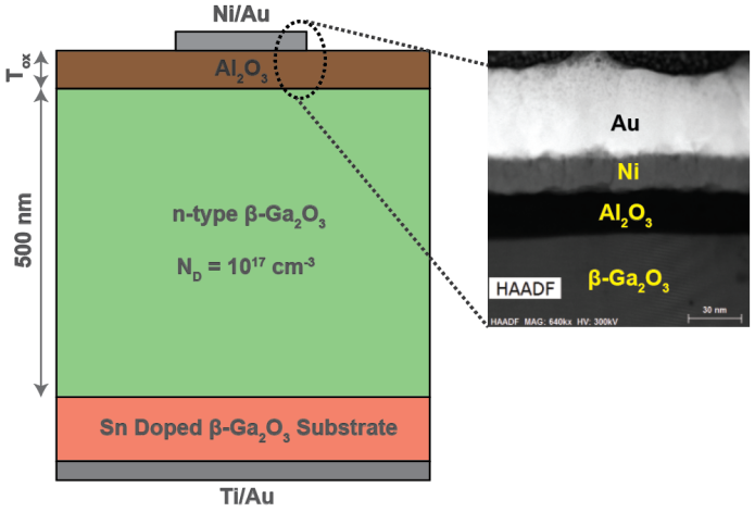
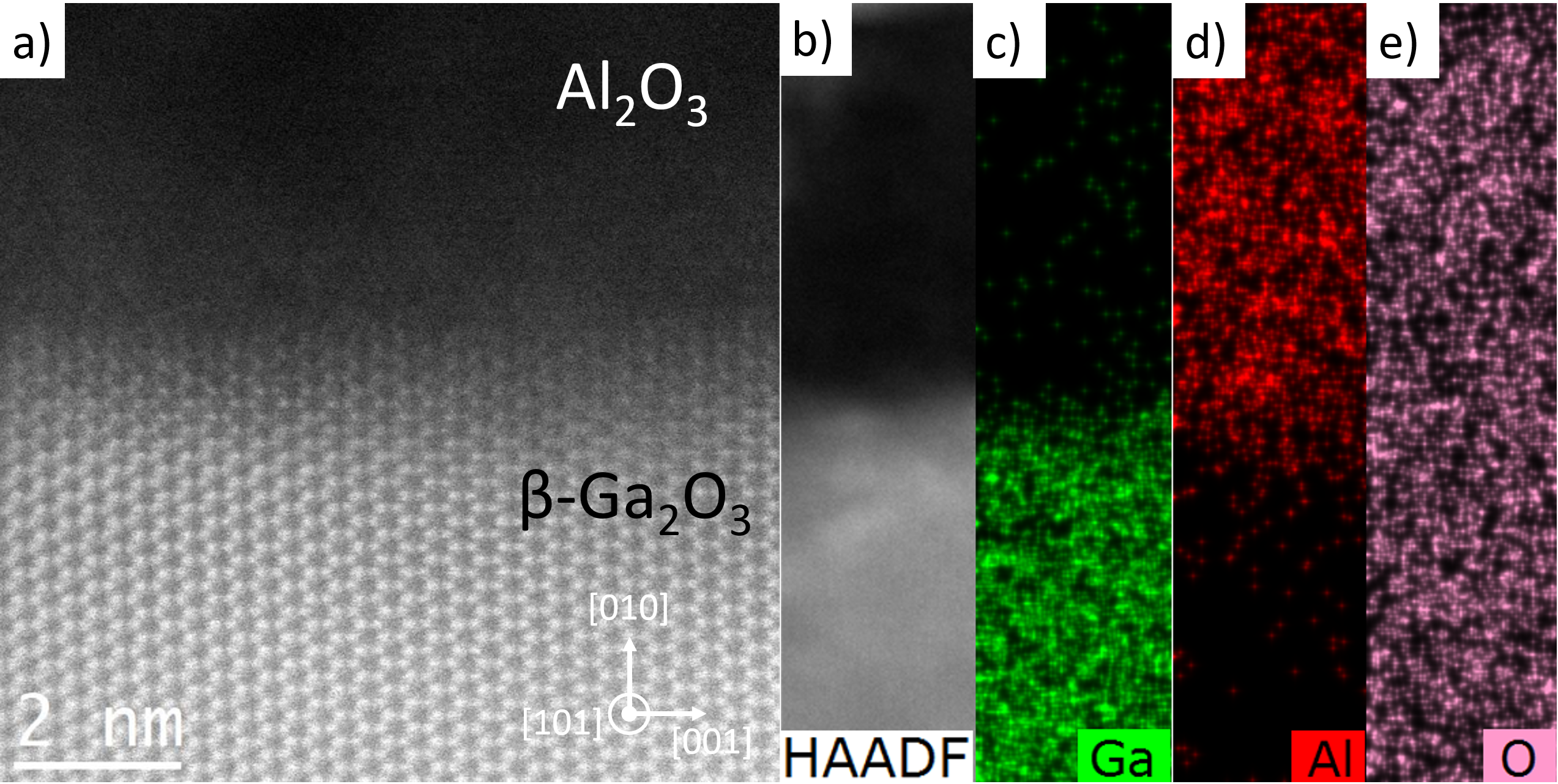
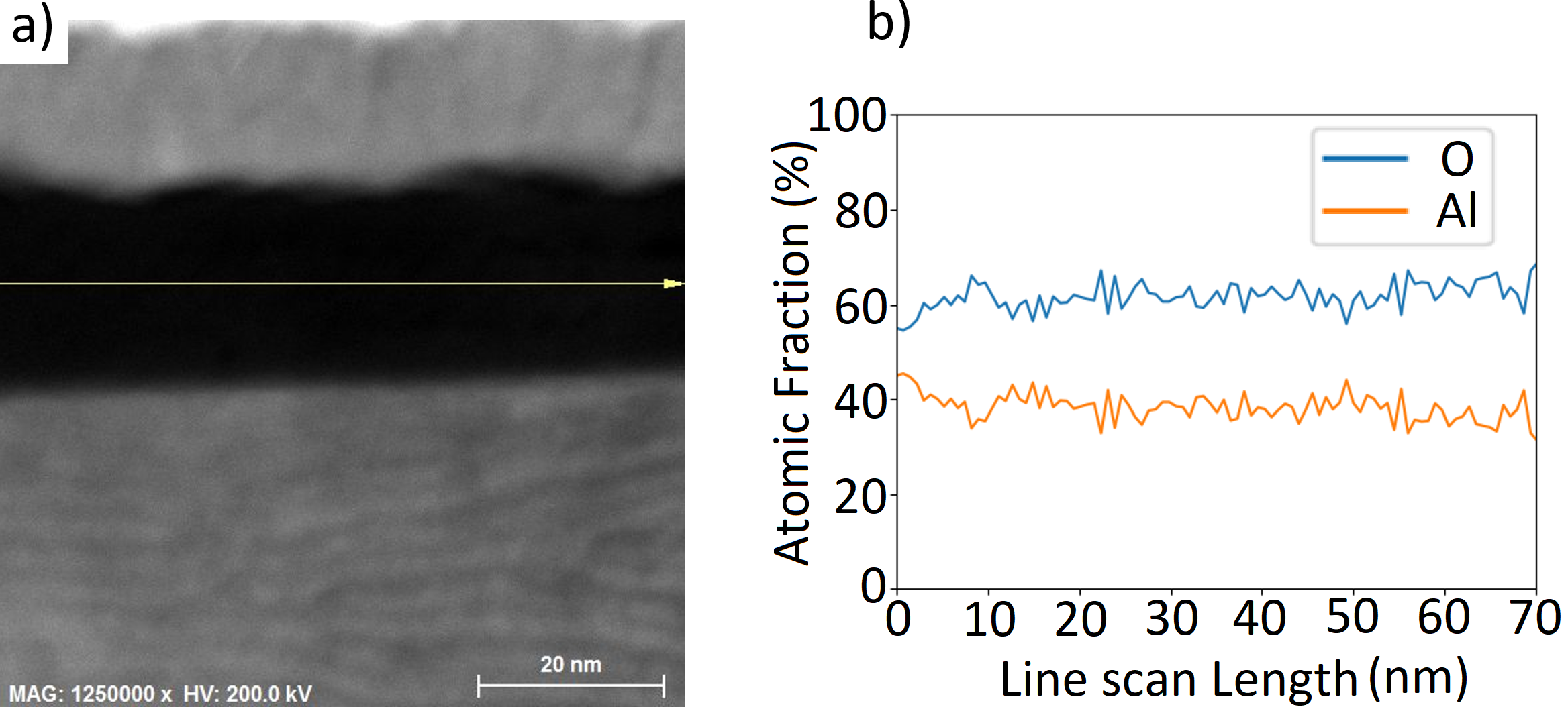
The growth of in-situ Al2O3 layer after the epitaxial growth of -Ga2O3 on Sn doped (010) -Ga2O3 and the fabrication of MOSCAPs as shown in Figure 1 to analyze the in-situ Al2O3/-Ga2O3 interface quality is discussed in the experimental section. To evaluate the abruptness of the Al2O3/-Ga2O3 interface as well as the stoichiometry of the Al2O3, scanning transmission electron microscope imaging within a high angle annular dark field detector (HAADF-STEM) combined with energy dispersive x-ray spectroscopy (EDS) were used on a cross-section of the interface prepared by focused ion beam (FEI Helios 660). HAADF-STEM images were performed using a FEI Titan G2 60-300 STEM with an acceleration voltage of 300kV, a condenser lens aperture of 70 µm and a probe current of about 100 pA. Figure 2 (a) shows a HAADF-STEM image of the Al2O3/-Ga2O3 interface in the [101] projection in which the -Ga2O3 substrate is brighter then the Al2O3 film due to the heavier Ga atoms. The Al2O3/-Ga2O3 interface is found to be abrupt with a transitional region of about 2 nm in which Ga atoms contrast vanishes and the high resolution is lost. The abruptness of the Al2O3/-Ga2O3 interface was also confirmed by EDS mapping (Bruker) performed in the same region. Figure 2 (b) shows a HAADF-STEM image of the interface with its corresponding EDS maps of (c) Ga, (d) Al and (e) O. A smooth transition between the two materials is observed with a small diffusion of Al atoms at the top of the -Ga2O3 epilayer. In addition, the composition of Al2O3 could be extracted from the EDS mapping analysis using the Cliff-Lorimer ratio technique detailed in the supporting information.[26] As a result, the film reveals an uniform composition with 382 % of Al and 622 % of O and stays relatively homogeneous along the Al2O3 film as shown by the EDS linescan of Figure 3 (b).
To characterize the trap densities, the fabricated MOSCAPs with different thicknesses were subjected to a series of CV measurements using Keithley 4200, shown in Figure 3. The alternating current (AC) bias and frequency used were 30 mV and 1 MHz respectively and the MOSCAPs were swept at a rate of 200 mV/sec. The dielectric constant was extracted to be 8.2-8.5 from the accumulation capacitance on all three samples. The methodology used to extract the trap densities is same as the technique developed by Liu et. al. [22] and presented briefly here. The MOSCAPs were first taken from depletion (D) to accumulation (A) and kept at accumulation for 10 minutes to fill all the empty electron traps. After 10 minutes, they were again swept back to depletion (1st sweep). Another CV curve is measured by sweeping the MOSCAP from depletion to accumulation and immediately back from accumulation to depletion (2nd sweep). The total charge (QI) within the MOSCAPs is calculated from the equation (1),
| (1) |
where, VFB is the flat band voltage, Tox is the oxide thickness, V is the ideal flat band voltage, is the electron charge, is the relative permittivity of the Al2O3 layer, and is the absolute permittivity. Assuming all the charges are located at or near the oxide/semiconductor interface, QI can be determined from the linear fit of the VFB vs oxide thickness plot. The change in VFB for D to A and A to D sweeps of the hysteresis plot can be attributed to the total amount of initially empty trapped charge within the MOSCAPs as described by the equation (2),
| (2) |
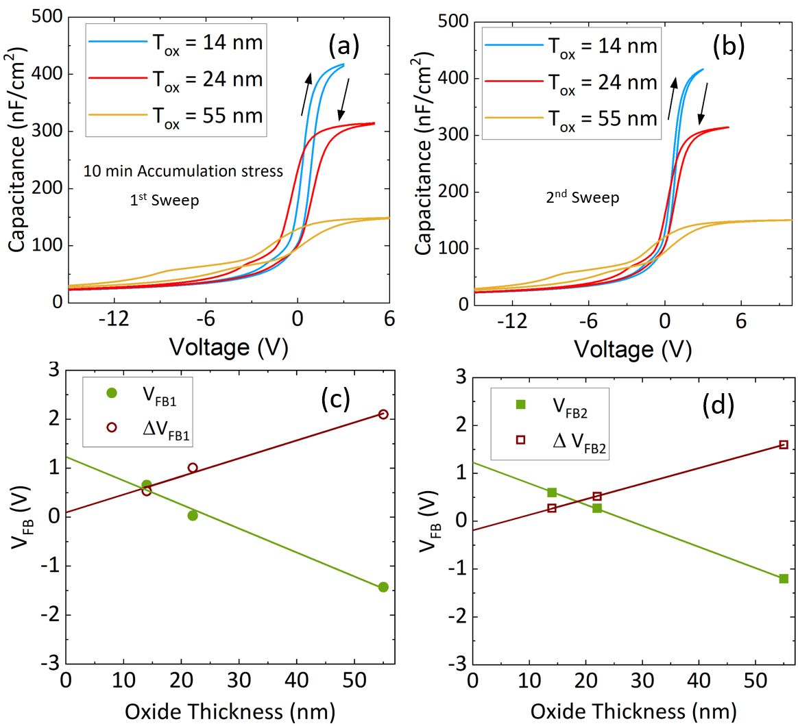
Where, VFB is the flat band voltage difference between the D to A and A to D sweeps and QT is the trapped electron density. Figure 4 (a) and (b) shows the 1st and 2nd sweeps of the CV hysteresis plots respectively for the MOSCAPs with three different Al2O3 thicknesses. The CV measurements were repeatable after the 2nd sweep, overlapping with the 2nd sweep measurements. Different forward bias voltages were applied for MOSCAPs with different Al2O3 thicknesses to maintain approximately same electric field through the oxide ( 2 MV/cm). Figure 4 (c) and (d) shows the corresponding VFB and VFB for the 1st and second sweeps. Flat band voltages were extracted from the deflection point of the capacitance voltage plot.[27] VFB1 and VFB2 are the flat band voltages calculated from the D to A sweeps of the 1st and 2nd sweep, respectively. Fixed charges (QI1 QI2) are determined from the slope of the flat band voltage vs oxide thickness plot. QI1 is the fixed charge of the MOSCAP without any bias history. So, QI2 is the total fixed near interface charge in the same MOSCAP, but also contains trapped electrons due to the measurement sweeps and 10 minutes of accumulation stress. Now, VFB1 and VFB2 are the flat band voltage differences, between each pair of D to A and A to D sweeps of the 1st and 2nd sweep respectively. During the 10 minutes of accumulation stress of the first hysteresis measurement electrons fill the empty slow near interface states and due to the high emission time of the slow traps these electrons remain trapped afterwards. However, electron will fill the fast near interface states also during the 10 min accumulation time. So, VFB1 can be attributed to the initially empty fast and slow near interface states (QT1). Only the fast traps will respond during the second hysteresis and subsequent measurements since the slow traps were filled during the first sweep. So VFB2 can be attributed to only the fast near interface states(QT2). Density of the initially empty slow near interface traps can be evaluated from the difference between QT1 and QT2 (). However, during the first D to A and A to D sweeps, there could be electron emission from some of the slow near interface states due to the applied reverse bias. So, the difference in flat band voltage for the D to A sweeps of 1st and 2nd sweep can be attributed to the more stably filled slow near interface states (QTS). All the fixed and trapped charges described here are summarized in Table 1. The positive fixed charge observed in this work is similar to the previous report of ALD Al2O3/ (-201) Ga2O3 interface.[7]
| QI1 | QI2 | QT1 | QT2 | QTS | |
| 2.3 1012 cm-2 | 2 1012 cm-2 | -1.7 1012 cm-2 | -1.2 1012 cm-2 | 5 1011 cm-2 | 3 1011 cm-2 |
The conduction band offset at the Al2O3/-Ga2O3 heterostructure can be evaluated using equation (3) as VFB can be written as,[7]
| (3) |
where, Eox is the electric field in the oxide at flat band condition due to the fixed charge at the, is Ni/Al2O3 conduction band barrier height, the difference between the conduction band and fermi level in -Ga2O3, and EC is the conduction band offset between -Ga2O3 and Al2O3. was considered to be 3 eV as evaluated by Zhang et. al. using internal photoemission spectroscopy.[28] From Figure 4 (c) and (d), () is extracted to be 1.23 eV. Using equation 3, the value of EC is calculated to be 1.7 eV which matches well with the previous reports on the ALD Al2O3/-Ga2O3 heterostructure.
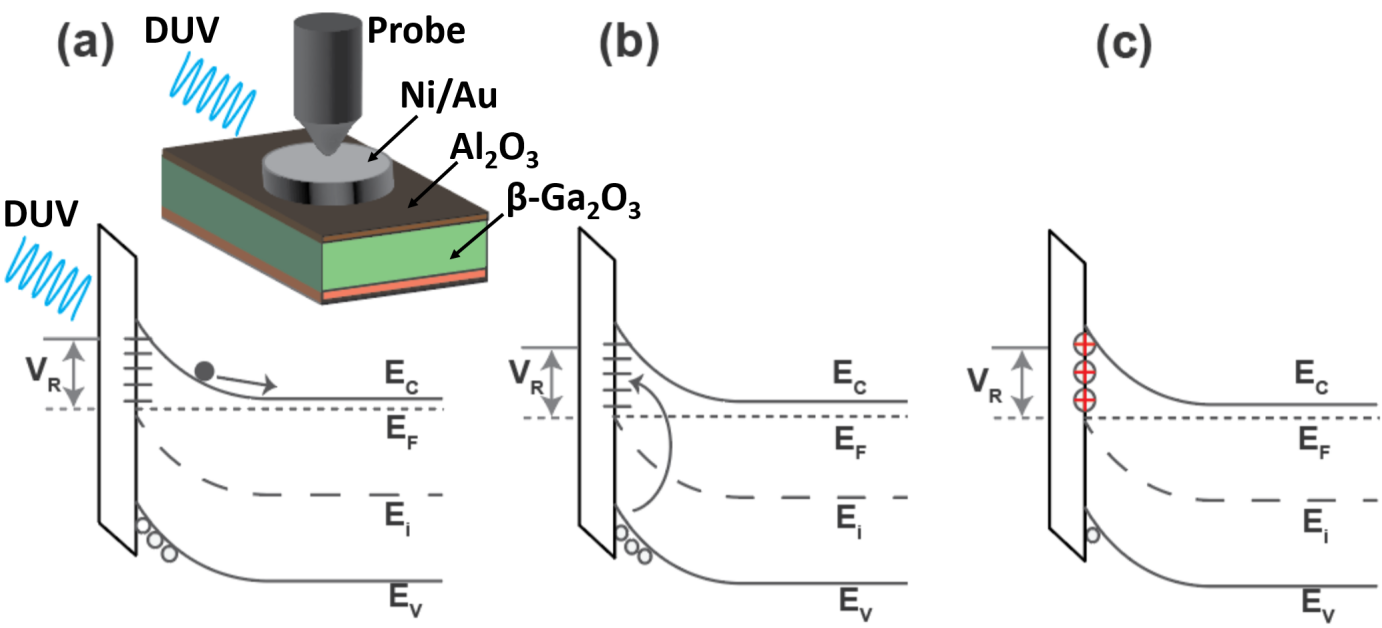
Now, to find the density of all the initially filled slow near interface states and the trap distribution as a function of energy dependence near the -Ga2O3 band edge, we use UV assisted CV technique developed by Swenson et. al.[29] and later modified by Liu et. al.[30] This technique was also used by Jian et. al.[20] for ALD Al2O3/(001) -Ga2O3 MOSCAPs and briefly summarized here. The MOSCAPs were first taken from D to A and kept at accumulation for 10 minutes to fill all the interface states. After 10 minutes time the MOSCAPs were again swept back to depletion without any optical excitation. This dark curve is considered as the ideal CV curve, assuming all the states are filled with electrons. Next the MOSCAPs were held at depletion and were exposed to UV light using a DUV LED with 254 nm wavelength for 5 minutes. After 5 minutes the UV light is turned off and the MOSCAPs were held at depletion for 15 minutes followed by another sweep from D to A. The dark curve is then shifted horizontally to match the post DUV CV curve and obtained as the reference CV curve. The total density of the all the interface states is calculated from the difference between the post DUV and the reference CV curve (V) and their energy dependence is calculated from the amount of band bending (dielectric/semiconductor surface potential) that occurs during the bias sweep.
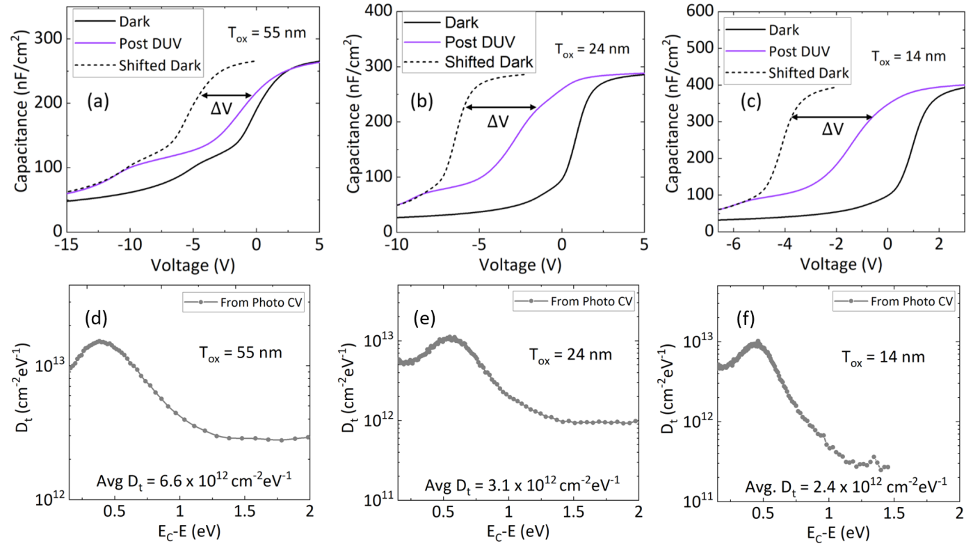
Figure 5 (a) to (c) shows energy band diagrams of the MOSCAPs under applied bias and UV illumination. During the UV exposure, electron hole pairs are generated and the photo-generated holes either recombine with the electrons trapped in the interface or gets self-trapped, which results in the ledge observed in the post DUV curve. Due to the recombination of photo generated holes with the trapped electrons at the Al2O3/-Ga2O3 interface, the trapped states become positively charged, which changes the width of the depletion region. Some of the extra holes also get trapped in the dielectric bulk hole traps inside the Al2O3 layer. Figure 6 (a) to (c) shows CV plots for the MOSCAPs with three different oxide thicknesses. The black curve (Dark) is the A to D sweep after the 10 minutes of accumulation stress. The purple curve is the D to A sweep after DUV exposure and the dashed black curve is the reference curve obtained after shifting the dark curve to match the post DUV plot. V in Figure 6 (a) to (c) includes the effects of both interface traps at the Al2O3/-Ga2O3 interface and bulk hole traps inside the Al2O3 layer. Density of all the initially filled interface and bulk dielectric traps is calculated using the equation (4),
| (4) |
where, is the surface potential at the Al2O3/-Ga2O3 interface, given by = . ND is the doping density, is the area of the contacts, Cdep is the depletion capacitance and Cox is the oxide capacitance.
Figure 6 (d) to (f) shows the Dt vs the trap energy distribution for the MOSCAPs with three different oxide thicknesses. Due to the existence of a positive valence band offset, the extra holes (which did not recombine with the interface traps) get accumulated at the Al2O3/-Ga2O3 interface (some holes also get self-trapped). The rise in the Dt near the conduction band edge can be attributed to the accumulated holes, either at the Al2O3/-Ga2O3 interface or possibly also due to the self-trapped holes in the depletion region.[31] The average Dt for each of the MOSCAPs are obtained after eliminating the contribution from holes by neglecting the rise in Dt.
We can also see from Figure 6 (d) to (f) that the average Dt reduces as the thickness of the Al2O3 layer decreases. There would not be any dielectric thickness dependence if all the traps were located at the Al2O3/-Ga2O3 interface. Instead, due to the presence of bulk hole traps inside the Al2O3 layer, some of the holes get captured inside the Al2O3 layer. So, the density of the interface states (Dit) without the contribution from the bulk hole traps in the Al2O3 is calculated from the equation (5).[30]
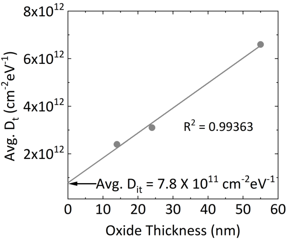
| (5) |
Where, nht is the amount of bulk hole traps inside the Al2O3. So, average Dit is obtained to be 7.8 1011 cm-2 eV-1 by extrapolating the linear fit of average Dt vs oxide thickness for Tox = 0 as shown in Figure 7. The amount of bulk hole traps (nht) is estimated from the equation 5 to be 2.1 1017 cm-3 eV-1. The fact that we see a linear relationship of Dt vs oxide thickness clearly indicates that not all the holes are self-trapped in the -Ga2O3 and in-fact can move and get inside the Al2O3 layer and get trapped. The mobility of holes could be significant enough to cause bulk hole trapping in the dielectric as also extracted by Akyol [32] for -Ga2O3 schottky barrier diode based photodetector. The value of Dit obtained for the in-situ Al2O3 MOSCAPs are significantly lower than the previous reports of ALD Al2O3/ (001) -Ga2O3 interface and may have resulted from the O vacancies and Al dangling bonds at the interface.
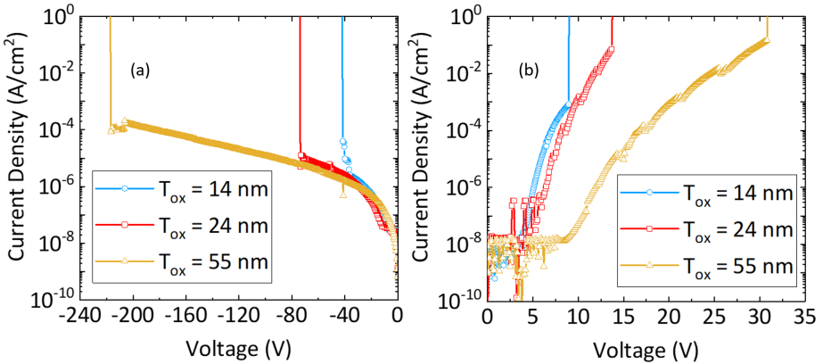
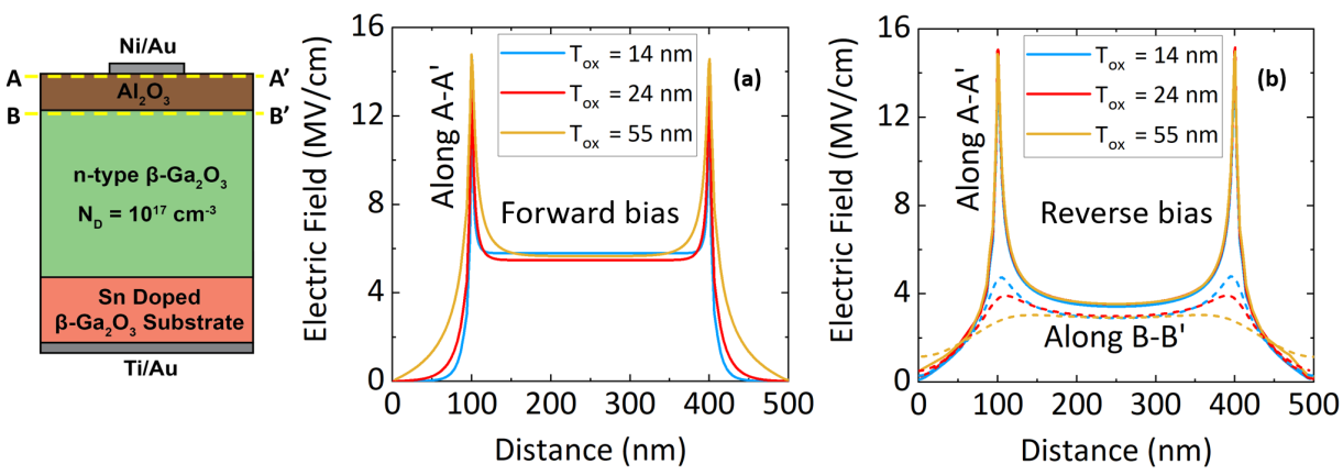
To determine leakage currents and breakdown voltages of the MOSCAPs, reverse and forward current voltage (IV) characteristics is measured and shown in Figure 8 (a) and (b) respectively. The measurement is performed at a sweep rate of 200 mV/sec. Breakdown voltages with positive bias on the gate metal (accumulation) for MOSCAPs with 14, 24 and 55 nm Al2O3 thicknesses are 9, 14, and 32 V, respectively. The breakdown field for all the MOSCAPs were determined using Sentaurus device simulator[33] and the field profile is shown in Figure 9 (a). For the accumulation case with positive potential on the gate, the entire voltage is dropped across the Al2O3 layer and so the breakdown can be attributed to the breakdown of the dielectric. The average breakdown field at the center of the gate metal region and peak field at the edges of the metal for the Al2O3 dielectric are estimated to be 5.8 MV/cm and 15 MV/cm respectively from electric field simulations as shown in Figure 9 (a). Electric fields were shown only in the Al2O3 region during forward bias as the entire bias voltage is dropped across the oxide layer. The barrier to tunneling for the MOSCAPs were also estimated using trap assisted tunneling model and extracted to be 1.1 eV and presented in the supporting information. The reverse breakdown voltage from the IV characteristics in Figure 8 (a) for MOSCAPs with 14, 24 and 55 nm Al2O3 thicknesses are approximately 40, 80, and 200 V, respectively. From the electric field distribution in Figure 9 (b), a peak field of 15 MV/cm is observed at the metal edges but the center of the gate metal, the electric field is less than the observed field in case of forward bias ( 3.5 MV/cm as compared to 5.8 MV/cm). This is due to the fact that, at reverse bias, the total applied voltage is dropped across both Al2O3 and Ga2O3 region and a significant amount of electric field is present in the Ga2O3 ( 2.6 MV/cm) as also shown by the dashed curves in Figure 9 (b). At reverse bias, all the three MOSCAPs (Tox = 14, 24 and 55 nm) have a peak electric field of around 15 MV/cm, indicating that the breakdown is probably happening at the metal edges. These high edge electric fields can be reduced by creating a field plate structure using the same in-situ Al2O3 material showing the versatility of this technique.
The in-situ Al2O3 grown using MOCVD, in this work, is found to have reduced fixed charges and interface traps (Dit) compared to the more commonly used ALD technique. A lower fixed charge concentration of +2 × 1012 cm-2 is found when compared to ALD Al2O3 on (-201) -Ga2O3 (+3.6 1012 cm-2) reported by Hung et. al.[7] A lower interface trap density (Dit) of 7.8 1011 cm-2eV-1 is also found in comparison to ALD Al2O3/ (001) -Ga2O3 interface reported by Jian et. al. (1.34 1012 cm-2eV-1).[20] It is to be noted that no high temperature post deposition annealing (PDA) or post metallization annealing (PMA) is performed on these MOSCAPs, which is expected to further improve the interface quality.[34] Further experiments to understand the effect of growth parameters such as growth temperature, chamber pressure and precursor ratios and also higher temperature PDA will be necessary to improve the dielectric constant, fixed charge, interface traps and critical breakdown fields of the Al2O3 layers in these fully MOCVD-grown Al2O3/-Ga2O3 MOSCAPs. Also, detailed work is necessary to investigate the origin of the interface traps which may have resulted from native defects and impurities at the interface and can be performed using structural and spectroscopic techniques.
In conclusion, we report in-situ Al2O3 growth using MOCVD as a potentially better alternative to ALD and the interface quality is investigated using capacitance voltage characterization. The presence of near interface fixed charge in these MOSCAPs were identified and quantified using the linear relationship between flat band voltage and oxide thicknesses and a stable positive fixed charge of +2 1012 cm-2 is calculated. The sheet density of trap states with fast and slow emission times were also calculated from linear relationship of the CV hysteresis versus Al2O3 thickness plots. The density of all the near interface traps and their energy dependence were calculated using UV-assisted CV technique as low as +7.8 1011 cm-2. Conduction band offset using the linear relationship between flat band voltage and oxide thicknesses is calculated to be 1.7 eV. Furthermore, the average breakdown fields for the MOCVD grown Al2O3 material is found to be approximately 5.8 MV/cm. This approach of in-situ dielectric deposition on -Ga2O3 can pave the way as gate dielectrics for future -Ga2O3 based high performance MOSFETs due to its promise of improved interface and bulk quality compared to other conventional dielectric deposition techniques.
Experimental Section
The MOSCAP fabrication started with the growth of a 500 nm -Ga2O3 epilayer on Sn-doped bulk (010) -Ga2O3 substrates (NCT Japan) using Agnitron MOVPE reactor with far injection showerhead design. Prior to loading the sample in the growth chamber, the substrates were cleaned using acetone, methanol and DI water and followed by a 15 min dip in HF solution. Triethylgallium (TEGa) and O2 were used as the precursors, Ar as the carrier gas and diluted silane as the dopant. The growth process of -Ga2O3 was performed at a low temperature of 600 0C and at a chamber pressure of 60 Torr.[35, 36] The gas flow values for TEGa and O2 were set to 65 and 800 sccm and the Ar flow rate was set to 1100 sccm. A silane flow rate of 0.06 nmol/min was used to achieve a silicon doping concentration of 1017 cm-3. After the Ga2O3 growth, a 30 second purge step was used to purge all the unreacted precursors from the reactor. During this purge step, the reactor pressure was ramped down from 60 to 15 Torr whereas the temperature is kept same at 600 0C. The O2 flow rate was also reduced from 800 to 500 sccm during this 30 second purge step. Following this, growth time of the Al2O3 layer was varied to achieve dielectric thicknesses of 14, 24 and 55 nm, on three different substrates. In-situ Al2O3 was grown at a growth rate of 1.2 nm/min using the Trimethylaluminum (TMAl) precursor with a flow rate of 5.33 mol/min and O2 with a flow rate of 500 sccm. To find the thickness of the dielectric Al2O3 layer, the samples were patterned using photolithography and the Al2O3 dielectric layer was etched away using buffered oxide etch (BOE) with photoresist as the mask. The etch depth is measured using atomic force microscopy and the details are provided in the supporting information. After the growth of the Al2O3 layer, Ti (50 nm)/Au (100nm) ohmic contacts were sputter deposited on the back side of the MOSCAPs. Finally, circular Ni (10 nm)/Au (50 nm) gate contacts were patterned using standard photolithography and deposited on the Al2O3 surface using E-beam evaporation.
Supporting Information
Supporting Information is available from the author.
Acknowledgements
This material is based upon work supported by the Air Force Office of Scientific Research under Award Number FA9550-18-1-0507 (Program Manager: Dr. Ali Sayir). Any opinions, findings, and conclusions or recommendations expressed in this material are those of the author(s) and do not necessarily reflect the views of the United States Air Force. The authors also acknowledge funding from the National Science Foundation (NSF) through Grant DMR-1931652. The work at Penn State University was supported by the Air Force Office of Scientific Research (AFOSR) program FA9550-18-1-0277 and GAME MURI, 10059059-PENN.
References
- [1] S. Pearton, J. Yang, P. H. Cary IV, F. Ren, J. Kim, M. J. Tadjer, M. A. Mastro, Applied Physics Reviews 2018, 5, 1 011301.
- [2] S. Stepanov, V. Nikolaev, V. Bougrov, A. Romanov, Rev. Adv. Mater. Sci 2016, 44 63.
- [3] K. Zeng, Y. Jia, U. Singisetti, IEEE Electron Device Letters 2016, 37, 7 906.
- [4] K. Zeng, U. Singisetti, Applied Physics Letters 2017, 111, 12 122108.
- [5] K. D. Chabak, J. P. McCandless, N. A. Moser, A. J. Green, K. Mahalingam, A. Crespo, N. Hendricks, B. M. Howe, S. E. Tetlak, K. Leedy, R. C. Fitch, D. Wakimoto, K. Sasaki, A. Kuramata, G. H. Jessen, IEEE Electron Device Letters 2018, 39, 1 67.
- [6] A. J. Green, K. D. Chabak, M. Baldini, N. Moser, R. Gilbert, R. C. Fitch, G. Wagner, Z. Galazka, J. Mccandless, A. Crespo, K. Leedy, G. H. Jessen, IEEE Electron Device Letters 2017, 38, 6 790.
- [7] T.-H. Hung, K. Sasaki, A. Kuramata, D. N. Nath, P. Sung Park, C. Polchinski, S. Rajan, Applied Physics Letters 2014, 104, 16 162106.
- [8] D. Biswas, C. Joishi, J. Biswas, K. Thakar, S. Rajan, S. Lodha, Applied Physics Letters 2019, 114, 21 212106.
- [9] P. H. Carey IV, J. Yang, F. Ren, R. Sharma, M. Law, S. J. Pearton, ECS Journal of Solid State Science and Technology 2019, 8, 7 Q3221.
- [10] N. A. Moser, J. P. McCandless, A. Crespo, K. D. Leedy, A. J. Green, E. R. Heller, K. D. Chabak, N. Peixoto, G. H. Jessen, Applied Physics Letters 2017, 110, 14 143505.
- [11] N. K. Kalarickal, Z. Feng, A. F. M. Anhar Uddin Bhuiyan, Z. Xia, W. Moore, J. F. McGlone, A. R. Arehart, S. A. Ringel, H. Zhao, S. Rajan, IEEE Transactions on Electron Devices 2021, 68, 1 29.
- [12] Z. Xia, H. Chandrasekar, W. Moore, C. Wang, A. J. Lee, J. McGlone, N. K. Kalarickal, A. Arehart, S. Ringel, F. Yang, et al., Applied Physics Letters 2019, 115, 25 252104.
- [13] H. N. Masten, J. D. Phillips, R. L. Peterson, IEEE Transactions on Electron Devices 2019, 66, 6 2489.
- [14] K. D. Chabak, D. E. Walker, A. J. Green, A. Crespo, M. Lindquist, K. Leedy, S. Tetlak, R. Gilbert, N. A. Moser, G. Jessen, In 2018 IEEE MTT-S International Microwave Workshop Series on Advanced Materials and Processes for RF and THz Applications (IMWS-AMP). 2018 1–3.
- [15] K. D. Chabak, N. Moser, A. J. Green, D. E. Walker Jr, S. E. Tetlak, E. Heller, A. Crespo, R. Fitch, J. P. McCandless, K. Leedy, et al., Applied Physics Letters 2016, 109, 21 213501.
- [16] A. J. Green, K. D. Chabak, E. R. Heller, R. C. Fitch, M. Baldini, A. Fiedler, K. Irmscher, G. Wagner, Z. Galazka, S. E. Tetlak, A. Crespo, K. Leedy, G. H. Jessen, IEEE Electron Device Letters 2016, 37, 7 902.
- [17] W. Li, K. Nomoto, Z. Hu, T. Nakamura, D. Jena, H. G. Xing, In 2019 IEEE International Electron Devices Meeting (IEDM). 2019 12.4.1–12.4.4.
- [18] W. Li, K. Nomoto, Z. Hu, D. Jena, H. G. Xing, IEEE Electron Device Letters 2020, 41, 1 107.
- [19] W. Li, K. Nomoto, Z. Hu, D. Jena, H. G. Xing, In 2019 Device Research Conference (DRC). 2019 209–210.
- [20] Z. Jian, S. Mohanty, E. Ahmadi, Applied Physics Letters 2020, 116, 24 242105.
- [21] X. Liu, S. Chan, F. Wu, Y. Li, S. Keller, J. Speck, U. Mishra, Journal of crystal growth 2014, 408 78.
- [22] X. Liu, J. Kim, R. Yeluri, S. Lal, H. Li, J. Lu, S. Keller, B. Mazumder, J. Speck, U. Mishra, Journal of Applied Physics 2013, 114, 16 164507.
- [23] X. Liu, R. Yeluri, J. Kim, S. Lal, A. Raman, C. Lund, S. Wienecke, J. Lu, M. Laurent, S. Keller, et al., Applied Physics Letters 2013, 103, 5 053509.
- [24] X. Liu, J. Kim, D. Suntrup, S. Wienecke, M. Tahhan, R. Yeluri, S. Chan, J. Lu, H. Li, S. Keller, et al., Applied Physics Letters 2014, 104, 26 263511.
- [25] C. Gupta, S. H. Chan, A. Agarwal, N. Hatui, S. Keller, U. K. Mishra, IEEE Electron Device Letters 2017, 38, 11 1575.
- [26] G. Cliff, G. Lorimer, Journal of Microscopy 1975, 103, 2 203.
- [27] R. Winter, J. Ahn, P. C. McIntyre, M. Eizenberg, Journal of Vacuum Science & Technology B, Nanotechnology and Microelectronics: Materials, Processing, Measurement, and Phenomena 2013, 31, 3 030604.
- [28] Z. Zhang, C. M. Jackson, A. R. Arehart, B. McSkimming, J. S. Speck, S. A. Ringel, Journal of electronic materials 2014, 43, 4 828.
- [29] B. Swenson, U. Mishra, Journal of Applied Physics 2009, 106, 6 064902.
- [30] W. Liu, I. Sayed, C. Gupta, H. Li, S. Keller, U. Mishra, Applied Physics Letters 2020, 116, 2 022104.
- [31] R. Yeluri, X. Liu, B. L. Swenson, J. Lu, S. Keller, U. K. Mishra, Journal of Applied Physics 2013, 114, 8 083718.
- [32] F. Akyol, Journal of Applied Physics 2020, 127, 7 074501.
- [33] Sentaurus Device User Manual, (Version N-2017.09, March 2017).
- [34] S. H. Chan, Ph.D. thesis, UC Santa Barbara, 2018.
- [35] A. Bhattacharyya, P. Ranga, S. Roy, J. Ogle, L. Whittaker-Brooks, S. Krishnamoorthy, Applied Physics Letters 2020, 117, 14 142102.
- [36] P. Ranga, A. Bhattacharyya, A. Chmielewski, S. Roy, N. Alem, S. Krishnamoorthy, Applied Physics Letters 2020, 117, 17 172105.