Imaging and Spectral Performance of a 60 m Pitch CdTe Double-Sided Strip Detector
Abstract
We have evaluated the performance of a fine pitch CdTe Double-sided Strip Detector (CdTe-DSD), which was originally developed for the focal plane detector of a hard X-ray telescope to observe the Sun. The detector has a thickness of 750 m and has 128 strip electrodes with a 60 m strip pitch orthogonally placed on both sides of the detector and covers an energy range 4 keV to 80 keV. The study of the depth of photon interaction and charge sharing effects are of importance in order to provide good spectroscopic and imaging performance. We study the tail structure observed in the spectra caused by charge trapping and develop a new method to reconstruct the spectra based on induced charge information from both anode and cathode strips. By applying this method, energy resolutions (FWHM) of 0.76 keV and 1.0 keV can be obtained at photon energies of 14 keV and 60 keV, respectively, if the energy difference between the anode and cathode is within 1 keV. Furthermore, the tail component at 60 keV is reduced, and the energy resolution of the 60 keV peak is improved from 2.4 keV to 1.5 keV (FWHM) if the energy difference is greater than 1 keV. In order to study the imaging performance, we constructed a simple imaging system using a 5 mm thick tungsten plate that has a pinhole with a diameter of 100 m. We utilize a 133Ba radioisotope of 1 mm in diameter as a target source in combination with a 100 m slit made from 0.5 mm thickness tungsten. We imaged the 133Ba source behind the 100 m slit using a 30 keV peak, with a 100 m pinhole placed at the center of the source-detector distance. By applying a charge sharing correction between strips, we have succeeded in obtaining a position resolution better than the strip pitch of 60 m.
keywords:
X-ray, CdTe, double-sided strip detector1 Introduction
Semiconductor detectors for spectroscopy and imaging of hard X-ray photons at several tens of keV are now playing an important role in various research fields, from X-ray astronomy to non-destructive material analysis and in vivo medical imaging. Recently high resolution, photon counting, imaging spectrometers have emerged as attractive technologies for these applications, in which images and spectra are obtained simultaneously from the interaction position and the energy of each photon.
To achieve high energy resolution and high position resolution at the same time, we have been developing CdTe Double-sided Strip Detectors (CdTe-DSD), based on a CdTe diode[takahashi1999high, takahashi2001recent], ranging from a strip pitch of 250 m to 60 m [Watanabecdte2009, takahashi2017high], in combination with dedicated readout electronics [takahashi2001high, Nakazawa2004, Takahashi2005]. Imaging is achieved by orthogonal strip electrodes on the two sides of the detectors[Katsuragawa2018, Takeda2018, Ishikawa2016].
One merit of the DSD configuration is that signals can be processed with a smaller number of electronic channels than in the case of a pixel configuration, which generally means more space for complex circuits for low noise amplification. Furthermore, signals generated by the movement of carriers in the device can be measured from both the anode strips and the cathode strips. products in CdTe are known to be small in comparison with other semiconductor devices, such as Si and Ge, and there is a factor of about ten in this product between electrons and holes. Therefore the total amount of induced charge for a given photon energy depends on the distance between the interaction point and the electrode due to the hole trapping in the device and it is expected that these signals carry information regarding the depth of interaction.
Another piece of information we can obtain from the configuration of fine pitch strips is the charge spread. It has been reported that the charge clouds generated in sensors are spread across multiple pixels, if pixel sizes are reduced to the extent of the clouds[Koenig2013].
This suggests that the spread of the cloud over multiple strips on the DSD could be used to reconstruct the interaction location in the detector which improves the position resolution to a level finer than the strip pitch.
Following onto our previous publication[Furukawa2018], we have performed a detailed study of the characteristics of a fine pitch CdTe-DSD using 60 m pitch strips, which was originally developed for the focal plane detector for a hard X-ray telescope used in the third flight of a sounding rocket experiment, named the Focusing Optics X-ray Solar Imager (FOXSI-3) which was used to observe the Sun[Glesener2016, Musset2019]. In this paper, we report significant improvements in the spectral performance by comparing the pulse height measured from anode and cathode strips to correct the effects of depth of interaction, caused by hole trapping. We also report the improvement of image resolution by properly taking the charge spread into account.
2 Detector Configurations
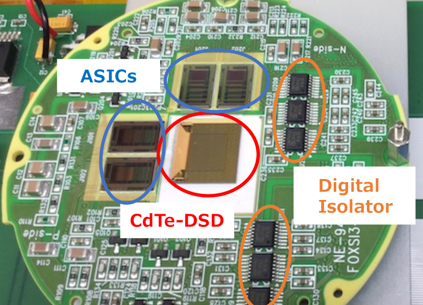
Our experiment uses a detector made for the FOXSI-3 experiment. Figure 1 shows a picture of a Front End Card (FEC) of the 60 m pitch CdTe-DSD for FOXSI and a system diagram of an experimental setup for calibration data acquisition. The detector has a thickness of 750 m and covers an energy range of 4 keV to 80 keV. It has 128 strip electrodes on each side and the width of each strip electrode is 50 m with a 10 m gap between the strips. The imaging area is 7.68 7.68 mm2. More details are described in [Furukawa2018].
The CdTe sensor is connected to four Application Specific Integrated Circuits (ASICs) for pulse height measurement. Each ASIC has 64 channels and each channel contains a preamplifier, fast shaper for self-triggering and slow shaper for pulse height measurement[Watanabe2014]. Anode and cathode electrodes are placed orthogonal to each other and pulse heights from both sides reflect 2-dimensional information on where X-rays intersect the device.

3 Spectroscopic Performance
3.1 Anode and Cathode spectrum of 241Am
The CdTe-DSD provides two independent measurements of energy from its anode and cathode electrodes. Figure 2 shows two 241Am spectra obtained by the two sides of the detector. The detector was irradiated on the cathode side. If energy is detected on two or more adjacent strips (multi-strip event), the total sum of energies on the adjacent strips are used. In the anode side spectrum, energy resolutions are 1.1 keV at 14 keV and 1.4 keV at 60 keV in FWHM. Below 20 keV, the cathode side spectrum is almost identical to that of the anode side. In contrast, the peaks above 20 keV exhibit low-energy tails. This tail structure is caused by the depth dependence of the induced charge due to the charge trapping effect[takahashi2001recent, salcin2014, He2001].
When high energy photons (20 keV) enter the detector, some of the photons penetrate relatively deeply into the detector and the depth of interaction (DoI) is a vertically spread distribution. As the DoI becomes deeper, the total measured energy on the cathode electrodes gets smaller, creating a tail on the peak toward low energies. Figure 3 compares the energies measured by the cathode and anode sides. The low-energy tail on the 60 keV cathode-side peak is indicated by the red region. For low energies (20 keV), the anode and cathode energy spectra are almost identical and averaging both measurements results in the expected energy resolution improvement[Watanabecdte2009]. However, for higher energies (20 keV), a more complicated correction is required to improve the energy resolution. We have applied an algorithm applicable up to at least 60 keV, confirming the spectroscopic performance improvement across the entire range.


3.2 Averaged Spectra
When the anode side energy and the cathode side energy are equal within a certain margin, a simple average works well to obtain a superior energy resolution. Figure 4 shows the averaged spectrum when the difference between the anode and cathode side energy is within the energy resolution. The energy resolution at 14 keV is 1.1 keV(FWHM) or 0.47 keV() in both the anode and cathode spectra. The 1 resolution of the energy difference () is 0.66 keV. In this paper we define of the combined energy as the margin in which simple averaging is utilized.
Below 23 keV, most of the events fall in this margin shown by the blue region in Figure. 3. If the energy resolution is dominated an effect of the readout electronics on each side, the energy resolution will improve by by averaging the energies measured by the anode side and cathode side. The improved energy resolution of 0.76 keV in the averaged spectrum is highly consistent with this number.
However, when the difference is larger than the threshold, the same method is no longer useful and only results in a degradation of energy resolution. This is due to the tail structure shown in the red region in Figure. 3. At high energies, most events do not fall in the margin and it would degrade the lack of detection efficiency at high energy if we only use the events in the margin. To achieve the best possible energy resolution while mitigating the loss of events, this tail structure must be corrected.

3.3 Tail angle and its distribution
To correct the tail structure, we define a tail angle as the angle between the horizontal axis and the tail structure axis. To calculate the angle, principle component analysis (PCA) is used and the tail structure axis is defined as the first principal component axis, i.e. the direction that maximizes the data variance along the axis (Figure 5(a)). For the actual analysis, we utilized the TPrincipal class in ROOT framework[brun1997]. To apply this framework, counts are distributed randomly in each bin of a 2-dimensional histogram of the energy average and difference of both sides and bins with less than three counts are ignored. We calculate the tail angle for every pixel, using principal component analysis, and make a distribution of the tail angle for all pixels (Figure 5(b)). The standard deviation is 1.2 degrees, which is approximately 2% of the peak value. From this result we assume theta is constant across pixels and independent of measured energy for a given branch on the plot, and is well represented by its peak value. By using the peak value of the tail angle , we can reconstruct the correct energy.


3.4 Reconstruction algorithm and improved spectra
The incident energy reconstruction algorithm used in this paper is as follows:
If the absolute energy difference between the anode and cathode energies is
-
1.
within 1.0 keV: keV
The reconstructed energy is equal to the average energy. -
2.
less than keV: keV
The reconstruction function is the linear combination of the difference and the average of the energies, with the reconstructed energy contour line aligned parallel to the tail-like structure. Tail angles are calculated by PCA in each pixel of the detector. The peak of the distribution for all pixels is used as the representative value . -
3.
greater than 1.0 keV: keV
The tail angle is determined as 55.3∘ by the PCA on the energy ”average vs difference” plot summed over the detector. It is assumed that the tail structure in this case is caused by the events which photons interact very close to the cathode side[salcin2014] and the percentage of this event is 5.3%.
By applying this method, the energy resolution of 60 keV peak is improved. In Figure 6, 60 keV peaks in the averaged spectrum (blue) and the spectrum obtained by the above method (red) with an energy difference greater than 1 keV are compared. The averaged spectrum with an energy difference within 1 keV (black) is also superimposed. While averaging fails to correct the tail structure, the method introduced in this section allows to mitigate the degradation of energy resolution even when the energy difference is large. By using this tail-corrected spectrum, the lack of efficiency at high energy is mitigated while keeping the energy resolution.

4 Properties of charge splitting
4.1 The Dependence on the incident photon energy
The energy of incident photons can be properly reconstructed by using the method discussed in the previous section. This makes it possible to accurately assess the energy dependence of charge shared events. Figure 7 shows the incident photon energy and the degree of charge sharing between adjacent strips. As the incident photon energy increases, the charge shared event increases for both sides. It is thought that since the initial charge cloud size is roughly proportional to the incident energy (due to electrostatic repulsion) the fraction of multiple events increases for higher energies. There is also the effect that multiple events are more likely to detect at high energies because the energy threshold of each strip is set at 1.5 keV

4.2 The Dependence on the depth of photon interaction
We examine the relationship between the depth of photon interaction and the ratio of charge shared events. It is to be noted that the difference between the cathode and anode side energy represents the depth of photon interaction. If photons interact near the surface of the anode side, more holes are trapped and a lower energy than expected is observed in the cathode side. Figure 8 represents the correlation of the energy difference (i.e. photon interaction depth) and ratio of charge shared events. As photons interact near the surface of the anode side, charge shared events at the cathode side increase. This indicates that the longer the charge takes to travel to the electrodes, the more likely it is that a charge shared event occurs.
