Hybrid Integration of GaP Photonic Crystal Cavities with Silicon-Vacancy Centers in Diamond by Stamp-Transfer
Abstract
Optically addressable solid-state defects are emerging as one of the most promising qubit platforms for quantum networks. Maximizing photon-defect interaction by nanophotonic cavity coupling is key to network efficiency. We demonstrate fabrication of gallium phosphide 1-D photonic crystal waveguide cavities on a silicon oxide carrier and subsequent integration with implanted silicon-vacancy (SiV) centers in diamond using a stamp-transfer technique. The stamping process avoids diamond etching and allows fine-tuning of the cavities prior to integration. After transfer to diamond, we measure cavity quality factors () of up to 8900 and perform resonant excitation of single SiV centers coupled to these cavities. For a cavity with of 4100, we observe a three-fold lifetime reduction on-resonance, corresponding to a maximum potential cooperativity of . These results indicate promise for high photon-defect interaction in a platform which avoids fabrication of the quantum defect host crystal.
In an optical quantum network, quantum entanglement is distributed among spatially separated stationary qubit nodes through flying qubits (photons) [1], enabling long-range quantum communication [2] and distributed quantum computing [3]. Optically addressable defects [4] in materials like diamond [5, 6], silicon carbide [7, 8], ZnO [9] and rare-earth doped crystals [10, 11] show tremendous potential for realization of such stationary qubit nodes. Efficient generation and utilization of flying qubits can be enabled by on-chip photonic integration of defect qubits. Here, we demonstrate a hybrid-photonic architecture in diamond, integrating single negatively charged silicon-vacancy qubits with waveguide integrated gallium phosphide (GaP) photonic crystal (PhC) cavities [12].
Negatively charged silicon-vacancy (SiV) centers in high-quality diamond crystals show nearly lifetime-limited optical transitions for centers created by ion-implantation and vacuum annealing [13]. The favorable spectral behavior of the SiV center can be attributed to its inversion symmetry which protects the optical transitions from electric field noise in the environment [14, 15]. This protection has enabled efficient coupling of SiV centers to monolithic diamond photonic structures [16]. Here we explore an alternative planar geometry that eliminates diamond etching, potentially minimizing fabrication-induced damage to the defect environment. Photonic cavities are fabricated on an intermediate GaP on silicon-oxide carrier chip and then transferred to a diamond sample with implanted SiV defects via a polymer stamping process [17, 12]. The hybrid stamp transfer process will allow independent optimization of the SiV qubits and the photonic structures. Commercial wafer scale implementations of stamp-transfer pick-and-place hybrid photonic integration processes [18, 19, 20] suggest good prospects for scalable assembly of defect-cavity interfaces with ancillary devices such as detectors, switches, filters and passive photonic components.
In our experiments, we demonstrate single SiV qubits coupled to GaP photonic cavities. We observe a quality factors on the silicon oxide carrier exceeding and upto after stamp transfer to the diamond substrate. For a cavity with a we see a three-fold reduction in the coupled SiV lifetime with the cavity on-resonance. The observed lifetime reduction corresponds to a minimum cavity Purcell enhancement of 30 and maximum possible cooperativity of 2 for the coupled SiV center.
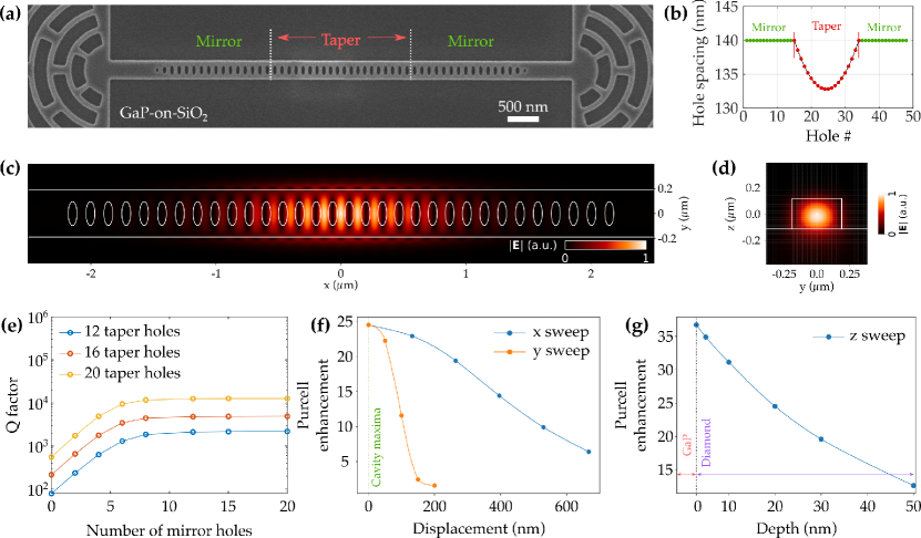
The device consists of a 1-D array of elliptical holes etched into the GaP (Fig. 1a). The designed GaP layer thickness is constrained to 222 nm. A unit cell of the cavity consists of a single elliptical hole with major-axis and minor-axis , GaP width and a lattice constant . The of the cavity can be divided into the taper and mirror sections as shown in Fig. 1b. Within the mirror region, the hole periodicity, , is chosen to maximize the TE quasi-band gap around the target frequency of the SiV zero-phonon transition at 737 nm. Within the taper region, the hole periodicity is adiabatically reduced from so as to create a defect mode for the target frequency. The presence of the high index diamond substrate underneath the GaP introduces design challenges towards achieving high because the substrate expands the light-line such that photons can couple to the continuum of modes in the diamond and thus leak out of the cavity. Full details of the cavity design and optimization can be found in Ref.[21, 12].
We restrict the minimum feature size to be 70 nm due to fabrication limitations. The optimized design, with nm is simulated using finite-difference time-domain method (FDTD, Lumerical). A driven dipole source modeling the SiV is placed within the evanescent cavity field. The time-decay of the cavity mode and measured radiated power is utilized to estimate the resonator characteristics and tolerance to dipole placement (Fig. 1c-g, see SI.7 for details). For a defect 20 nm beneath the GaP-diamond interface a Purcell enhancement as high as 25 is possible, which increases to 35 at 3 nm beneath the interface.
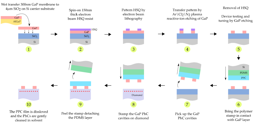
The cavity structure is fabricated using a 300 nm GaP membrane (Fig. 2:1-5) that is released from a GaP substrate by etching an intermediate sacrificial layer with dilute HF. The GaP membrane is then transferred to a silicon-oxide on Si substrate using a wet-transfer process [22, 23, 24]. Electron-beam lithography is performed using hydrogen silsesquioxane (HSQ) resist to pattern the cavity devices. Subsequent inductively coupled plasma reactive-ion-etching (RIE) of the GaP layer forms the photonic devices.
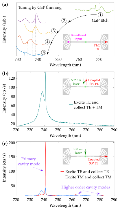
The GaP-on-oxide cavity devices are characterized before stamp transfer to diamond. The resonances of individual devices are identified by using a supercontinuum laser (600 to 800 nm, see SI.1) to obtain the transmission spectra. The excitation is linearly polarized, and matched to the TE resonator mode. Scattered excitation light was filtered from the collection path via spatial filtering. We measure cavity resonances near 770 nm (Fig. 3a-1) strongly red-shifted from design. The red-shift is due to the initial GaP height of 300 nm which is thicker than the design specification of 222 nm.
To couple the GaP cavity devices to SiV qubits, the distribution of cavity resonances needs to be centered around the SiV ZPL wavelength of 737 nm. Here we target 731 nm as stamp transfer from the SiO2 carrier chip to higher index diamond is expected to red-shift the resonances by nm. We blue-shift the cavity resonances by iterative thinning of the GaP layer (Fig. 3a: spectra 1–5) using a short blanket GaP RIE plasma etch (15 s for step-1, 8 s for steps-2 to 5; GaP etch rate 100 nm/min). After each etch cycle, the GaP-on-oxide cavity transmission is measured to track the resonance blue-shift. After thinning, many cavities exhibit quality factors at the spectrometer limit (Q). We measure a final GaP thickness of 225 nm (SI.2).
A chemical vapor deposition diamond (Element Six, electronic grade, N 5 ppb, B 1 ppb) is implanted with Si accelerated to 26 keV (5e11 cm-2 dose, 7∘ angle) and vacuum annealed at 1200 ∘C for 2 hrs. During annealing, SiV centers are formed by vacancy diffusion and recombination with the implanted silicon, yielding a layer of SiV centers 20 nm from the surface ( 50 SiV centers per 800 nm diameter excitation spot).
To transfer the cavities to the diamond, a stamping procedure [21, 25] is utilized, as shown in (Fig. 2:6-10). The process is carried out in a flip-chip wafer-bonder which controls both pressure and temperature. The process uses a PDMS stamp fabricated into a mesa structure and an intermediate polypropylene carbonate (PPC) film. The PDMS/PPC stack is brought in contact with the devices and heated to 60∘ C to promote adhesion. Next, the PDMS/PPC/cavity stack is lifted-off the carrier substrate. The diamond substrate is cleaned in a piranha 3:1 bath prior to stamping. The PDMS/PPC/cavity stack is aligned and pressed down on the diamond substrate. The stamp and diamond are heated to 130∘ C, which softens the PPC layer to release the PPC film from the PDMS stamp. Finally, we dissolve the PPC in trichloroethylene and soak the diamond in acetone followed by IPA.
Following the GaP transfer to diamond, cavity transmission measurements are performed. We observe resonances for all 28 intact transferred cavities, with resonance wavelengths in the range of 730 to 755 nm. Remarkably, many stamped devices show cavity resonances with quality factors between 5,000 to 8,900, close to the design goal of 10,000 (SI.3.).
Room-temperature photoluminescence (PL) measurements are performed to study SiV coupling to the stamped GaP photonic devices. We excite with an off-resonant 532 nm laser and collect SiV PL normal to the sample at the excitation position (Fig. 3b). At room-temperature, the SiV PL spectra consists of a zero-phonon line (ZPL) at 738 nm (full-width-half-max (FWHM) of 5 nm) and a broad phonon-sideband (PSB) (744 to 800 nm). We observe increased SiV ZPL emission at the cavity resonance along with a significant background ZPL contribution from other SiV centers within the excitation spot. By collecting the SiV PL coupled into the waveguide at the output grating, we observe a significantly larger fraction of SiV ZPL intensity at the cavity resonance with minimal background SiV contribution (Fig. 3c). Further, we observe a clear polarization dependence for the coupled SiV PL consistent with the designed TE cavity mode. These results confirm that an optical interface has been established between the diamond and the stamped GaP PhC cavity.
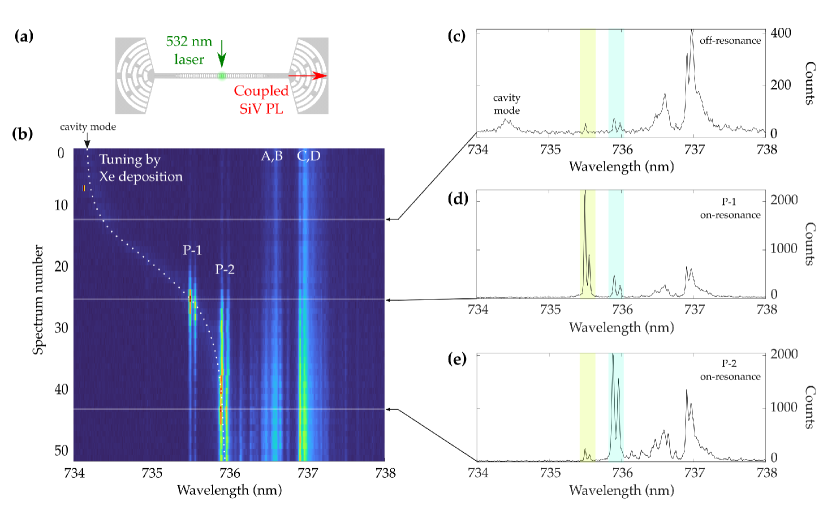
When cooled to 10 K, the cavity mode of the devices are blue-detuned from room-temperature by 5.5 nm due to the temperature dependence of the GaP index. Utilizing the 532 nm off-resonant excitation at the cavity center (Fig. 4a), we can monitor the cavity mode and SiV ZPL transitions at the output grating. Typical spectra shows four bright lines near 737 nm corresponding to the characteristic A–D transitions for SiV [14], together with a number of faint detuned lines associated with strained single SiV centers. The cavity mode can be red-shifted by injecting xenon gas into the sample chamber. The xenon condenses on the sample, increasing the effective index of the cavity mode and resulting in a controlled resonance shift as demonstrated in Fig. 4b. The maximum range of the xenon-induced red-shift is 1.9 nm. Although all 28 intact devices from the stamped array exhibit cavity resonances, only the nine devices having resonances within 3 nm of nm are utilized for xenon tuning measurements (Fig. 4c). For all nine devices, we are able to observe significant increase in PL on resonance for a range of SiV transitions from blue to red detuned with respect to the ensemble A–D lines (Fig. 4b; other devices in SI.4).
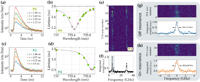
To facilitate coupling to single SiV transitions and for ease of cavity-mode identification, we focus on a device with isolated blue-detuned SiV transitions. We select device-3 with 4,100 which exhibits the maximum increase in PL of all devices. For this device, the cavity mode is tuned through two pairs of SiV ZPL denoted P-1 and P-2 (Fig. 4c-e). In order to quantify the SiV-cavity coupling we first perform time-resolved PL measurements while tuning the cavity over P-1 and P-2. We excite at the cavity with pulsed excitation at 704 nm (500 µW average power, 2 ps pulse width and 80 MHz repetition rate) and collect PL through the output grating, thus filtering only the cavity-coupled SiV. We then spectrally filter the PL via a spectrometer (0.2 nm bandwidth, centered on P-1 or P-2) and detect the PL with an avalanche photodiode. A low-intensity continuous-wave (20 µW) 532 nm laser is added to help stabilize the negative SiV charge state (SI.6). By fitting the temporally resolved PL (Fig. 5a,c, see SI.8 for details), we observe a reduction of the lifetime on resonance by a factor of
A plot of the lifetime as a function of cavity detuning (Fig. 5b,d) exhibits a Lorentzian lineshape, with a linewidth that is broader than the cavity resonance (FWHM0.17 nm). This is consistent with the broadening expected due to the contributions from the two SiV transitions comprising each pair (with separation of about nm and nm for P-1 and P-2 respectively).
Next, we perform photoluminescience excitation (PLE) spectroscopy to characterize the optical linewidths off and on cavity resonance. The SiV is resonantly excited via a low-power tunable diode laser which is scanned over the ZPL transition under consideration while the phonon sideband PL is collected ( nm) from above the cavity (as this emission is not resonant with the cavity). We observe distinct and consistent lines corresponding to ZPL P-1 (Fig. 5e-h) and P-2 (SI.5) by exciting either through the input grating or directly on the cavity. To maintain constant excitation intensity at the SiV during the scan, we select the latter configuration. Between different SiV centers, the excitation power was varied from 100 nW to 1 µW to optimize the signal-to-noise while minimizing SiV ionization. Additionally, a low-intensity blue LED and/or 532 nm pulse enabled consistent repumping of the SiV (SI.5).
We focus on ZPL P-1 due to the larger tuning range of the cavity. Fig. 5e shows a series of PLE scans over ZPL P-1 with the cavity red detuned by approximately 0.7 nm. Two bright lines are observed to be separated by about 25 GHz, consistent with the separation measured in PL. The off-resonant lifetime of ZPL P-1 measured in Fig. 5a was determined to be ns which corresponds to a lifetime-limited linewidth MHz. The additional broadening of the lines is understood to be a result of a combination of homogeneous phonon-broadening (limit of 250 MHz at 10 K [26]) and spectral diffusion. Because the broadening due to pure lifetime reduction is expected to be MHz, we focus on the highlighted line near GHz as it is significantly narrower than the other line near 30 GHz. While performing PLE scans centered on this line, we tune the cavity from the original red-detuned position into resonance (Fig. 5g,h). We measure a modest broadening of the overall linewidth by MHz which is consistent with the estimated broadening via the lifetime measurements.
The lifetime and linewidth measurements can be utilized to determine the Purcell enhancement and cooperativity of the SiV-cavity system. The SiV-cavity system can be modeled as an open system where the cavity is a purely additive decay channel with cavity loss rates and defect loss rates (including both radiative and non-radiative channels outside of the cavity). A Jaynes-Cummings Hamiltonian with single-photon Rabi frequency describes the SiV-cavity interaction (SI.7). If we consider only contributions to which describe population decay (i.e. ignore pure dephasing) and assume that the system is in the “bad-cavity” regime (), we may define the Purcell enhancement F as the multiplicative increase in the decay rate of the desired transition [27],
| (1) |
Here is the unit-normalized mode electric-field profile, is the SiV-cavity (angular) frequency detuning, and is a unit vector in the direction of the transition’s dipole moment. The constant is the well-known Purcell factor for a cavity with mode volume at wavelength [28].
Further assuming that the emitter’s proximity to the cavity does not substantially modify , we can determine the ratio of the off-resonant () and on-resonant () lifetimes to be given by
| (2) |
Comparing Eq. 2 to Eq. 1 enables estimation of the resonant Purcell enhancement via the relation
| (3) |
where is intrinsic spontaneous emission rate of the relevant transition. The factor is an intrinsic (cavity-independent) property of the emitter and may be estimated from the quantum efficiency , Debye-Waller factor , and ZPL branching ratio as (SI.7). Taking conservative estimates of [29], [30], and [31] provides an upper-bound of , and thus a lower bound on the Purcell enhancement of P-1 and P-2. Using the measured lifetime data (Fig.5) we find
which are within the range of feasible Purcell enhancement (Fig. 1(f,g)).
Additionally, the cooperativity of the SiV-cavity system can be defined as where is the pure-dephasing rate. Using the total off-resonant linewidth MHz and lifetime-limited linewidth MHz, we are able to estimate the cooperativity of the P-1 transition under consideration as
| (4) |
Reducing the temperature to eliminate the thermal photon broadening beyond the lifetime limit is expected to reduce the total linewidth to MHz. Provided the other broadening mechanisms are temperature independent, this would result in a cooperativity of . If the SiV linewidth was lifetime limited (i.e. no pure dephasing), then the maximum expected cooperativity for P-1 is given to be . Similarly for P-2, assuming the pure depahsing is of similar magnitude ( MHz), we estimate a cooperativity of , increasing to below the thermal-broadening limit, and with a maximum value for a lifetime-limited linewidth of .
Although the SiV studied here do not have lifetime-limited linewidths, similar ranges of broadening were observed in other implanted SiV that were not coupled to devices (SI.5). This suggests that a sample with improved defect linewidths could potentially achieve cooperativities with little modification to the fabrication process. Additionally, since current devices are operating near the design limit, higher can be achieved with further design optimization. Relaxing the design limit on the minimum PhC hole dimension from nm to nm leads to an increase of by a factor of . Additionally, stamping of the cavity along the crystal axis or utilizing a diamond with surface orientation could result in improvements to the coupling coefficient by up to a factor of 4. This indicates that can be achieved in hybrid device geometries despite the low refractive index contrast. This regime is promising for applications such as optical spin readout [32], quantum-optical switches and tunable single-photon sources [16], and quantum repeaters [33].
In summary, we have demonstrated significant coupling between a GaP cavity and diamond SiV qubit avoiding all fabrication of the diamond substrate. Before integration the cavities can be characterized and tuned close to the specific target resonance wavelength. This enables optimization of the SiV-cavity coupling yield with the potential for minimal disruption to the qubit environment within the diamond. For the transferred GaP-on-diamond cavities, we measure quality factors close to the design target. Current device properties should enable cooperativity , with a promising outlook for with modest design improvements. These results highlight the promise of hybrid photonic architectures for quantum network applications, even in relatively low-index contrast material combinations.
I Supporting information
Schematic of microscope system, Images of fabricated devices, Room-temperature transmission spectra of GaP-on-diamond devices, Tuning curves on different devices, Resonant excitation measurements on both device and non-device SiV, Intensity dependence of SiV photoluminescence with 532 nm and 700 nm excitation, Theory and simulation of the SiV-cavity system, Fits and error approximation.
II Acknowledgements
This material is based upon work supported by Department of Energy, Office of Science, National Quantum Information Science Research Centers, Co-design Center for Quantum Advantage (C2QA) under contract number DE-SC0012704 and National Science Foundation Grant No. ECCS-1807566. N.S.Y. was supported by the National Science Foundation Graduate Research Fellowship Program under Grant No. DGE-2140004. A.A. was supported by a Post Graduate Scholarship from the Natural Sciences and Engineering Research Council of Canada (PGSD3 - 545932 - 2020). D.H. was supported by the National Science Scholarship from A*STAR, Singapore. The photonic devices were fabricated at the Washington Nanofabrication Facility, a National Nanotechnology Coordinated Infrastructure (NNCI) site at the University of Washington which is supported in part by funds from the National Science Foundation (awards NNCI-2025489, 1542101, 1337840 and 0335765). The authors acknowledge the use of Princeton’s Imaging and Analysis Center, which is partially supported through the Princeton Center for Complex Materials (PCCM), a National Science Foundation (NSF)-MRSEC program (DMR-2011750) as well as the Princeton Micro-Nano Fabrication Lab.
References
- [1] M. Ruf, N. H. Wan, H. Choi, D. Englund, and R. Hanson, “Quantum networks based on color centers in diamond,” Journal of Applied Physics, vol. 130, no. 7, p. 070901, 2021.
- [2] S. Wehner, D. Elkouss, and R. Hanson, “Quantum internet: A vision for the road ahead,” Science, vol. 362, no. 6412, 2018.
- [3] D. Kielpinski, C. Monroe, and D. J. Wineland, “Architecture for a large-scale ion-trap quantum computer,” Nature, vol. 417, p. 709, 2002.
- [4] L. C. Bassett, A. Alkauskas, A. L. Exarhos, and K.-M. C. Fu, “Quantum defects by design,” Nanophotonics, vol. 8, no. 11, pp. 1867–1888, 2019.
- [5] M. W. Doherty, N. B. Manson, P. Delaney, F. Jelezko, J. Wrachtrup, and L. C. Hollenberg, “The nitrogen-vacancy colour centre in diamond,” Physics Reports, vol. 528, pp. 1–45, July 2013.
- [6] C. Bradac, W. Gao, J. Forneris, M. E. Trusheim, and I. Aharonovich, “Quantum nanophotonics with group IV defects in diamond,” Nature Communications, vol. 10, p. 5625, Dec. 2019.
- [7] M. Radulaski, M. Widmann, M. Niethammer, J. L. Zhang, S.-Y. Lee, T. Rendler, K. G. Lagoudakis, N. T. Son, E. Janzén, T. Ohshima, J. Wrachtrup, and J. Vučković, “Scalable Quantum Photonics with Single Color Centers in Silicon Carbide,” Nano Letters, vol. 17, pp. 1782–1786, Mar. 2017.
- [8] K. C. Miao, J. P. Blanton, C. P. Anderson, A. Bourassa, A. L. Crook, G. Wolfowicz, H. Abe, T. Ohshima, and D. D. Awschalom, “Universal coherence protection in a solid-state spin qubit,” arXiv preprint arXiv:2005.06082, 2020.
- [9] M. L. Viitaniemi, C. Zimmermann, V. Niaouris, S. H. D’Ambrosia, X. Wang, E. S. Kumar, F. Mohammadbeigi, S. P. Watkins, and K.-M. C. Fu, “Coherent spin preparation of indium donor qubits in single zno nanowires,” Nano Letters, vol. 22, no. 5, pp. 2134–2139, 2022.
- [10] T. Zhong, J. M. Kindem, J. G. Bartholomew, J. Rochman, I. Craiciu, E. Miyazono, M. Bettinelli, E. Cavalli, V. Verma, S. W. Nam, F. Marsili, M. D. Shaw, A. D. Beyer, and A. Faraon, “Nanophotonic rare-earth quantum memory with optically controlled retrieval,” Science, vol. 357, pp. 1392–1395, Sept. 2017.
- [11] M. Raha, S. Chen, C. M. Phenicie, S. Ourari, A. M. Dibos, and J. D. Thompson, “Optical quantum nondemolition measurement of a single rare earth ion qubit,” Nature communications, vol. 11, no. 1, pp. 1–6, 2020.
- [12] D. Huang, A. Abulnaga, S. Welinski, M. Raha, J. D. Thompson, and N. P. de Leon, “Hybrid iii-v diamond photonic platform for quantum nodes based on neutral silicon vacancy centers in diamond,” Opt. Express, vol. 29, pp. 9174–9189, Mar 2021.
- [13] J. Lang, S. Häußler, J. Fuhrmann, R. Waltrich, S. Laddha, J. Scharpf, A. Kubanek, B. Naydenov, and F. Jelezko, “Long optical coherence times of shallow-implanted, negatively charged silicon vacancy centers in diamond,” Applied Physics Letters, vol. 116, no. 6, p. 064001, 2020.
- [14] C. Hepp, T. Müller, V. Waselowski, J. N. Becker, B. Pingault, H. Sternschulte, D. Steinmüller-Nethl, A. Gali, J. R. Maze, M. Atatüre, et al., “Electronic structure of the silicon vacancy color center in diamond,” Physical Review Letters, vol. 112, no. 3, p. 036405, 2014.
- [15] A. Sipahigil, K. Jahnke, L. Rogers, T. Teraji, J. Isoya, A. Zibrov, F. Jelezko, and M. Lukin, “Indistinguishable Photons from Separated Silicon-Vacancy Centers in Diamond,” Physical Review Letters, vol. 113, p. 113602, Sept. 2014.
- [16] A. Sipahigil, R. E. Evans, D. D. Sukachev, M. J. Burek, J. Borregaard, M. K. Bhaskar, C. T. Nguyen, J. L. Pacheco, H. A. Atikian, C. Meuwly, et al., “An integrated diamond nanophotonics platform for quantum-optical networks,” Science, vol. 354, no. 6314, pp. 847–850, 2016.
- [17] A. Dibos, M. Raha, C. Phenicie, and J. Thompson, “Atomic Source of Single Photons in the Telecom Band,” Physical Review Letters, vol. 120, p. 243601, June 2018.
- [18] C. O. de Beeck, B. Haq, L. Elsinger, A. Gocalinska, E. Pelucchi, B. Corbett, G. Roelkens, and B. Kuyken, “Heterogeneous iii-v on silicon nitride amplifiers and lasers via microtransfer printing,” Optica, vol. 7, no. 5, pp. 386–393, 2020.
- [19] M. Heck, “Inspire: Inp on sin photonic integrated circuits realized through wafer-scale micro-transfer printing,” in Integrated Photonics Platforms II, vol. 12148, pp. 88–92, SPIE, 2022.
- [20] M. Billet, L. Reis, Y. Léger, C. Cornet, F. Raineri, I. Sagnes, K. Pantzas, G. Beaudoin, G. Roelkens, F. Leo, et al., “Gallium phosphide-on-insulator integrated photonic structures fabricated using micro-transfer printing,” Optical Materials Express, vol. 12, no. 9, pp. 3731–3737, 2022.
- [21] M. Raha, A Telecom-Compatible Quantum Memory in the Solid-State: Single Erbium Ions Coupled to Silicon Nanophotonic Circuits. PhD thesis, Princeton University, 2021.
- [22] E. Yablonovitch, D. M. Hwang, T. J. Gmitter, L. T. Florez, and J. P. Harbison, “Van der Waals bonding of GaAs epitaxial liftoff films onto arbitrary substrates,” Applied Physics Letters, vol. 56, pp. 2419–2421, June 1990.
- [23] E. R. Schmidgall, S. Chakravarthi, M. Gould, I. R. Christen, K. Hestroffer, F. Hatami, and K.-M. C. Fu, “Frequency Control of Single Quantum Emitters in Integrated Photonic Circuits,” Nano Letters, vol. 18, pp. 1175–1179, Feb. 2018.
- [24] S. Chakravarthi, P. Chao, C. Pederson, S. Molesky, A. Ivanov, K. Hestroffer, F. Hatami, A. W. Rodriguez, and K.-M. C. Fu, “Inverse-designed photon extractors for optically addressable defect qubits,” Optica, vol. 7, p. 1805, Dec. 2020.
- [25] D. Huang, Building Quantum Network Nodes Based on Neutral Silicon Vacancy Centers in Diamond. PhD thesis, Princeton University, 2021.
- [26] K. D. Jahnke, A. Sipahigil, J. M. Binder, M. W. Doherty, M. Metsch, L. J. Rogers, N. B. Manson, M. D. Lukin, and F. Jelezko, “Electron–phonon processes of the silicon-vacancy centre in diamond,” New Journal of Physics, vol. 17, no. 4, p. 043011, 2015.
- [27] A. Faraon, P. E. Barclay, C. Santori, K.-M. C. Fu, and R. G. Beausoleil, “Resonant enhancement of the zero-phonon emission from a colour centre in a diamond cavity,” Nature Photonics, vol. 5, no. 5, pp. 301–305, 2011.
- [28] E. M. Purcell, “Proceedings of the american physical society,” Phys. Rev., vol. 69, pp. 674–674, Jun 1946.
- [29] J. N. Becker and C. Becher, “Coherence properties and quantum control of silicon vacancy color centers in diamond,” physica status solidi (a), vol. 214, no. 11, p. 1700586, 2017.
- [30] E. Neu1, D. Steinmetz, J. Riedrich-Möller, S. Gsell, M. Fischer, M. Schreck, and C. Becher, “Single photon emission from silicon-vacancy colour centres in chemical vapour deposition nano-diamonds on iridium,” New J. Phys., vol. 13, p. 025012, Feb 2011.
- [31] J. L. Zhang, S. Sun, M. J. Burek, C. Dory, Y.-K. Tzeng, K. A. Fischer, Y. Kelaita, K. G. Lagoudakis, M. Radulaski, Z.-X. Shen, N. A. Melosh, S. Chu, M. Lončar, and J. Vučković, “Strongly cavity-enhanced spontaneous emission from silicon-vacancy centers in diamond,” Nano Letters, vol. 18, pp. 1360–1365, 02 2018.
- [32] L. J. Rogers, K. D. Jahnke, M. H. Metsch, A. Sipahigil, J. M. Binder, T. Teraji, H. Sumiya, J. Isoya, M. D. Lukin, P. Hemmer, et al., “All-optical initialization, readout, and coherent preparation of single silicon-vacancy spins in diamond,” Physical review letters, vol. 113, no. 26, p. 263602, 2014.
- [33] W. Dür, H.-J. Briegel, J. I. Cirac, and P. Zoller, “Quantum repeaters based on entanglement purification,” Phys. Rev. A, vol. 59, pp. 169–181, Jan 1999.