Gate-defined quantum point contacts in a germanium quantum well
Abstract
We report an experimental study of quantum point contacts defined in a high-quality strained germanium quantum well with layered electric gates. At zero magnetic field, we observe quantized conductance plateaus in units of 2. Bias-spectroscopy measurements reveal that the energy spacing between successive one-dimensional subbands ranges from 1.5 to 5 meV as a consequence of the small effective mass of the holes and the narrow gate constrictions. At finite magnetic fields perpendicular to the device plane, the edges of the conductance plateaus get splitted due to the Zeeman effect and Landé factors are estimated to be for the holes in the germanium quantum well. We demonstrate that all quantum point contacts in the same device have comparable performances, indicating a reliable and reproducible device fabrication process. Thus, our work lays a foundation for investigating multiple forefronts of physics in germanium-based quantum devices that require quantum point contacts as a building block.
Germanium (Ge) nanostructures are emerging as a pioneering research platform for pursuing multiple quantum computation schemes.Scappucci et al. (2021) This relies on the special properties in the holes of Ge, including strong spin-orbit interactionBulaev and Loss (2007); Moriya et al. (2014) and compatibility with superconducting components.Li et al. (2018); Tosato et al. (2023) Benefit from these properties, fast qubit operations in spin qubit processorsWatzinger et al. (2018); Hendrickx et al. (2020a, b, 2021); Froning et al. (2021); Jirovec et al. (2021, 2022); Wang et al. (2022) and high-quality semiconductor-superconductor hybridsRidderbos et al. (2020); Tosato et al. (2023) have been experimentally achieved in Ge nanostructures. Among the nanostructures, strained Ge quantum wells with two-dimensional hole gases are particularly attractive due to their flexibility in device preparationHendrickx et al. (2021) and capability in large-scale integration.Borsoi et al. (2023) On top of this, strained Ge quantum wells can be grown with hole mobility exceeding one million,Lodari et al. (2022); Kong et al. (2023) signifying its exceptionally low disorder and long coherence length. The high quality of this material would lead to weak charge noise influence in quantum devices and therefore guarantees a high performance of the hole spin qubits.Hendrickx et al. (2020b, 2021) Aside from spin qubits, high-mobility Ge quantum wells are also considered as a competing platform for non-Abelian Majorana zero modesAdelsberger et al. (2023); Luethi et al. (2023); Laubscher, Sau, and Sarma (2024) and pioneering work has been done on hybridizing Ge quantum wells with superconductors.Hendrickx et al. (2018, 2019); Vigneau et al. (2019); Aggarwal et al. (2021); Tosato et al. (2023); Valentini et al. (2024)
Quantum point contacts (QPCs), as a basic nanostructure, have been widely used in quantum devices, including tunnelling barriers,Fornieri et al. (2019) quantum dots,van der Wiel et al. (2002); Hanson et al. (2007) charge sensorsElzerman et al. (2004) and fractional quantum Hall state interferometers.Bartolomei et al. (2020); Nakamura et al. (2020, 2023) In general, QPCs feature quantized conductance as a consequence of ballistic charge transport through one-dimensional (1D) channels.van Wees et al. (1988); Wharam et al. (1988) Previously, QPCs have been mainly studied in III-V materials, such as GaAs heterostructures,van Wees et al. (1988); Wharam et al. (1988) InAs quantum wellsDebray et al. (2009); Mittag et al. (2019); Lee et al. (2019); Hsueh et al. (2022) and InSb quantum wells.Qu et al. (2016); Lei et al. (2021) In contrast, QPCs in strained Ge quantum wells are rarely studied.Gul et al. (2017); Mizokuchi et al. (2018); Gul et al. (2018) In the mean time, QPCs are a key component in aforementioned Ge-based quantum devices including spin qubit processors and semiconductor-superconductor hybrid devices. Therefore, QPCs in strained Ge quantum wells deserve to be investigated thoroughly, especially from their reproducibility perspective.
In this work, we have fabricated QPCs in a strained Ge quantum well and studied their physical properties by electrical transport measurements. The QPCs in the Ge quantum well are defined by layered electric gates. At zero magnetic field, the QPCs exhibit conductance quantization in units of , indicating a ballistic charge transport through the gate-defined 1D channels. Bias-spectroscopy measurements are then conducted and quantization energies between the 1D subbands are obtained with values from 1.5 to 5. The considerable quantization energies result from the small effective mass of the holes in Ge and the narrow gate constrictions in the device. With magnetic fields, the edges of the conductance plateaus get splitted due to the Zeeman effect and the Zeeman energies are quantified in bias-spectroscopy measurements. Then, Landé factors of the 1D subbands are estimated to be . Notably, all three QPCs fabricated in the same device show comparable behaviors as a confirmation of uniform device preparations. Thus, our work demonstrates a reliable way of constructing quantum devices in Ge quantum wells.
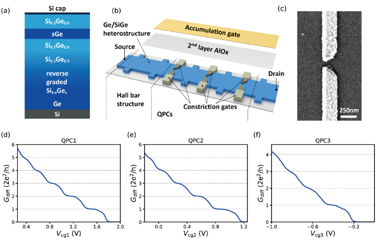
Figure 1(a) shows the layer structure of the Ge quantum well used in this work which is grown by reduced pressure chemical vapor deposition (RPCVD).Kong et al. (2023) The Ge/SiGe heterostructure is cultivated on a Si(001) substrate where Ge is initially grown. On top of this, there is a 1.31 m SiGe layer with gradually varied Si and Ge concentrations. A 10-nm thick Ge quantum well is subsequently grown, followed by a growth of Si0.2Ge0.8 as a top barrier layer. The heterostructure growth is accomplished with a thick Si capping layer. More details of the heterostructure growth are described in Ref.(17). With the Ge quantum well, we have prepared a device as sketched in Figure 1(b). The device fabrication starts with defining a Hall bar-shaped mesa using UV photolithography and reactive ion etching (RIE). The etched depth is and surpasses the depth of the Ge quantum well, which ensures the formation of conduction channels within the mesa exclusively. Then, contact leads are obtained by depositing thick Pt, after buffered oxide etch (BOE) is utilized to remove the native oxide layer on the heterostructure surface. Afterwards, an annealing process at C is taken in a high vacuum chamber, facilitating a good contact with the Ge quantum well. A thick AlOx layer is grown via atomic layer deposition (ALD) at C. The AlOx layer serves as a dielectric between the heterostructure and the successive electric gate layer. Then, three pairs of constriction gates are fabricated by pattern definition via electron-beam lithography, metal deposition of Ti/Pd via electron-beam evaporation, and lift-off. As shown in the scanning electron microscope (SEM) image in Figure 1(c), each pair of constriction gates is typically separated by . A subsequent thick connection layer of Ti/Au () is deposited to connect the constriction gates to bonding pads. A second layer of AlOx is grown by ALD on top of the sample. Ultimately, a global accumulation gate is fabricated by pattern definition via UV photolithography, metal deposition of Ti/Au, and lift-off. As seen in Figure 1(b), the fabricated device is composed of a Hall bar structure and three QPCs, and the two parts share the same accumulation gate. This architecture ensures that the electrical properties of the Ge quantum well at every specific accumulation gate voltage can be obtained when demanded.
The fabricated device is loaded into a He4 cryostat and all electrical transport measurements are performed at . The electrical measurements of the Hall bar section are accomplished with a standard lock-in setup (see Figure S1 in the Supplementary Materials). The measurements of the QPCs are done with a two-terminal setup, where the source and drain leads are connected to the measurement circuit (see Figure S2 in the Supplementary Materials). In the measurements, both ac and dc techniques are employed and the two signals are combined with a summing module before feeding into the device. A low-frequency ac excitation is applied and corresponding ac current are detected at varied dc bias voltages. In order to obtain the precise differential conductance of the QPCs, serial resistance arising from non-QPC sections needs to be accounted for. The differential conductance is calculated as and corresponding dc bias voltage is corrected accordingly by subtracting the voltage drop across . More details about the corrections are described in the second section of the Supplementary Materials. All transport data shown in the main article have been subtracted by corresponding serial resistances.
Before studying the QPCs, we first characterize the Hall bar section with magnetoresistance measurements. Carrier density and hole mobility as a function of the accumulate gate are studied (see Figure S3 in the Supplementary Materials). At , the carrier density is and the hole mobility is . With the above parameters, the mean free path of the holes is estimated to be 2.8 , significantly larger than the size of the constriction gates. Then, ballistic transport should be allowed for the QPCs at and thus is fixed at this value in all QPC measurements. Figures 1(d)-1(f) show zero-bias as a function of corresponding constriction gates at . When one QPC is being measured, the constriction gates of the other two QPCs are set to in order to open channels under the two QPCs. Conductance plateaus up to at least 3 times are discernible for all three QPCs, where . Particularly, QPC1 and QPC2 have visible conductance plateaus up to 5 times . The conductance plateaus at quantized values result from charge transport through 1D subbands defined by the constriction gates. Aside from the conductance plateaus at integer multiples of , we observe conductance shoulders at in Figures 1(d)-1(f). Such anomalous conductance shoulders have been thoroughly investigated in a previous work and can be ascribed to electron-electron interaction.Cronenwett et al. (2002)
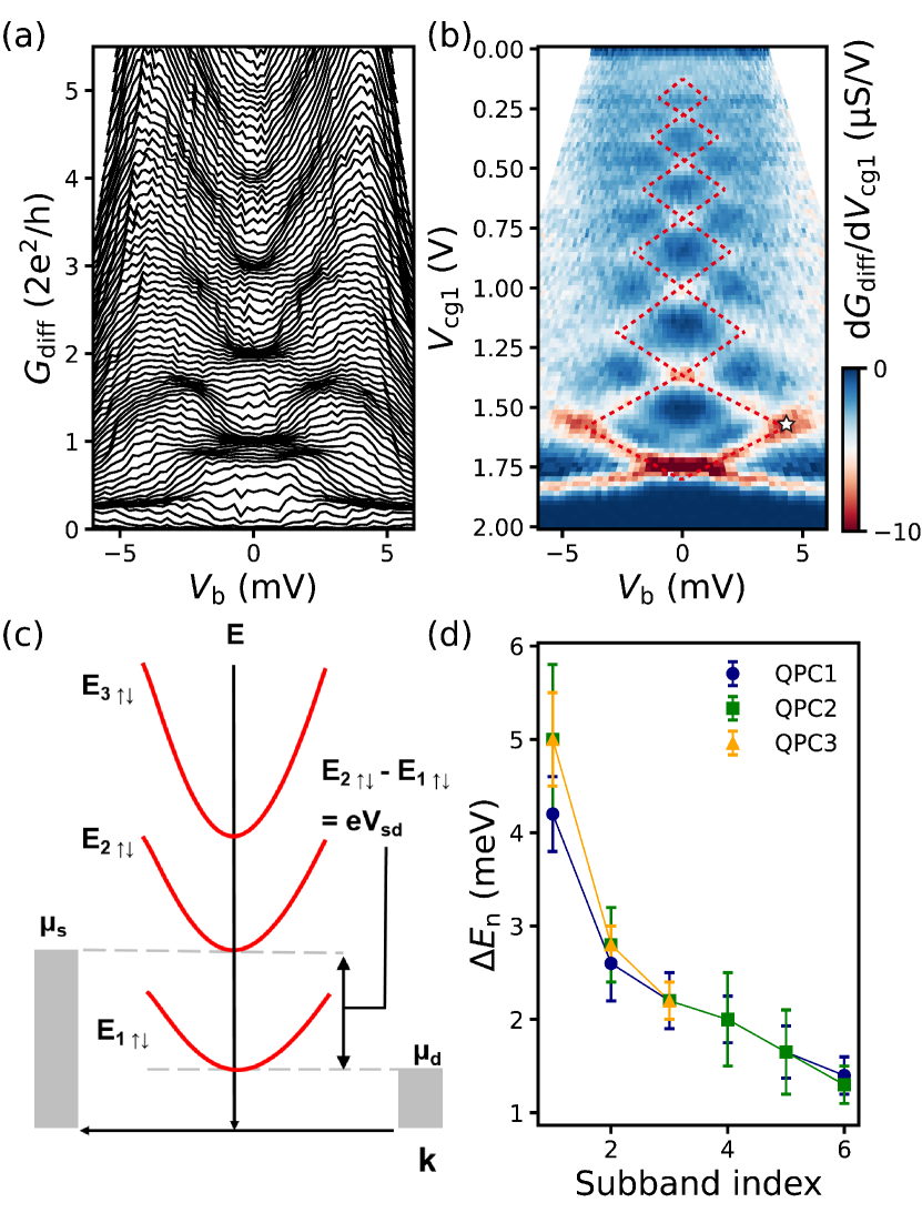
In the next, bias-spectroscopy measurements are employed to gain further insight into the energy scale of the gate-defined 1D subbands in the QPCs. In Figure 2, we perform bias-spectroscopy measurements on the QPCs in the absence of magnetic field and quantization energies between the 1D subbands are obtained. Figure 2(a) shows a waterfall plot of as a function of with varied for QPC1. In the plot, is varied from to with a step of and there is no offset between the traces. Dense regions correspond to conductance plateaus. At low , dense regions appear at integer multiples of as well as at . Half integer plateaus emerge at large when more than one subbands drops into the bias voltage window.Kouwenhoven et al. (1989); van Weperen et al. (2013) Then, we derive the conductance with respect to the constriction gate voltage and obtain transconductance d/d as a function of and [see Figure 2(b)]. In the figure, red dashed lines denote six consecutive diamonds implying that the first six 1D subbands are well separated in energy. Another set of faint diamond appears inside the bottom diamond which is a result of the anomaly.Kouwenhoven et al. (1989) Then, we perform analogous bias-spectroscopy measurements on QPC2 and QPC3 as shown in Figure S4 in the Supplementary Materials. With such spectroscopy measurements, quantization energies of 1D subbands can be extracted. Figure 2(c) shows the energy diagram of the subbands at a finite [star point in Figure 2(b)]. Each red parabola corresponds to a spin-degenerated 1D subband with subband index (). The chemical potential difference (also ) just matches the energy spacing between the first and second subband, denoted as , and the energy spacing is then extracted. Similarly, energy spacing depending on index is obtained for the three QPCs and corresponding results are displayed in Figure 2(d). We see that decreases with , which can be explained by a modulated QPC confinement potential profile with constriction gates. Populating more subbands needs more negative and thus reduces the curvature of the confinement potential, leading to smaller quantization energies of the subbands with larger indices. By adopting a harmonic potential for constriction gate confinement, the extension length of the confinement for a subband can be estimated as Hsueh et al. (2022)
| (1) |
where Kong et al. (2023) is the effective mass of the holes, is the angular frequency, and is the effective length of the lateral confinement for the th subband. With Eq. (1), the values for the first six subbands of QPC1 is estimated to be 13, 30, 42, 52, 64 and 77, respectively. The values of for the other two QPCs are provided in Figure S4 in the Supplementary Materials. Thus, the effective length of the first several subbands of the QPCs ranges from 12 to 80, smaller than the physical separations between the constriction gates in pairs (). Notably, the three QPCs have similar quantization energies as a function of the subband index, indicating a comparable gate confinement and a good reproducibility in device fabrication.
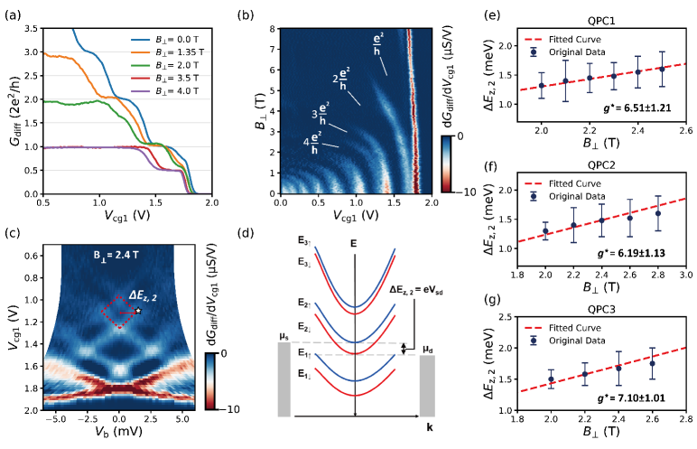
In the following, we focus on spin dependent behaviors of the QPCs subjected to perpendicular magnetic fields . Figure 3(a) displays zero-bias of QPC1 as a function of at several selected . At (blue trace), conductance plateaus appear mainly at integer multiples of . Due to the Zeeman effect, conductance shoulders at half integer of emerge from and the half integer plateaus become well visible at . Figure 3(b) presents transconductance d/d as a function of and . A large absolute value of d/d represents that a spin-degenerate or spin-indegenerate subband gets populated with decreasing the constriction gate voltage . With increasing , we see that the subbands get splitted in energy and spin-indegenerate subbands are obtained. Except for the Zeeman effect, has another influence that all subbands bend to low gate voltages due to the orbital effectLei et al. (2021); Mizokuchi et al. (2018); Ferry, Goodnick, and Bird (2009). This influence is more prominent for high-index subbands and these subbands are depopulated by the magnetic field even before a visible Zeeman splitting commences. Therefore, Zeeman effect on the QPCs is only observable for low-index subbands. In order to obtain Zeeman energies of the subbands, we conduct bias-spectroscopy measurements on QPCs at finite . Figure 3(c) shows d/d as a function of and at . Compared with Figure 2(b) (), spin-splitted subbands become visible in Figure 3(c). Red dashed lines denote the boundary of the diamond formed by the second subband with a finite Zeeman energy. Then, the Zeeman energy of the second subband can be extracted at . Figure 3(d) depicts the energy diagram of the spin-splitted subbands at finite [star point in Figure 3(c)]. Blue parabolas correspond to subbands with spin-up species and red parabolas are for spin-down subbands. Here, the chemical potential difference (also ) just equals the Zeeman splitting of the second subband . A series of measurements as in Figure 3(c) at different are performed for QPC1 (see Figure S5 in the Supplementary Materials) and Zeeman energies extracted at different are shown in Figure 3(e). Similar measurements have been done on QPC2 and QPC3, and corresponding results are shown in Figure S6 and S7 in the Supplementary Materials. Extracted Zeeman splittings of QPC2 and QPC3 as a function of are displayed in Figure 3(f) and 3(g), respectively. In Figures 3(e)-3(g), we make linear fits to the data (red dashed lines) and Landé factors of the second subband for the three QPCs are obtained. The extracted Landé factors are , consistent with previous reports on Ge hole gases.Sammak et al. (2019); Mizokuchi et al. (2018); Kong et al. (2023) Note that we only deal with Zeeman energy of the second subband because Zeeman splitting of the first subband is influenced by the anomaly (see Figure S5-S7) and higher subbands do not have visible splitting before being fully depopulated by .
In conclusion, we have experimentally studied QPCs defined in a Ge quantum well with electric gates. At zero magnetic field, we observe conductance plateaus at quantized values for all three QPCs, indicating a ballistic charge transport through 1D subbands. Bias-spectroscopy measurements are employed on the QPCs to obtain quantization energies between the subbands. The value varies with subband index from 1.5 to 5 as a consequence of modulated gate confinements. After that, the QPCs are studied in perpendicular magnetic fields and we observe splitted subbands in energy due to the Zeeman effect. With the extracted Zeeman splitting at different magnetic fields, Landé factors are obtained to be . Importantly, all three QPCs in the same device have uniform performances with regard to their lateral gate confinements and Landé factors. The uniformity is a key issue for constructing complex quantum devices with basic nanostructures. We therefore believe that our work is essentially important for pursuing Ge-based quantum technology in devices using QPC structures as a building block.
Acknowledgements.
This work is supported by the National Natural Science Foundation of China (Grants No. 12374480, 92165208, 11874071 and 92365103), and Innovation Program for Quantum Science and Technology (Project ID. 2021ZD0302301).conflict of interest
The authors declare no conflict of interests.
data availability
The data that support the findings of this study are available from the corresponding authors upon reasonable request.
References
- Scappucci et al. (2021) G. Scappucci, C. Kloeffel, F. A. Zwanenburg, D. Loss, M. Myronov, J.-J. Zhang, S. D. Franceschi, G. Katsaros, and M. Veldhorst, Nat. Rev. Mater. 6, 926–943 (2021).
- Bulaev and Loss (2007) D. V. Bulaev and D. Loss, Phys. Rev. Lett. 98, 097202 (2007).
- Moriya et al. (2014) R. Moriya, K. Sawano, Y. Hoshi, S. Masubuchi, Y. Shiraki, A. Wild, C. Neumann, G. Abstreiter, D. Bougeard, T. Koga, and T. Machida, Phys. Rev. Lett. 113, 086601 (2014).
- Li et al. (2018) Y. Li, S.-X. Li, F. Gao, H.-O. Li, G. Xu, K. Wang, D. Liu, G. Cao, M. Xiao, T. Wang, J.-J. Zhang, G.-C. Guo, and G.-P. Guo, Nano Lett. 18, 2091–2097 (2018).
- Tosato et al. (2023) A. Tosato, V. Levajac, J.-Y. Wang, C. J. Boor, F. Borsoi, M. Botifoll, C. N. Borja, S. Martí-Sánchez, J. Arbiol, A. Sammak, M. Veldhorst, and G. Scappucci, Commun. Mater. 4, 23 (2023).
- Watzinger et al. (2018) H. Watzinger, J. Kukuc̆ka, L. Vukus̆ić, F. Gao, T. Wang, F. Schäffler, J.-J. Zhang, and G. Katsaros, Nat. Commun. 9, 3902 (2018).
- Hendrickx et al. (2020a) N. W. Hendrickx, W. I. L. Lawrie, L. Petit, A. Sammak, G. Scappucci, and M. Veldhorst, Nat. Commun. 11, 3478 (2020a).
- Hendrickx et al. (2020b) N. W. Hendrickx, D. P. Franke, A. Sammak, G. Scappucci, and M. Veldhorst, Nature 577, 487 (2020b).
- Hendrickx et al. (2021) N. W. Hendrickx, W. I. L. Lawrie, M. Russ, F. van Riggelen, S. L. de Snoo, R. N. Schouten, A. Sammak, G. Scappucci, and M. Veldhorst, Nature 591, 580 (2021).
- Froning et al. (2021) F. N. M. Froning, L. C. Camenzind, O. A. H. van der Molen, A. Li, E. P. A. M. Bakkers, D. M. Zumbühl, and F. R. Braakman, Nat. Nanotechnol. 16, 308–312 (2021).
- Jirovec et al. (2021) D. Jirovec, A. Hofmann, A. Ballabio, P. M. Mutter, G. Tavani, M. Botifoll, A. Crippa, J. Kukucka, O. Sagi, F. Martins, J. Saez-Mollejo, I. Prieto, M. Borovkov, J. Arbiol, D. Chrastina, G. Isella, and G. Katsaros, Nat. Mater. 20, 1106–1112 (2021).
- Jirovec et al. (2022) D. Jirovec, P. M. Mutter, A. Hofmann, A. Crippa, M. Rychetsky, D. L. Craig, J. Kukucka, F. Martins, A. Ballabio, N. Ares, D. Chrastina, G. Isella, G. Burkard, and G. Katsaros, Phys. Rev. Lett. 128, 126803 (2022).
- Wang et al. (2022) K. Wang, G. Xu, F. Gao, H. Liu, R.-L. Ma, X. Zhang, Z. Wang, G. Cao, T. Wang, J.-J. Zhang, D. Culcer, X. Hu, H.-W. Jiang, H.-O. Li, G.-C. Guo, and G.-P. Guo, Nat. Commun. 13, 206 (2022).
- Ridderbos et al. (2020) J. Ridderbos, M. Brauns, F. K. de Vries, J. Shen, A. Li, S. Kölling, M. A. Verheijen, A. Brinkman, W. G. van der Wiel, E. P. A. M. Bakkers, and F. A. Zwanenburg, Nano Lett. 20, 122–130 (2020).
- Borsoi et al. (2023) F. Borsoi, N. W. Hendrickx, V. John, M. Meyer, S. Motz, F. van Riggelen, A. Sammak, S. L. de Snoo, G. Scappucci, and M. Veldhorst, Nat. Nanotechnol. (2023).
- Lodari et al. (2022) M. Lodari, O. Kong, M. Rendell, A. Tosato, A. Sammak, M. Veldhorst, A. R. Hamilton, and G. Scappucci, Appl. Phys. Lett. 120, 122104 (2022).
- Kong et al. (2023) Z. Kong, Z. Li, G. Cao, J. Su, Y. Zhang, J. Liu, J. Liu, Y. Ren, H. Li, L. Wei, G.-P. Guo, Y. Wu, H. H. Radamson, J. Li, Z. Wu, H.-O. Li, J. Yang, C. Zhao, T. Ye, and G. Wang, ACS Appl. Mater. Interfaces 15, 28799–28805 (2023).
- Adelsberger et al. (2023) C. Adelsberger, H. F. Legg, D. Loss, and J. Klinovaja, Phys. Rev. B 108, 155433 (2023).
- Luethi et al. (2023) M. Luethi, H. F. Legg, K. Laubscher, D. Loss, and J. Klinovaja, Phys. Rev. B 108, 195406 (2023).
- Laubscher, Sau, and Sarma (2024) K. Laubscher, J. D. Sau, and S. D. Sarma, Phys. Rev. B 109, 035433 (2024).
- Hendrickx et al. (2018) N. Hendrickx, D. Franke, A. Sammak, M. Kouwenhoven, D. Sabbagh, L. Yeoh, R. Li, M. Tagliaferri, M. Virgilio, G. Capellini, G. Scappucci, and M. Veldhorst, Nat. Commun. 9, 2835 (2018).
- Hendrickx et al. (2019) N. W. Hendrickx, M. L. V. Tagliaferri, M. Kouwenhoven, R. Li, D. Franke, A. Sammak, A. Brinkman, G. Scappucci, and M. Veldhorst, Phys. Rev. B 99, 075435 (2019).
- Vigneau et al. (2019) F. Vigneau, R. Mizokuchi, D. C. Zanuz, X. Huang, S. Tan, R. Maurand, S. Frolov, A. Sammak, G. Scappucci, F. Lefloch, and S. D. Franceschi, Nano Lett. 19, 1023–1027 (2019).
- Aggarwal et al. (2021) K. Aggarwal, A. Hofmann, D. Jirovec, I. Prieto, A. Sammak, M. Botifoll, S. Martí-Sánchez, M. Veldhorst, J. Arbiol, G. Scappucci, J. Danon, and G. Katsaros, Phys. Rev. Research 3, L022005 (2021).
- Valentini et al. (2024) M. Valentini, O. Sagi, L. Baghumyan, T. de Gijsel, J. Jung, S. Calcaterra, A. Ballabio, J. A. Servin, K. Aggarwal, M. Janik, T. Adletzberger, R. S. Souto, M. Leijnse, J. Danon, C. Schrade, E. P. A. M. Bakkers, D. Chrastina, G. Isella, and G. Katsaros, Nat. Commun. 15, 169 (2024).
- Fornieri et al. (2019) A. Fornieri, A. M. Whiticar, F. Setiawan, A. C. C. D. E. Portolés, A. Keselman, S. Gronin, C. Thomas, T. Wang, R. Kallaher, G. C. Gardner, E. Berg, M. J. Manfra, A. Stern, C. M. Marcus, and F. Nichele, Nature 569, 89–92 (2019).
- van der Wiel et al. (2002) W. G. van der Wiel, S. D. Franceschi, J. M. Elzerman, T. Fujisawa, S. Tarucha, and L. P. Kouwenhoven, Rev. Mod. Phys. 75, 1 (2002).
- Hanson et al. (2007) R. Hanson, L. P. Kouwenhoven, J. R. Petta, S. Tarucha, and L. M. K. Vandersypen, Rev. Mod. Phys. 79, 1217 (2007).
- Elzerman et al. (2004) J. M. Elzerman, R. Hanson, L. H. W. van Beveren, B. Witkamp, L. M. K. Vandersypen, and L. P. Kouwenhoven, Nature 430, 431–435 (2004).
- Bartolomei et al. (2020) H. Bartolomei, M. Kumar, R. Bisognin, A. Marguerite, J.-M. Berroir, E. Bocquillon, B. Plaçais, A. Cavanna, Q. Dong, U. Gennser, Y. Jin, and G. Fève, Science 368, 173–177 (2020).
- Nakamura et al. (2020) J. Nakamura, S. Liang, G. C. Gardner, and M. J. Manfra, Nat. Phys. 16, 931–936 (2020).
- Nakamura et al. (2023) J. Nakamura, S. Liang, G. C. Gardner, and M. J. Manfra, Phys. Rev. X 13, 041012 (2023).
- van Wees et al. (1988) B. J. van Wees, H. van Houten, C. W. J. Beenakker, J. G. Williamson, L. P. Kouwenhoven, D. van der Marel, and C. T. Foxon, Phys. Rev. Lett. 60, 848 (1988).
- Wharam et al. (1988) D. A. Wharam, T. J. Thornton, R. Newbury, M. Pepper, H. Ahmed, J. E. F. Frost, D. G. Hasko, D. C. Peacock, D. A. Ritchie, and G. A. C. Jones, J. Phys. C: Solid State Phys. 21, L209 (1988).
- Debray et al. (2009) P. Debray, S. M. S. Rahman, J. Wan, R. S. Newrock, M. Cahay, A. T. Ngo, S. E. Ulloa, S. T. Herbert, M. Muhammad, and M. Johnson, Nat. Nanotechnol. 4, 759 (2009).
- Mittag et al. (2019) C. Mittag, M. Karalic, Z. Lei, C. Thomas, A. Tuaz, A. T. Hatke, G. C. Gardner, M. J. Manfra, T. Ihn, and K. Ensslin, Phys. Rev. B 100, 075422 (2019).
- Lee et al. (2019) J. S. Lee, B. Shojaei, B. Shojaei, M. Pendharkar, A. P. McFadden, Y. Kim, H. J. Suominen, M. Kjaergaard, F. Nichele, H. Zhang, C. M. Marcus, and C. J. Palmstrøm, Nano Lett. 19, 3083–3090 (2019).
- Hsueh et al. (2022) C. L. Hsueh, P. Sriram, T. Wang, C. Thomas, G. Gardner, M. A. Kastner, M. J. Manfra, and D. Goldhaber-Gordon, Phys. Rev. B 105, 195303 (2022).
- Qu et al. (2016) F. Qu, J. van Veen, F. K. de Vries, A. J. A. Beukman, M. Wimmer, W. Yi, A. A. Kiselev, B.-M. Nguyen, M. Sokolich, M. J. Manfra, F. Nichele, C. M. Marcus, and L. P. Kouwenhoven, Nano Lett. 12, 7509–7513 (2016).
- Lei et al. (2021) Z. Lei, C. A. Lehner, E. Cheah, C. Mittag, M. Karalic, W. Wegscheider, K. Ensslin, and T. Ihn, Phys. Rev. Research 3, 023042 (2021).
- Gul et al. (2017) Y. Gul, S. N. Holmes, P. J. Newton, D. J. P. Ellis, C. Morrison, M. Pepper, C. H. W. Barnes, and M. Myronov, Appl. Phys. Lett. 111, 233512 (2017).
- Mizokuchi et al. (2018) R. Mizokuchi, R. Maurand, F. Vigneau, M. Myronov, and S. D. Franceschi, Nano Lett. 18, 4861–4865 (2018).
- Gul et al. (2018) Y. Gul, S. N. Holmes, M. Myronov, S. Kumar, and M. Pepper, J. Phys.: Condens. Matter 30, 09LT01 (2018).
- Cronenwett et al. (2002) S. M. Cronenwett, H. J. Lynch, D. Goldhaber-Gordon, L. P. Kouwenhoven, C. M. Marcus, K. Hirose, N. S. Wingreen, and V. Umansky, Phys. Rev. Lett. 88, 226805 (2002).
- Kouwenhoven et al. (1989) L. P. Kouwenhoven, B. J. van Wees, C. J. P. M. Harmans, J. G. Williamson, H. van Houten, C. W. J. Beenakker, C. T. Foxon, and J. J. Harris, Phys. Rev. B 39, 8040(R) (1989).
- van Weperen et al. (2013) I. van Weperen, S. R. Plissard, E. P. A. M. Bakkers, S. M. Frolov, and L. P. Kouwenhoven, Nano Lett. 13, 387–391 (2013).
- Ferry, Goodnick, and Bird (2009) D. K. Ferry, S. M. Goodnick, and J. Bird, Transport in Nanostructures (Cambridge University Press, 2009).
- Sammak et al. (2019) A. Sammak, D. Sabbagh, N. W. Hendrickx, M. Lodari, B. P. Wuetz, A. Tosato, L. Yeoh, M. Bollani, M. Virgilio, M. A. Schubert, P. Zaumseil, G. Capellini, M. Veldhorst, and G. Scappucci, Adv. Funct. Mater. 29, 1807613 (2019).