Flux tunable graphene-based superconducting quantum circuits coupled to 3D cavity
Abstract
Correlation between transmon and its composite Josephson junctions (JJ) plays an important role in designing new types of superconducting qubits based on quantum materials. It is desirable to have a type of device that not only allows exploration for use in quantum information processing but also probing intrinsic properties in the composite JJs. Here, we construct a flux-tunable 3D transmon-type superconducting quantum circuit made of graphene as a proof-of-concept prototype device. This 3D transmon-type device not only enables coupling to 3D cavities for microwave probes but also permits DC transport measurements on the same device, providing useful connections between transmon properties and critical currents associated with JJ’s properties. We have demonstrated how flux-modulation in cavity frequency and DC critical current can be correlated under the influence of Fraunhofer pattern of JJs in an asymmetric SQUID. The correlation analysis was further extended to link the flux-modulated transmon properties, such as flux-tunability in qubit and cavity frequencies, with SQUID symmetry analysis based on DC measurements. Our study paves the way towards integrating novel materials for exploration of new types of quantum devices for future technology while probing underlying physics in the composite materials.
I I. Introduction
Josephson junction (JJ) is a key component in superconducting qubits. Apart from the commonly used Al/Al2O3/Al S-I-S junctions (I stands for insulator and S stands for superconductor), there is a growing interest in using S-N-S junctions (N stands for normal metals, but can also be semiconductors) as core components in superconducting qubits Kroll et al. (2018); Wang et al. (2019); Casparis et al. (2018); Hertel et al. (2022); Lo et al. (2023); Larsen et al. (2015); de Lange et al. (2015); Huo et al. (2023). Quantum materials, owing to their rich internal degrees of freedom unexplored, provide versatile functions to be integrated as a main ingredient in superconducting qubits Chiu and Xu (2017); Liu and Hersam (2019); Chiu (2020); Siddiqi (2021). Graphene and two-dimensional electron gas (2DEG), due to their 2D hence gate tunable natures, can serve as normal metals in S-N-S junctions, forming gate tunable transmons generally referred as gatemons Kroll et al. (2018); Wang et al. (2019); Casparis et al. (2018); Hertel et al. (2022); Lo et al. (2023). Semiconducting InAs nanowires can be similarly regarded and have been demonstrated as gatemons Larsen et al. (2015); de Lange et al. (2015); Huo et al. (2023) or resonator-type superconducting devices Hays et al. (2020, 2021). On the other hand, 2D materials such as NbSe2 have been used as superconductors in S-N-S junctions while hBN and MoS2 have been used as barrier layers in S-I-S junctions for transmon-type of devices Antony et al. (2021); Wang et al. (2022); Lee et al. (2019). Furthermore, using topological materials as the weak link in JJs may provide a different route to realizing the exotic Majorana bound states where 4-period phase modulation is expected Fu and Kane (2009). Therefore, with transmon architectures, one will be able to probe the topological nature of the composite topological Josephson junctions Chiu et al. (2020); Schmitt et al. (2022); Sun et al. (2023).
Transport measurements often provide fundamental information in probing JJ’s internal degrees of freedom, including conventional Andreev bound states (ABSs) and exotic Majorana modes, which are distinguished by 2 vs 4 periodic contributions to the supercurrent Badiane et al. (2013). However, due to its slow probing speed, it cannot access to dynamical probing and often suffers from quasiparticle poisoning, which tends to restore 4 periodic supercurrent to 2 periodicity in topological junctions Badiane et al. (2013); Sun et al. (2022). On the other hand, microwave technique used in superconductig qubits is a powerful tool that usually operates in the time scale of microseconds Krantz et al. (2020), fast enough to probe dynamic processes such as quasiparticle tunneling that often happens in the time scale between s and ms Rainis and Loss (2012); Karzig et al. (2021); Sun et al. (2022). Therefore, it is desirable to have a type of device that can not only allow transport measurement to reveal critical current information associated with ABSs, but also permits transmon-type microwave measurements for potential probing the dynamic properties of ABSs.
In this letter, we construct 3D transmon-type superconducting quantum circuits made of graphene as a proof-of-concept prototype device to address the aforementioned desires. This graphene-based superconducting quantum circuit consists of a pair of capacitor pads, which serve as the antenna to interact with microwave in a 3D copper cavity as well as for the bond pads in DC transport measurements. From both type of measurements, we find correlation between two approaches, which lay the foundations enabling exploration of new material-based quantum devices for future technology while probing underlying physics in the composite materials.
II II. Device fabrication and measurement setup
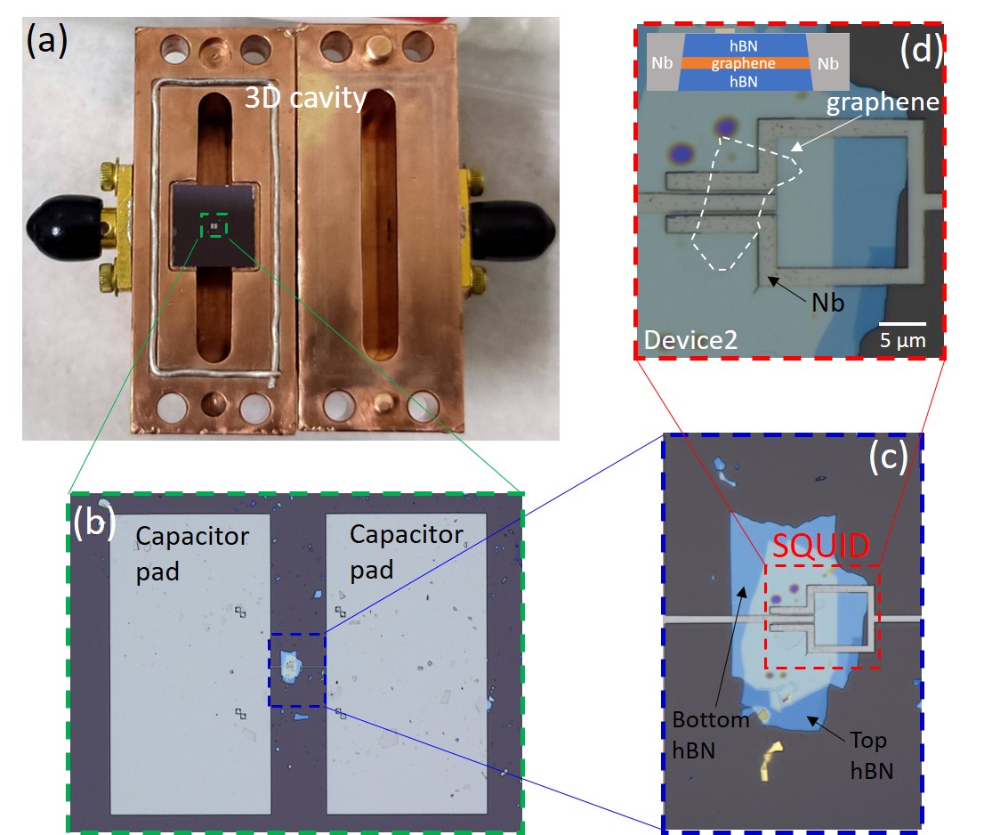
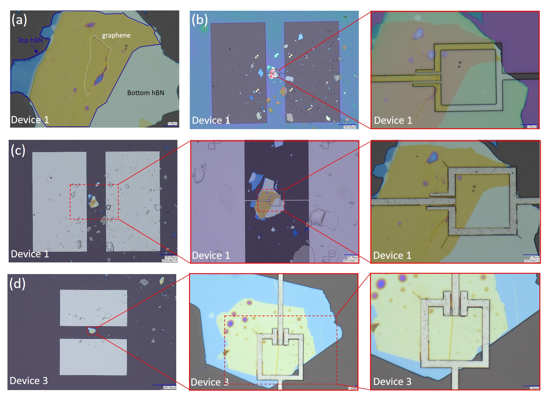
Fig. 1 shows the optical micrograph of our flux tunable graphene-based superconducting quantum circuits coupled to a 3D copper cavity. This transmon-type quantum circuit consists of a superconducting quantum interference device (SQUID) made of two Nb-Graphene-Nb junctions, with an enclosed loop of Nb at a nominal size of 16 16 [Fig. 1 (d)]. In order to preserve the graphene quality, the exfoliated graphene is encapsulated by hexagonal Boron Nitride (hBN) [Fig. 1 (c)], and the SQUID is fabricated based on the edge contact techniques Wang et al. (2013), as described in section I in Supplementary Materials (SM). The SQUID is shunted by a capacitor formed between two rectangular capacitor pads as shown in Fig. 1 (b), which effectively forms a transmon. In qubit type of microwave measurements, these two capacitor pads act as an antenna to interact with electromagnetic field in 3D cavities; while in DC transport measurements, these two capacitor pads are used as bond pads.
The measurement scheme for microwave and DC transport exploited in this work is illustrated in Fig. S3 (a) and (b), respectively. For microwave measurements, as shown in Fig. 1 (a), the devices were placed in a two-ports 3D copper cavity to provide good thermal conductivity and to allow externally applied magnetic fields to thread through the cavity for flux-tuning. Our 3D cavity is designed as a rectangular resonator, the resonance frequency of which is given by the formula: = , where , and represent the three-dimensional lengths of the rectangular resonator while , and represent the mode numbers. Generally, the transmon qubit placed in the center of the cavity chamber [Fig. 1 (a)] is primarily coupled with the electric field of TE101 mode Nguyen (2020). In this work, three devices labeled as 1, 2 and 3 were characterized, and they were placed in a 5.5 GHz (device 1 and 2) cavity and a 6.03 GHz (device 3) cavity for microwave measurements, respectively. For calibrating 3D cavities, performing transmission (S21) and DC transport measurements, please refer to section II in SM.
III III. Device characterization and results
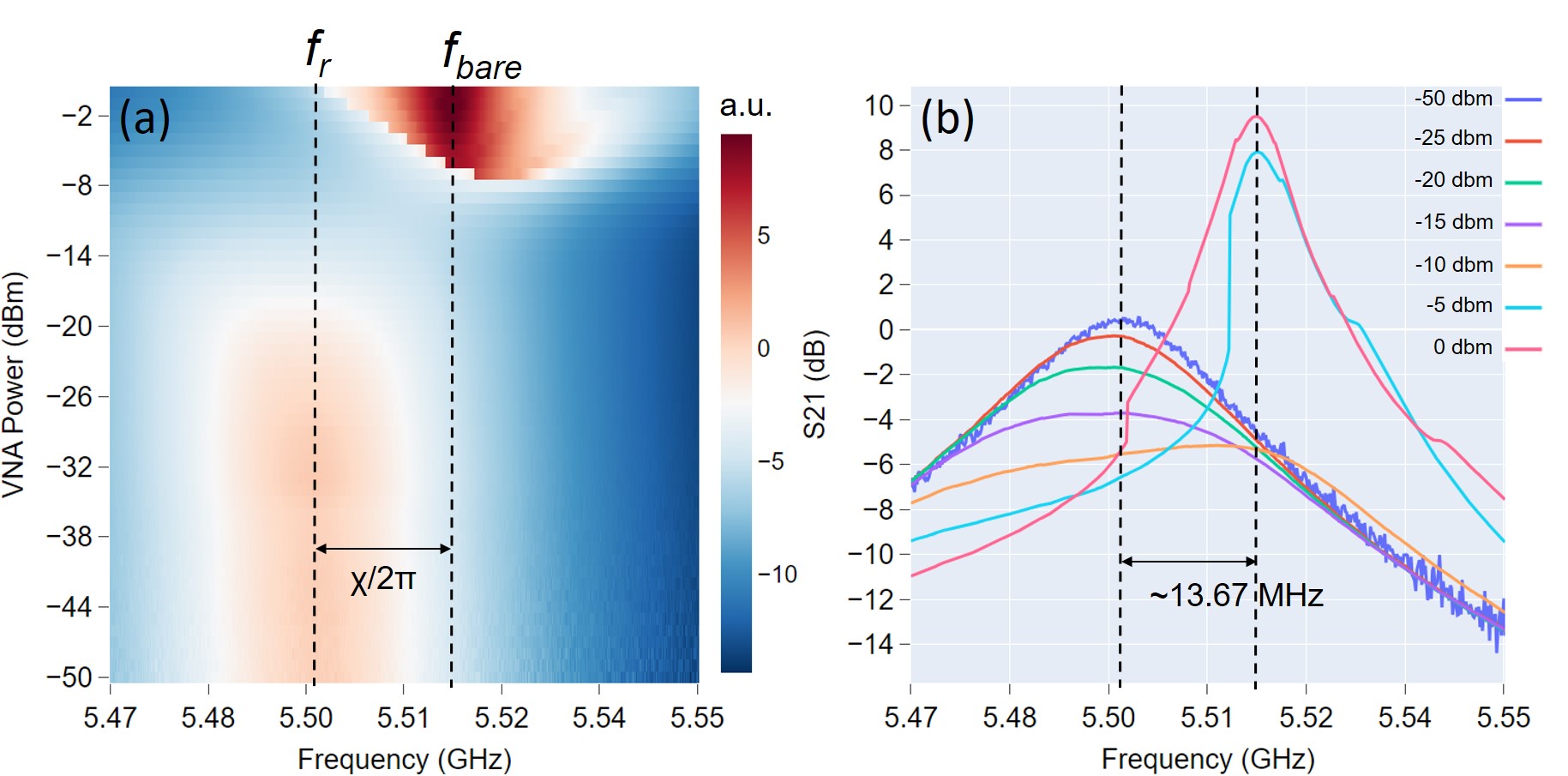
We first performed the qubit punch-out measurements on device 1, in which the transmission of the two-ports 3D cavity was measured S21 measurement of a vector network analyzer (VNA) as a function of readout power and frequency, as shown in Fig. 2(a). This is a conventional way to confirm the existence of JJ Reed et al. (2010), where the resonant frequency of the cavity () shifts toward the qubit frequency at large enough power around 0 dBm. Fig. 2(b) shows the linecuts at different readout powers. At lower powers from -50 dBm to -15 dBm, the cavity frequency centers around 5.5 GHz with an asymmetric line shape, indicating a canonical behavior of a Kerr-Duffing oscillator Reed (2014). After undergoing a broad range (-15 dBm P -8 dBm), the cavity response re-appears with a narrower line shape of Lorentzian and a frequency shifted to 5.516 GHz at P = 0 dBm, which is known as the bare cavity frequency () at which the cavity would resonate in the absence of JJs. The dispersive shift of around 13.67 MHz between cavity’s frequency at low power () and at high-power () allows us to estimate the qubit-cavity coupling strength and , where is qubit frequency. To deduce , we have performed two-tone measurements (data not shown), but no qubit transition was found in the probed frequency range of 4 to 12 GHz. Although we cannot obtain direct information about two-tone, we have relied on critical current in transport data to estimate both and , as discussed in section IV in SM.
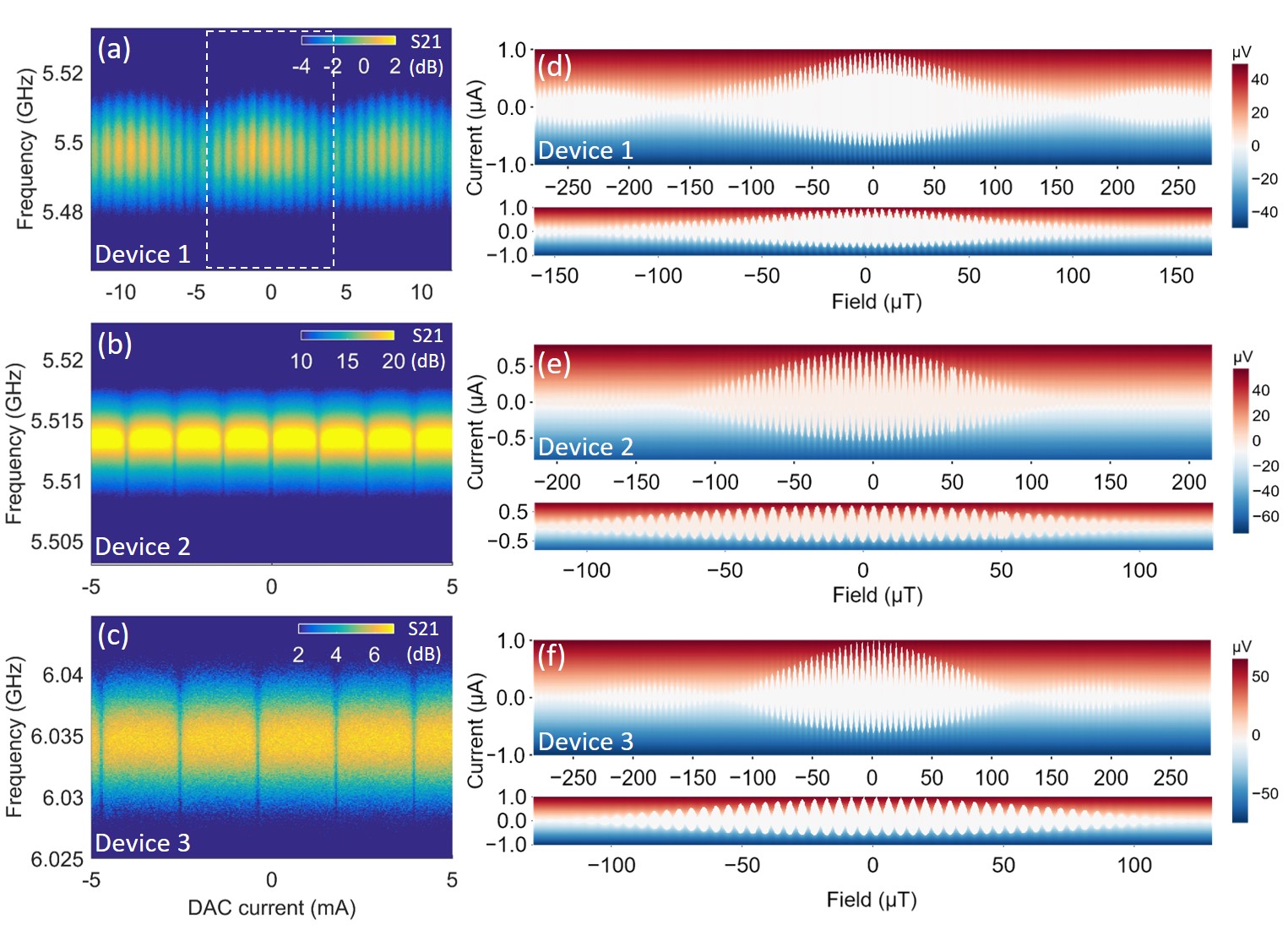
Microwave measurements of flux-tuning on graphene SQUID was executed by measuring the resonant cavity frequency at a low readout power (-55 dBm) while tuning the DC source current passing through the home-made superconducting coil around the cooper 3D cavity. The flux-modulated resonant cavity frequency for device 1, 2 and 3 is shown in Fig. 3(a), (b) and (c), respectively. Interestingly, while a periodic modulation of cavity frequency was observed in device 2 and 3 [Fig. 3(b) and (c)], as being commonly seen in conventional AlAl2O3-based transmons Chow (2010), there is an additional larger-period flux modulation observed in device 1, as indicated by the dashed box in Fig. 3(a). This larger-period modulation is superimposed on a fine modulation presumably from SQUID critical current oscillation, with a ratio of 10 to 1 in period. We attribute this additional modulation to the Fraunhofer oscillation resulted from the composing graphene JJs (section III in SM). In a symmetric SQUID whose interference pattern is modulated by the Fraunhofer diffraction patterns of each JJ, the total critical current can be described as Qu et al. (2012):
| (1) |
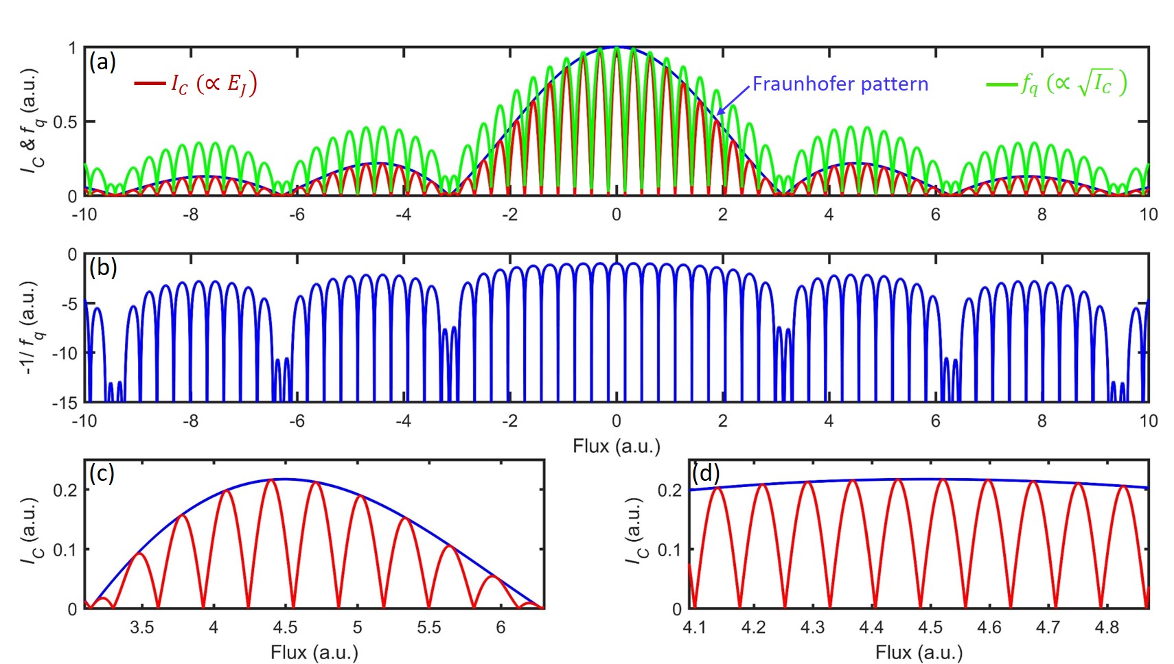
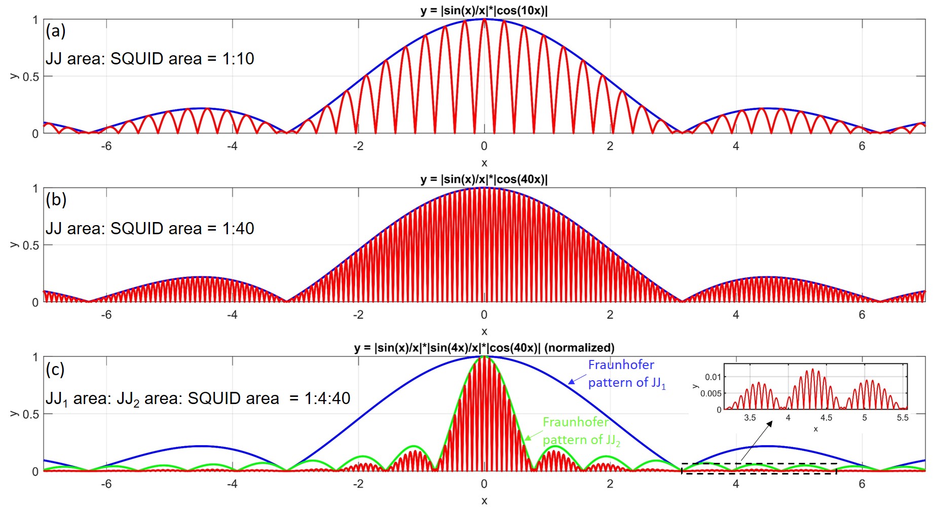
where is the critical current of each junction at zero magnetic field, is the flux threading through the single junction area, is the flux threading through the loop area of SQUID and = is the flux quanta. The first term in equation 1 represents the Fraunhofer pattern which consists of a central lobe and a series of sub-lobes, while the second term represents SQUID oscillations. The ratio between the SQUID loop area and JJ area determines how many SQUID oscillations reside in a lobe of Fraunhofer pattern. The central lobe in Fraunhofer pattern contains twice the number of SQUID oscillations in other sub-lobes. The modulation behavior of equation 1 with respect to the applied flux is illustrated in Fig. 4(a), with the SQUID loop area set to be 10 times of the junction area, to emulate the situation observed in Fig. 3(a) [see detailed discussions in section III of SM]. As can be seen in Fig. 4(a), the Fraunhofer pattern indicated by the blue solid lines is modulating the SQUID critical current oscillations indicated by the red solid lines. We can relate the Fraunhofer effect-mediated SQUID critical current with different transmon’s parameters. Since Josephson energy = is proportional to while qubit frequency is proportional to , their flux modulation under Fraunhofer effect is shown in red and green solid lines in Fig. 4(a), respectively. By controlling the magnetic flux threading through the SQUID loop, we are able to modify the critical current, hence and , which leads to different dispersive shift to be measured in cavity frequency. In Fig. 4(b), we show the schematically simulated dispersive shift under the influence of Fraunhofer effect (see discussions in section III of SM). Due to the effect of square root and reciprocal, the large variation in height of Fraunhofer lobes [blues curve in Fig. 4(a)] has become a relatively small variation in dispersive shift as shown in Fig. 4(b).
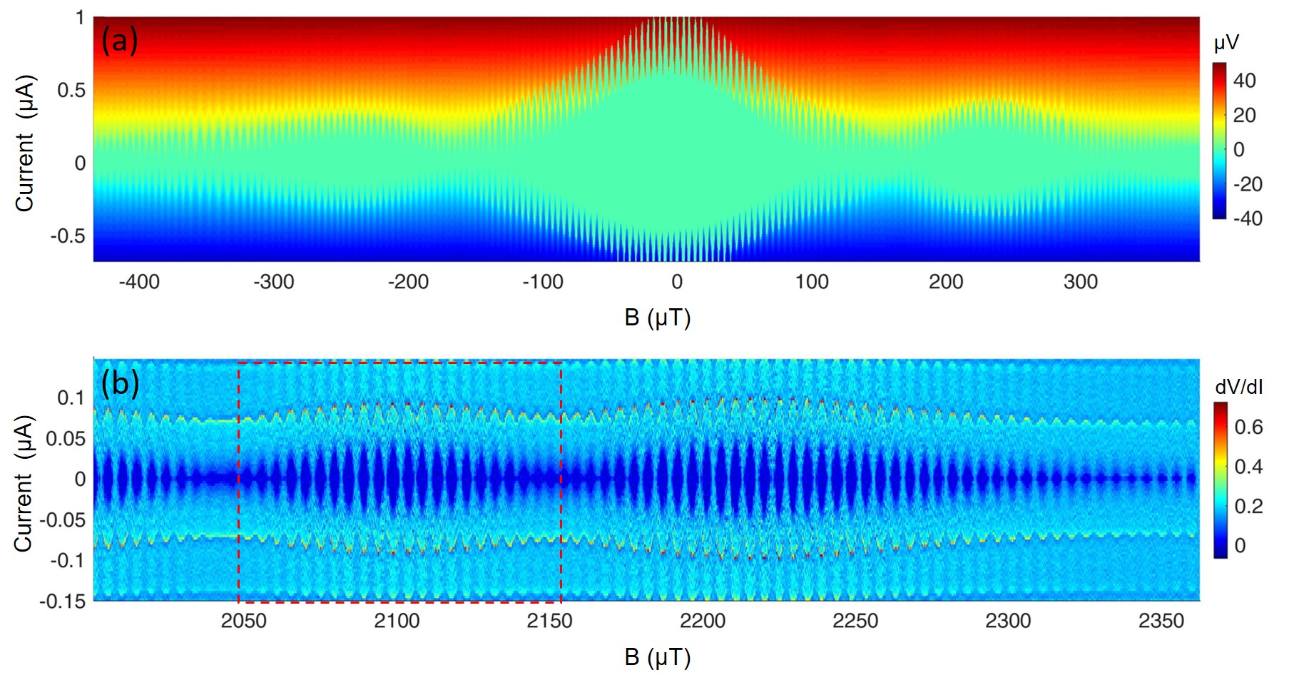
In order to gain more insight into how critical current is correlated with the microwave measurement of our graphene-based quantum circuits, we have performed DC transport measurements on device 1, 2 and 3, as shown in Fig. 3(d), (e) and (f), respectively. All devices have shown the SQUID modulations with Fraunhofer pattern, with 82 oscillations in the central lobe for device 1, 61 oscillations in that for device 2 and 55 oscillations in that for device 3 [bottom panels of Fig. 3(d), (e) and (f)]. Notably, for device 1, Fig. 3(d) indicates that the number of SQUID oscillations in the Fraunhofer sub-lobe is 41, which is four times of the number 10 observed in the microwave measurement shown in Fig. 3(a). One possible reason for the periods’ ratio discrepancy between microwave and DC measurements is due to different cool down. While the sample moved from one setup to another, the junction degradation may lead to a change in the ratio between the Fraunhofer period and the SQUID period. However, in later analysis, we found that SQUID’s JJs in device 1 are asymmetric with a ratio : = 1:4, which coincides with the above ratio 10:41 comparing microwave with DC results. Thus, we attribute the Fraunhofer modulation observed in microwave measurement to the larger junction in the asymmetric SQUID, with a area ratio to SQUID loop 1:10 as indicated by JJ2 in Fig. S4(c) (see discussions in section III of SM).
The Fraunhofer pattern modulation was not pronounced in the microwave measurements of device 2 [Fig. 3(b)] and device 3 [Fig. 3 (c)], while the transport data as shown in Fig. 3(e) and Fig. 3(f) present Fraunhofer modulation with the central lobes containing large number of SQUID oscillations (61 for device 2 and 55 for device 3). This can be understood as illustrated in Fig. S4 (a) and (b), where different ratio of area between junction to SQUID loop leads to 10 and 40 SQUID oscillations residing in a Fraunhofer sub-lobe, respectively. Thus, if we compare 10 SQUID oscillations in each case, the Fraunhofer modulation on SQUID oscillations is more pronounced in large SQUID loop-to-junction area ratio, as illustrated in Fig. 4(c) and (d), respectively (we used 40 SQUID oscillations as an example but the same concept apply to the case of device 2 and device 3). In addition, we note that the heights of the three Fraunhofer sub-lobes observed in Fig. 3(a) are similar (around 5.52 GHz). We speculate that these sub-lobes from JJ2 do not reside in the strong-modulating central lobe of the smaller junction (JJ1), but locate in JJ1’s outer sub-lobe as shown in the inset of Fig. S4(c), possibly due to the remanent magnetic field in our superconducting coil. In a similar regard, the flux modulation shown in Fig. 3(b) and Fig. 3 (c) also origin from the outer Fraunhofer sub-lobes, which has less modulation on SQUID oscillations compared to that in the central lobe, as evident in the transport data shown in Fig. 3(e) and Fig. 3 (f).
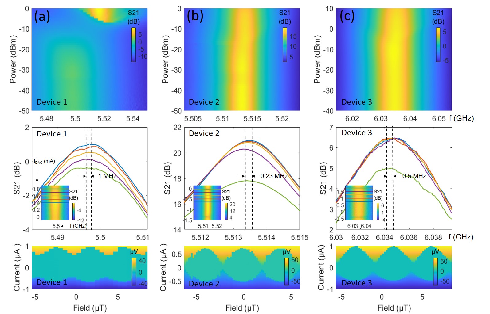
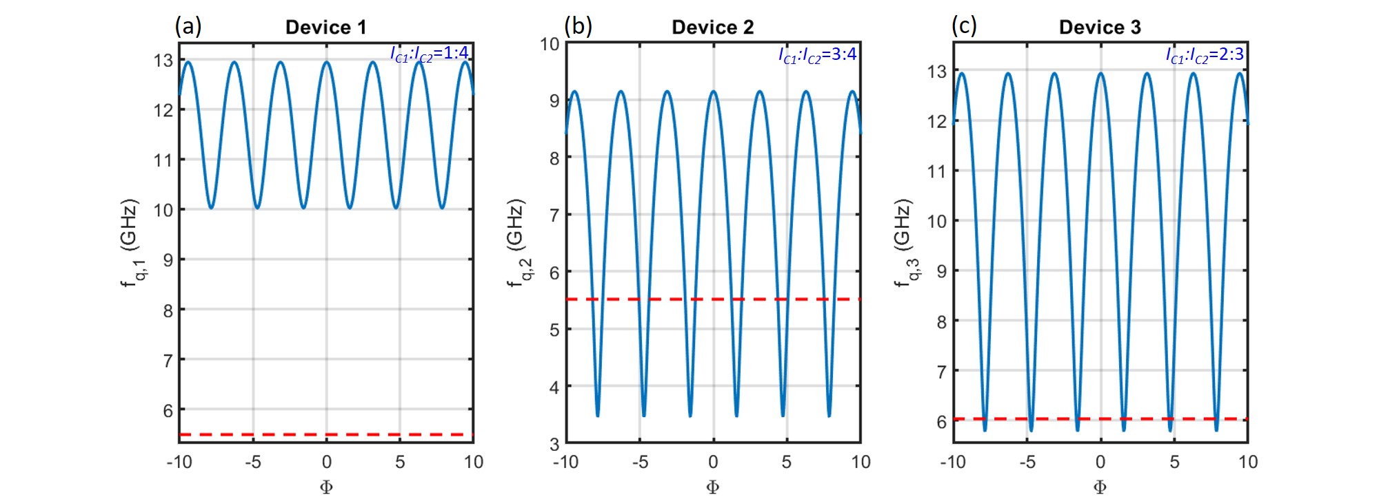
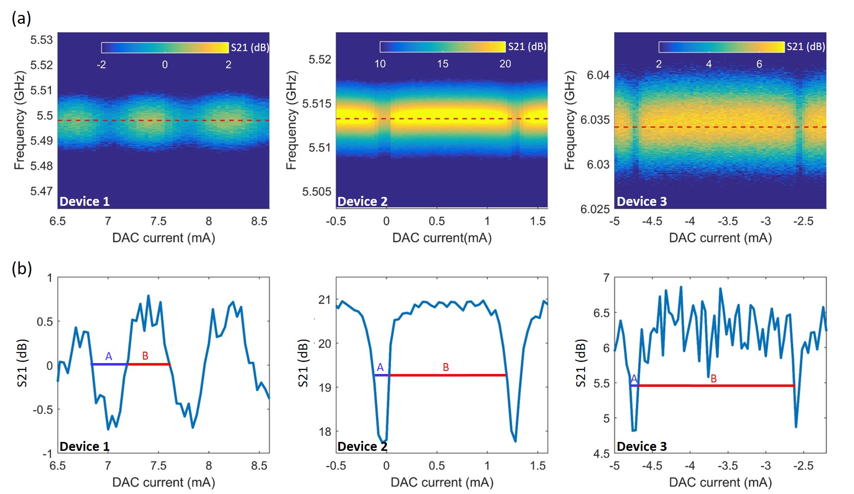
In order to find more correlations between transport and transmon-type measurements, we further compare the qubit punch-out, flux-tunability of cavity frequency and DC critical current of SQUID for three devices, as shown in Fig. 5. In the top panels of Fig. 5, the dispersive shift is 13.67 MHz, 0.48 MHz and 0.68 MHz for device 1, 2 and 3, respectively; while in the middle panels the maximal flux-tunability of cavity frequency is 1 MHz, 0.23 MHz and 0.5 MHz for device 1, 2 and 3, respectively. In section IV of SM, we have estimated the qubit-cavity coupling strength based on the SQUID critical current in the sub-lobe of Fraunhofer pattern. The estimated for device 2 and 3 are small as 41.76 MHz and 68.5 MHz, which can account for the relatively small flux-tunability. However, the estimated for device 1 is relatively large (318.9 MHz) while the flux-tunability is still small, and if the qubit frequency intersect with cavity frequency, a large Rabi splitting is expected, which was not observed in the middle panel of Fig. 5 (a). We attribute this to the asymmetry of the SQUID in device 1 as compared to device 2 and device 3, as revealed in the bottom panels of Fig. 5, which show three SQUID critical current oscillations for each device. The asymmetry of the SQUID and the resulting skewed current phase relation (CPR) have been studied in graphene and InAs junctions before Thompson et al. (2017); Mayer et al. (2020). It has been shown that the asymmetry in the SQUID inductance () and JJs () will both account for the distorting nonsinusoidal SQUID oscillations, while the minimum value of SQUID critical current only depends on the JJs asymmetry () Clarke (2004). With increasing , increases, leading to a reduction of modulation depth of SQUID critical current ()/, where is the average critical current of the two junctions Clarke (2004). This situation can be clearly observed in the bottom panels of Fig. 5, where around 0.6 A for device 1 is higher compared to that for device 2 and 3 around 0.1 A and 0.2 A, leading to a smaller modulation depth of SQUID critical current in device 1 as compared to device 2 and 3. This indicates a highly asymmetric SQUID in device 1 as compared to device 2 and 3 (also see relevant discussions in section V of SM). The transmons made of SQUID with asymmetric JJs have been investigated before in ref. Krantz et al. (2020). The modulation of with applied flux in such a transmon is described by = , where = + and = ( 1)/( + 1) is the junction asymmetry parameter, with = / (subscript 1 and 2 denote the JJ index) Krantz et al. (2020). A large junction asymmetry parameter will result in qubit frequency oscillating at its maximal frequency with suppressed flux sensitivity (see section V in SM). As shown in Fig. S7 (a), the qubit frequency for device 1 oscillating between 12.935 GHz and 10.02 GHz is well above without intercepting with the cavity frequency around 5.5 GHz, leading to the small flux-tunability in cavity frequency even with a large qubit-cavity coupling strength . In contrast, the SQUIDs are more symmetric in device 2 and 3, in which qubit frequency oscillation intersects with cavity frequency around 5.5 GHz and 6 GHz, as shown in Fig. S7 (b) and (c), respectively. We find supports to our simulations (Fig. S7) in our flux-modulated cavity frequency data as shown in Fig. 6. Fig. 6 (a) shows the flux modulation of cavity frequency for all three devices while Fig. 6 (b) shows the corresponding linecuts along the dashed lines in Fig. 6 (a). Since intersect with cavity frequency around the central position while intersect with cavity frequency in a lower position in modulation as shown in Fig. S7 (b) and (c), one can expect that the ratio between the flux regions where and is different in two devices. This can be clearly observed in Fig. 6 (b), where the ratio between the length of line A (denoting the region where ) and line B (denoting the region where ) is larger in device 2 as compared to that in device 3. In contrast, oscillates well above the cavity frequency as shown in Fig. S7 (a), we expect the up-and-down modulation of will reflect on that in cavity frequency similarly. This is also observed in the left panel of Fig. 6 (b), where the ratio between the length of line A and B is close to unity.
The estimated is 83.5 MHz for device 2 and 137 MHz for device 3, indicating that an exchange of energy between qubit and cavity would occur with a period of 11.97 ns in device 2 and 7.3 ns in device 3, respectively. The fact that the avoided crossing was not observed in flux-tuning data [Fig. 3 (b) and (c)] implies the qubit loses its coherence before a full round-trip exchange of energy can occur between the qubit and the cavity (see section IV of SM). The coherence time of the qubit should be roughly two or three times longer to see a well-formed avoided crossing. This implies an upper bound of coherence time 24 - 36 ns for device 2 and 14.6 - 22 ns for device 3, which is in a reasonable range within the coherence times reported from graphene 2D transmons Wang et al. (2019). In future endeavors, we anticipate by replacing SiSiO2 substrate with Si or sapphire substrates to reduce the dielectric loss, while adding magnetic shielding and infrared radiation filters, can further improve the decoherence time properties of the graphene-based quantum circuits in our systems Oliver and Welander (2013); O’Connell et al. (2008); Córcoles et al. (2011); Barends et al. (2011).
IV IV. Summary and prospect
In summary, we have demonstrated and characterized a series of flux tunable graphene-based superconducting quantum circuits based on 3D transmon architectures. We observed Fraunhofer pattern modulation in both cavity frequency (microwave measurements) and SQUID critical current oscillations (transport measurements) in one device, and found the correlation between the two can be associated with an asymmetric SQUID. We have provided a schematic to illustrate the flux-modulated supercurrent, qubit frequency and dispersive shift under the influence of Fraunhofer effect, which was used to connect with our microwave and transport data. We have relied on the DC critical current analysis to extract both the transmon-related parameters (, and ) and information of SQUID symmetry, which were later correlated with the flux-modulated transmon behavior in microwave measurements. Our device architectures enabling both DC and microwave probes can be extended to other quantum materials, where the unconventional ABSs play a role and result in topological phenomenon such as nontrivial 4-period supercurrent and qubit frequency Badiane et al. (2013); Sun et al. (2022). For example, one can first probe the missing n=1 Shapiro step in DC transport to reveal the possible existence of non-trivial 4-periodic ABSs Wiedenmann et al. (2016); Bocquillon et al. (2016); Li et al. (2018). The same device can then be placed in a 3D cavity to probe the 4 modulation of qubit frequency using time-domain spectroscopy, with the possibility to avoid quasiparticle poisoning. Our studies pave the way towards integrating novel materials for exploration of new types of quantum devices for future technology while probing underlying physics in the composite materials.
V V. Acknowledgments
Kuei-Lin Chiu would like to thank the funding support from National Science and Technology Council (Grant No. NSTC 109-2112-M-110-005-MY3 and NSTC 112-2112-M-110-017). Chung-Ting Ke and Yi-Chen Tsai would like to thank the funding support from National Science and Technology Council (Grant No. NSTC 110-2628-M-001-007). Kuei-Lin Chiu and Yen-Hsiang Lin also acknowledge support from the Center for Quantum Science and Technology (CQST) within the framework of the Higher Education Sprout Project by the Ministry of Education (MOE) in Taiwan.
Kuei-Lin Chiu would like to thank Valla Fatemi and Yueh-Nan Chen for the useful suggestions on the manuscript.
VI VI. Author contributions
K. L. Chiu conceived the project. Y. Chang fabricated the devices under the supervision of C. T. Ke. Y. H. Chen and A. J. Lasrado calibrated the 3D cavity with input from K. L. Chiu and Y. H. Lin. A. J. Lasrado performed the microwave measurements under the supervision of K. L. Chiu and with contributions from C. H. Lo, T. Y. Hsu and Y. C. Chen. Y. Chang performed the DC transport measurements under the supervision of C. T. Ke and with contributions from Y. C. Tsai. Samina and A. J. Lasrado performed the capacitance simulation under the supervision of Y. H. Lin. K. L. Chiu and C. T. Ke co-supervise the project.
VII VII. Competing financial interests
The authors declare no competing financial interests.
References
- Kroll et al. (2018) J. G. Kroll, W. Uilhoorn, K. L. van der Enden, D. de Jong, K. Watanabe, T. Taniguchi, S. Goswami, M. C. Cassidy, and L. P. Kouwenhoven, Nature Communications 9, 4615 (2018), ISSN 2041-1723, URL https://doi.org/10.1038/s41467-018-07124-x.
- Wang et al. (2019) J. I.-J. Wang, D. Rodan-Legrain, L. Bretheau, D. L. Campbell, B. Kannan, D. Kim, M. Kjaergaard, P. Krantz, G. O. Samach, F. Yan, et al., Nature Nanotechnology 14, 120 (2019), ISSN 1748-3395, URL https://doi.org/10.1038/s41565-018-0329-2.
- Casparis et al. (2018) L. Casparis, M. R. Connolly, M. Kjaergaard, N. J. Pearson, A. Kringhøj, T. W. Larsen, F. Kuemmeth, T. Wang, C. Thomas, S. Gronin, et al., Nature Nanotech 13, 915–919 (2018), URL https://doi.org/10.1038/s41565-018-0207-y.
- Hertel et al. (2022) A. Hertel, M. Eichinger, L. O. Andersen, D. M. van Zanten, S. Kallatt, P. Scarlino, A. Kringhøj, J. M. Chavez-Garcia, G. C. Gardner, S. Gronin, et al., Phys. Rev. Applied 18, 034042 (2022), URL https://journals.aps.org/prapplied/abstract/10.1103/PhysRevApplied.18.034042.
- Lo et al. (2023) C.-H. Lo, Y.-H. Chen, A. J. Lasrado, T. Kuo, Y.-Y. Chang, T.-Y. Hsu, Y.-C. Chen, G.-P. Guo, and K.-L. Chiu, SPIN p. 2340021 (2023), ISSN 2010-3247, URL https://doi.org/10.1142/S2010324723400210.
- Larsen et al. (2015) T. W. Larsen, K. D. Petersson, F. Kuemmeth, T. S. Jespersen, P. Krogstrup, J. Nygård, and C. M. Marcus, Phys. Rev. Lett. 115, 127001 (2015), URL https://link.aps.org/doi/10.1103/PhysRevLett.115.127001.
- de Lange et al. (2015) G. de Lange, B. van Heck, A. Bruno, D. J. van Woerkom, A. Geresdi, S. R. Plissard, E. P. A. M. Bakkers, A. R. Akhmerov, and L. DiCarlo, PRL 115, 127002 (2015), URL https://link.aps.org/doi/10.1103/PhysRevLett.115.127002.
- Huo et al. (2023) J. Huo, Z. Xia, Z. Li, S. Zhang, Y. Wang, D. Pan, Q. Liu, Y. Liu, Z. Wang, Y. Gao, et al., Chinese Physics Letters 40, 047302 (2023), ISSN 0256-307X, URL https://dx.doi.org/10.1088/0256-307X/40/4/047302.
- Chiu and Xu (2017) K.-L. Chiu and Y. Xu, Physics Reports 669, 1 (2017), ISSN 0370-1573, single-electron Transport in Graphene-like Nanostructures, URL //www.sciencedirect.com/science/article/pii/S0370157316303933.
- Liu and Hersam (2019) X. Liu and M. C. Hersam, Nature Reviews Materials 4, 669 (2019), ISSN 2058-8437, URL https://doi.org/10.1038/s41578-019-0136-x.
- Chiu (2020) K. L. Chiu, in 21st Century Nanoscience–A Handbook: Nanophotonics, Nanoelectronics, and Nanoplasmonics (CRC Press, 2020), pp. 13–1–13–48.
- Siddiqi (2021) I. Siddiqi, Nature Reviews Materials 6, 875 (2021), ISSN 2058-8437, URL https://doi.org/10.1038/s41578-021-00370-4.
- Hays et al. (2020) M. Hays, V. Fatemi, K. Serniak, D. Bouman, S. Diamond, G. de Lange, P. Krogstrup, J. Nygård, A. Geresdi, and M. H. Devoret, Nature Physics 16, 1103 (2020), ISSN 1745-2481, URL https://doi.org/10.1038/s41567-020-0952-3.
- Hays et al. (2021) M. Hays, V. Fatemi, D. Bouman, J. Cerrillo, S. Diamond, K. Serniak, T. Connolly, P. Krogstrup, J. Nygård, A. Levy Yeyati, et al., Science 373, 430 (2021), URL https://doi.org/10.1126/science.abf0345.
- Antony et al. (2021) A. Antony, M. V. Gustafsson, G. J. Ribeill, M. Ware, A. Rajendran, L. C. G. Govia, T. A. Ohki, T. Taniguchi, K. Watanabe, J. Hone, et al., Nano Lett. 21, 10122 (2021), ISSN 1530-6984, URL https://doi.org/10.1021/acs.nanolett.1c04160.
- Wang et al. (2022) J. I.-J. Wang, M. A. Yamoah, Q. Li, A. H. Karamlou, T. Dinh, B. Kannan, J. Braumüller, D. Kim, A. J. Melville, S. E. Muschinske, et al., Nature Materials 21, 398 (2022), ISSN 1476-4660, URL https://doi.org/10.1038/s41563-021-01187-w.
- Lee et al. (2019) K.-H. Lee, S. Chakram, S. E. Kim, F. Mujid, A. Ray, H. Gao, C. Park, Y. Zhong, D. A. Muller, D. I. Schuster, et al., Nano Lett. 19, 8287 (2019), ISSN 1530-6984, URL https://doi.org/10.1021/acs.nanolett.9b03886.
- Fu and Kane (2009) L. Fu and C. L. Kane, Phys. Rev. B 79, 161408 (2009), URL https://link.aps.org/doi/10.1103/PhysRevB.79.161408.
- Chiu et al. (2020) K.-L. Chiu, D. Qian, J. Qiu, W. Liu, D. Tan, V. Mosallanejad, S. Liu, Z. Zhang, Y. Zhao, and D. Yu, Nano Lett. 20, 8469 (2020), ISSN 1530-6984, URL https://doi.org/10.1021/acs.nanolett.0c02267.
- Schmitt et al. (2022) T. W. Schmitt, M. R. Connolly, M. Schleenvoigt, C. Liu, O. Kennedy, J. M. Chávez-Garcia, A. R. Jalil, B. Bennemann, S. Trellenkamp, F. Lentz, et al., Nano Lett. 22, 2595 (2022), ISSN 1530-6984, URL https://doi.org/10.1021/acs.nanolett.1c04055.
- Sun et al. (2023) X. Sun, B. Li, E. Zhuo, Z. Lyu, Z. Ji, J. Fan, X. Song, F. Qu, G. Liu, J. Shen, et al., Appl. Phys. Lett. 122, 154001 (2023), ISSN 0003-6951, URL https://doi.org/10.1063/5.0140079.
- Badiane et al. (2013) D. M. Badiane, L. I. Glazman, M. Houzet, and J. S. Meyer, Comptes Rendus Physique 14, 840 (2013), ISSN 1631-0705, URL http://www.sciencedirect.com/science/article/pii/S1631070513001692.
- Sun et al. (2022) X. Sun, Z. Lyu, E. Zhuo, B. Li, Z. Ji, J. Fan, X. Song, F. Qu, G. Liu, J. Shen, et al., Quasiparticle poisoning rate in a superconducting transmon qubit involving majorana zero modes (2022), eprint 2211.08094.
- Krantz et al. (2020) P. Krantz, M. Kjaergaard, F. Yan, T. P. Orlando, S. Gustavsson, and W. D. Oliver, Applied Physics Reviews 6, 021318 (2020), URL https://doi.org/10.1063/1.5089550.
- Rainis and Loss (2012) D. Rainis and D. Loss, PRB 85, 174533 (2012), URL https://link.aps.org/doi/10.1103/PhysRevB.85.174533.
- Karzig et al. (2021) T. Karzig, W. S. Cole, and D. I. Pikulin, PRL 126, 057702 (2021), URL https://link.aps.org/doi/10.1103/PhysRevLett.126.057702.
- Wang et al. (2013) L. Wang, I. Meric, P. Y. Huang, Q. Gao, Y. Gao, H. Tran, T. Taniguchi, K. Watanabe, L. M. Campos, D. A. Muller, et al., Science 342, 614 (2013), URL http://www.sciencemag.org/content/342/6158/614.abstract.
- Nguyen (2020) L. B. Nguyen, Ph.D. thesis (2020).
- Reed et al. (2010) M. D. Reed, L. DiCarlo, B. R. Johnson, L. Sun, D. I. Schuster, L. Frunzio, and R. J. Schoelkopf, PRL 105, 173601 (2010), URL https://link.aps.org/doi/10.1103/PhysRevLett.105.173601.
- Reed (2014) M. D. Reed, Ph.D. thesis, Yale University (2014).
- Chow (2010) J. M. Chow, Ph.D. thesis, Yale University (2010).
- Qu et al. (2012) F. Qu, F. Yang, J. Shen, Y. Ding, J. Chen, Z. Ji, G. Liu, J. Fan, X. Jing, C. Yang, et al., Scientific Reports 2, 339 (2012), ISSN 2045-2322, URL https://doi.org/10.1038/srep00339.
- Thompson et al. (2017) M. D. Thompson, M. Ben Shalom, A. K. Geim, A. J. Matthews, J. White, Z. Melhem, Y. A. Pashkin, R. P. Haley, and J. R. Prance, Appl. Phys. Lett. 110, 162602 (2017), ISSN 0003-6951, URL https://doi.org/10.1063/1.4981904.
- Mayer et al. (2020) W. Mayer, M. C. Dartiailh, J. Yuan, K. S. Wickramasinghe, E. Rossi, and J. Shabani, Nature Communications 11, 212 (2020), ISSN 2041-1723, URL https://doi.org/10.1038/s41467-019-14094-1.
- Clarke (2004) J. Clarke, The SQUID handbook Vol 1 Fundamentals and technology of SQUIDs and SQUID systems (Wiley VCH, Germany, 2004), URL http://inis.iaea.org/search/search.aspx?orig_q=RN:38047859.
- Oliver and Welander (2013) W. D. Oliver and P. B. Welander, MRS Bulletin 38, 816 (2013), ISSN 0883-7694, URL https://www.cambridge.org/core/article/materials-in-superconducting-quantum-bits/B7A4DC8B7F54A0715CEFAFE6677F33D8.
- O’Connell et al. (2008) A. D. O’Connell, M. Ansmann, R. C. Bialczak, M. Hofheinz, N. Katz, E. Lucero, C. McKenney, M. Neeley, H. Wang, E. M. Weig, et al., Appl. Phys. Lett. 92, 112903 (2008), ISSN 0003-6951, URL https://doi.org/10.1063/1.2898887.
- Córcoles et al. (2011) A. D. Córcoles, J. M. Chow, J. M. Gambetta, C. Rigetti, J. R. Rozen, G. A. Keefe, M. Beth Rothwell, M. B. Ketchen, and M. Steffen, Appl. Phys. Lett. 99, 181906 (2011), ISSN 0003-6951, URL https://doi.org/10.1063/1.3658630.
- Barends et al. (2011) R. Barends, J. Wenner, M. Lenander, Y. Chen, R. C. Bialczak, J. Kelly, E. Lucero, P. O’Malley, M. Mariantoni, D. Sank, et al., Appl. Phys. Lett. 99, 113507 (2011), ISSN 0003-6951, URL https://doi.org/10.1063/1.3638063.
- Wiedenmann et al. (2016) J. Wiedenmann, E. Bocquillon, R. S. Deacon, S. Hartinger, O. Herrmann, T. M. Klapwijk, L. Maier, C. Ames, C. Brne, C. Gould, et al., Nature Communications 7, 10303 (2016), URL http://dx.doi.org/10.1038/ncomms10303.
- Bocquillon et al. (2016) E. Bocquillon, R. S. Deacon, J. Wiedenmann, P. Leubner, T. M. Klapwijk, C. Brune, K. Ishibashi, H. Buhmann, and L. W. Molenkamp, Nature Nanotechnology 12, 137 (2016), URL http://dx.doi.org/10.1038/nnano.2016.159.
- Li et al. (2018) C. Li, J. C. de Boer, B. de Ronde, S. V. Ramankutty, E. van Heumen, Y. Huang, A. de Visser, A. A. Golubov, M. S. Golden, and A. Brinkman, Nature Materials 17, 875 (2018), ISSN 1476-4660, URL https://doi.org/10.1038/s41563-018-0158-6.
- R. et al. (2010) D. R., Y. F., MericI., LeeC., WangL., SorgenfreiS., WatanabeK., TaniguchiT., KimP., S. L., et al., Nat Nano 5, 722 (2010), ISSN 1748-3387, URL http://dx.doi.org/10.1038/nnano.2010.172.
- Mayorov et al. (2011) A. S. Mayorov, R. V. Gorbachev, S. V. Morozov, L. Britnell, R. Jalil, L. A. Ponomarenko, P. Blake, K. S. Novoselov, K. Watanabe, T. Taniguchi, et al., Nano Lett. 11, 2396 (2011), ISSN 1530-6984, URL http://dx.doi.org/10.1021/nl200758b.
- Haigh et al. (2012) S. J. Haigh, A. Gholinia, R. Jalil, S. Romani, L. Britnell, D. C. Elias, K. S. Novoselov, L. A. Ponomarenko, A. K. Geim, and R. Gorbachev, Nat Mater 11, 764 (2012), ISSN 1476-1122, URL http://dx.doi.org/10.1038/nmat3386.
- Wang (2016) I.-J. Wang, Doctoral dissertation, Harvard University (2016), URL https://dash.harvard.edu/handle/1/26718763.
- Blais et al. (2004) A. Blais, R.-S. Huang, A. Wallraff, S. M. Girvin, and R. J. Schoelkopf, PRA 69, 062320 (2004), URL https://link.aps.org/doi/10.1103/PhysRevA.69.062320.
- Nanda et al. (2017) G. Nanda, J. L. Aguilera-Servin, P. Rakyta, A. Kormanyos, R. Kleiner, D. Koelle, K. Watanabe, T. Taniguchi, L. M. K. Vandersypen, and S. Goswami, Nano Lett. 17, 3396 (2017), ISSN 1530-6984, URL https://doi.org/10.1021/acs.nanolett.7b00097.
- Maier et al. (2015) L. Maier, E. Bocquillon, M. Grimm, J. B. Oostinga, C. Ames, C. Gould, C. Brüne, H. Buhmann, and L. W. Molenkamp, Physica Scripta 2015, 014002 (2015), ISSN 0031-8949, URL https://dx.doi.org/10.1088/0031-8949/2015/T164/014002.
Supplementary materials
I I. Device fabrication
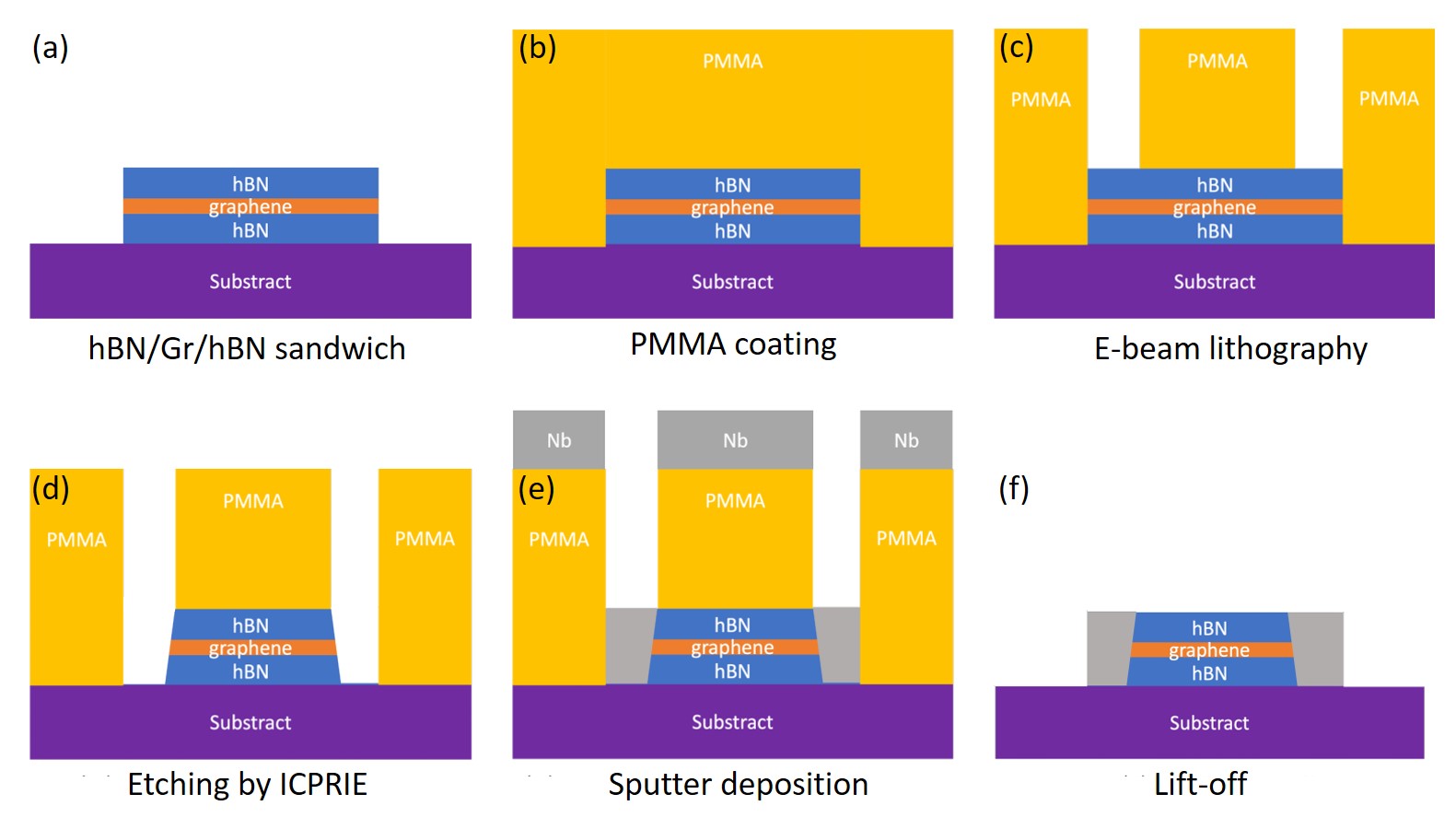
The schematic diagrams for our device fabrication processes are illustrated in Fig. S1. We first prepare the hBN/graphene/hBN sandwich on intrinsic Si wafers capped with 90 nm SiO2 (substrate) using the polymer-free dry transfer method R. et al. (2010); Mayorov et al. (2011); Haigh et al. (2012); Wang et al. (2013). Fig. S2 (a) shows the optical micrograph of the as-transferred heterostructure (device 1), with a graphene flake encapsulated between two hBN layers. After spin coating of PMMA (A6, 500 rpm for 5 s then 4000 rpm for 55 s, bake at 170 ∘C for 2 mins), electron beam lithography (EBL) was used to define the pattern for capacitor pads and SQUID contacts. After EBL exposure and developing, the optical micrograph of device 1 at this stage is shown in Fig. S2 (b). In our SQUIDs, we have designed three contacts across the graphene layer, with a contact width of 2 m and a 500 nm gap between each other. The extension of SQUID contacts connects to a pair of capacitor pads, each with a dimension of 600 m 320 m. In order to make edge contact to the encapsulated graphene, a Inductively Coupled Plasma Reactive-Ion Etching (ICP-RIE) technique was performed, using CHF3 and O2 gases with a ratio of 20:1 (power: 150 W and bias: 20 V), to selectively remove the hBN and graphene layers. This allows us to create the desired side contact geometry. Subsequently, 120 nm niobium (Nb) was sputtered (pressure: 3 mTorr, power: 25 W and sputtering rate: 6 nm/min) right after the etching process, ensuring minimal contact resistance. After lift-off, the optical micrograph of as-fabricated device 1 and device 3 are shown in Fig. S2 (c) and (d), respectively. Our 3D cavity transmon-type devices consist of two capacitor pads linking by two JJs. The capacitor pads not only form a shunting capacitor for transmon architecture but also work as an antenna to interact with microwave photons in 3D cavities.
II II. Measurement scheme
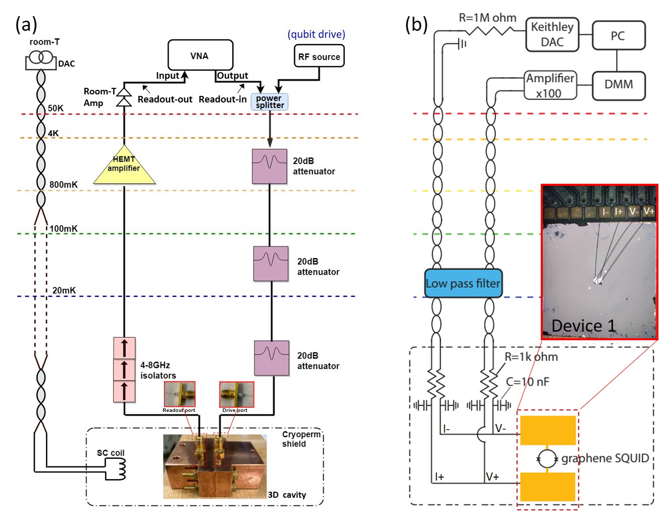
Our 3D cavity transmon-type devices allow both microwave measurements and DC transport measurements. All the experiments detailed in the main text were performed in a dilution refrigerator with a base temperature of 10 mK. In this section, we will introduce the measurement scheme for both microwave [Fig. S3 (a)] and transport measurements [Fig. S3 (b)].
3D cavities need to be carefully calibrated before accommodating devices for microwave measurements. Our 3D copper cavity is milled from two pieces, one half consisting of a pin to drive qubits (drive port), and another with a pin to read qubits (readout port). The insertion depth of the pin within the ports determine pin’s quality factors. Typically the readout port with lower quality factor consists of a longer pin, which has higher visibility to the cavity photons, and thus couples strongly with the EM fields. In contrast, the drive port with higher quality factor consists of a shorter pin, thus limiting the leakage of photons through it. The quality factor of each pin is found by the formula of reflection parameter = , where is the cavity resonance frequency, is the Q value of the tested pin, and is the internal Q value of the 3D cavity Nguyen (2020). We measure of each pin with Vector Network Analyzer (VNA), and use the above formula to fit the amplitude and phase curve to the measured data to obtain and of each pin. By carefully cutting pins and measuring the , we generally reach a desired ratio of drive pin to the readout pin of about 3:1 Nguyen (2020).
The measurement of microwave through the two-ports 3D copper cavity is performed with a transmission setup, in which two sets of coaxial lines are utilized: readout-in line serving as the input line while readout-out line as the output line, as shown in Fig. S3 (a). Readout-in line sends microwave from the output port of VNA (Keysight E5071C) to the drive port of 3D cavity. Subsequently, the transmitted signal from the readout port of 3D cavity travels through the readout-out line, finally reaching the input port of the VNA. By using a power splitter, readout-in line can also receive microwave signals from the RF source (Rohde Schwarz SGS100A) to drive the qubit for two-tone measurements. Since the entry of thermal photons from room temperature sources into the cryogenic environment can critically excite the qubits, the readout-in line is heavily attenuated with three 20 dB attenuators connected at different stages of dilution refrigerator. On the other hand, the readout-out line, which has no attenuation (0 dB), is connected to the High Electron Mobility Transistor (HEMT) amplifier at the 4K stage. The HEMT (LNF-LNC4 8C) has about 40 dB of gain and a noise temperature of 2K. To shield the device from thermal radiation from the HEMT amplifier, a set of three isolators are installed. The readout signal is further amplified by two room-temperature amplifiers (in total 40 dB gain) before going into the input of the VNA. In order to provide the necessary magnetic flux, a home-made superconducting coil is used, which is powered by an external DC source (digital-to-analog converter, DAC). The entire measurement setup is illustrated in Fig. S3 (a).
DC measurement is conducted within a dilution refrigerator operating at a base temperature of 10 mK, as illustrated in Fig. S3 (b). To facilitate precise four-wire measurements, the samples are affixed using four-wire connections, comprising a DC current source, two voltage probes, and a ground. The DC current source is established by combining a Keithley DAC voltage source with a range of 10 V and a room temperature 1 M resistor. This setup allowed to generate a stable current in a range of 10 A. Two voltage probes are positioned on either side of the SQUID device, and the resulting voltage difference was then amplified by a room-temperature voltage amplifier, featuring a fixed gain of 100. Throughout the manuscript, it is important to note that the current range and amplification factor remained consistent for all samples. To minimize the impact of external noise, twisted paired wiring is utilized from room temperature down to the mixing chamber level. To further enhance signal quality, two stages of low-pass RC filters are deployed at room temperature and on the printed circuit board (PCB). Additionally, a filter from QDevil is incorporated at the mixing chamber level within the dilution refrigerator, serving the dual purpose of thermalization and noise reduction. All measurements and data acquisition are orchestrated through a dedicated PC.
III III. SQUID oscillations with Fraunhofer effect
The supercurrent of a single junction considering Fraunhofer effect is described as = Wang (2016). Here, is the critical current of junction at zero magnetic field, is the junction length (parallel to supercurrent transmission direction), is the junction width, is the flux quanta, and = is the effective junction length ( is the London penetration depth). The SQUID oscillation modulated by JJ’s Fraunhofer effect is described in equation 1 in the main text. In equation 1, the ratio between and , meaning the ratio between JJ’s area () and SQUID loop area, determines the frequency ratio between the Fraunhofer oscillation and SQUID oscillation. In Fig. S4 (a) and (b), we plot the function , in which x represent the flux and the factor (denoting the the area ratio between SQUID loop and JJ) sets to 10 and 40, respectively. This is to mimic the data as shown in Fig. 3 (a) and (d), in which 10 and 41 SQUID oscillations reside in a Fraunhofer sub-lobe, respectively. Note that in a real case, the period of SQUID oscillation is fixed (as the designed SQUID loop area for three devices are the same) while the period of JJ’s Fraunhofer oscillation varies due to the variation of JJ’s area (i.e., width of graphene flake) from device to device. Here, we fix the period of JJ’s Fraunhofer oscillation while changing that of SQUID oscillation just for easy comparison of the ratio between two periods.
For an asymmetric SQUID with Fraunhofer pattern modulated by two different size junctions (the case of device 1), we construct the function as , in which the first term accounts for the Fraunhofer modulation from the smaller junction JJ1, the second term accounts for that from the larger junction JJ2, and the third term represents the SQUID oscillations. Note that here the function form of SQUID oscillation is still based on a symmetric SQUID, but it does not affect our analysis below as we mainly aim to discuss the interplay between two Fraunhofer patterns. The ratio between the factors 1:4:40 denotes the area ratio between JJ1, JJ2 and SQUID loop, which is based on our analysis ( : = 1:4 for device 1) in section V of SM. The function is plotted in Fig. S4 (c), with red curve indicating the total function value and blue (green) curve indicating the Fraunhofer pattern of JJ1 (JJ2). As can be seen, the SQUID oscillations modulated by a short-period Fraunhofer pattern from JJ2 are further modulated by a long-period Fraunhofer pattern from JJ1. In our microwave measurements as shown in Fig. 3 (a), we observe the Fraunhofer modulation of JJ2 whose sub-lobes contain 10 SQUID oscillations. However, we did not observe the full behavior as shown in Fig. S4 (c) in our transport data shown in Fig. 3 (d). We attribute this to the possible offset between the two Fraunhofer patterns induced by JJ1 and JJ2. As an example, if JJ2’s Fraunhofer central lobe is shifted to JJ1’s Fraunhofer sub-lobe regions, meaning JJ2’s Fraunhofer sub-lobes now locate in JJ1’s Fraunhofer central lobe, one can imagine the SQUID oscillations residing in JJ1’s Fraunhofer central lobe will not be much modulated by JJ2’s sub-lobes, as the the sub-lobe modulation is much weaker. We found relevant clues in the third cool down of device 1, in which we have performed the transport measurements again, as shown in Fig. S5. In Fig. S5 (a), the main features of Fraunhofer pattern remain almost the same as compared to Fig. 3 (d), with now 73 SQUID oscillations residing in the central lobe instead of 82 observed in the second cool down. However, this time we push the magnetic field range far away from the central lobe region, as shown in Fig. S5 (b). As can been seen, there is an new period of Fraunhofer lobe which contains only 22 SQUID oscillations, which is clearly not close to half of 73 and cannot be explained if considering a symmetric SQUID. Thus, this serves as an indication of the existence of another JJ with larger area compared to the one that induces 73 SQUID oscillations in the Fraunhofer central lobe.
In Fig. 4(b), we show the schematically simulated dispersive shift under the influence of Fraunhofer effect based on . We aim to understand how Fraunhofer pattern modify the periodically flux-modulated cavity frequency in SQUID-based transmons. To this purpose and for simplicity, we have set = 1 and = 0 as a reference point. We do this because the qubit punch-out measurements (top panels in Fig. 5) have indicated at zero flux is higher than in all devices. Also, in the flux region where , a Rabi splitting will form and is no longer valid. In Fig. S7, we have shown oscillation with regard to cavity frequency for all devices. We are only interested in Fraunhofer modulation on the maximal , which is well above . Therefore, we set = 0 as a reference and are only interested in the regime where in Fig. 4(b), by ignoring the function values at peculiar points where 0 that result in divergence in function values. We understand that the symmetry of SQUID for device 1-3 are different, which results in different critical current minimum hence determines whether intersects with cavity frequency or not (see Fig. S7). However, since we are only interested in the Fraunhofer modulation on the maximal , the results we got from Fig. 4(b) still hold regardless of SQUID symmetry.
The SQUID oscillation periods obtained from the bottom panels of Fig. 5 are 4.4 T for device 1, 4.07 T for device 2, and 4.728 T for device 3, respectively. There exists a small deviation from the ideal period 8 T estimated from the designed SQUID loop area (16 m 16 m), possibly due the fabrication error or different effective JJ areas in each device. We also note that the Fraunhofer patterns in the transport data exhibit small sample-dependent variations [Fig. 3(d), (e) and (f)], indicating the different uniformity of spuercurrent in the junctions from device to device.
IV IV. coupling strength g estimation
By using Ansys Maxwell 3D software, we simulated the intrinsic capacitance between the capacitor pads along with non-connected SQUID contacts, including the effects of the cavity. By applying the voltage of 1V for one pad while keeping the other pad at 0 V, the capacitance between the pads is determined to be 92 fF. Based on the dispersive shift obtained from the qubit punch-out measurements, along with the SQUID critical current obtained from DC transport, we can estimate the qubit-cavity coupling strength using and . Since qubit frequency , we need to know both charging energy = and Josephson energy = . We can first obtain 210.5 MHz, using capacitance = 92 fF obtained form our simulation. Next, we need to know SQUID critical current to estimate . Note that from our discussions in the main text, we speculate there exists a remanent magnetic field in our superconducting coil, so we have to choose the critical current residing in the Fraunhofer sub-lobe (i.e., outside central lobe region) in the transport data. Therefore, 0.2 A for device 1 [Fig. 3(d)], 0.1 A for device 2 [Fig. 3(e)] and 0.2 A for device 3 [Fig. 3(f)]. Hence, 99.337 GHz for device 1, 49.668 GHz for device 2 and 99.337 GHz for device 3. Combined all the parameters, we can estimate qubit frequency 12.935 GHz and = 12.935 GHz - 5.4955 GHz 7.44 GHz for device 1, 9.146 GHz and = 9.146 GHz 5.5135 GHz 3.63 GHz for device 2 and 12.935 GHz and = 12.935 GHz 6.034 GHz 6.9 GHz for device 3. Making 13.67 MHz = , = 318.9 MHz can be inferred for device 1; 0.48 MHz = , = 41.76 MHz can be inferred for device 2; 0.68 MHz = , = 68.5 MHz can be inferred for device 3. Note that all three devices have the same capacitor design and almost identical SQUID contact geometry. We attribute the variation of in different devices to the different distribution of graphite flake remaining after the transfer process. We have tested the transmission (S21) of the same cavity loaded with different devices (in similar designs) at room temperature, and found the total Q can vary from device to device. We suspect the remaining metallic graphite pieces interact with microwave, thus amend the distribution of electromagnetic field inside the cavity, thus causing the variation of the qubit-cavity coupling strength in different devices.
In the next section, we found that the qubit frequency in device 2 and device 3 intersects with the cavity frequency [Fig. S7 (b) and (c)], while a Rabi splitting was not observed in the flux-tuning data as shown in Fig. 3(b) and (c). This indicates that device 2 and device 3 are not in the strong coupling regime: and , where is the cavity decay rate and is the qubit total decay rate Blais et al. (2004). From the qubit punch-out measurements shown in the top panels of Fig. 5(b) and (c), we can estimate 10 MHz for device 2 and 20 MHz for device 3, based on the full width at half maximum (FWHM) of the cavity response at low powers. Thus, in both devices, is large enough compared to (41.76 MHz 10 MHz for device 2 and 68.5 MHz 20 MHz for device 3), while Rabi splitting is still absent. This suggest that is not greater than , from which we can estimate the upper bound of qubit coherence time as discussed in the main text.
V V. SQUID symmetry analysis
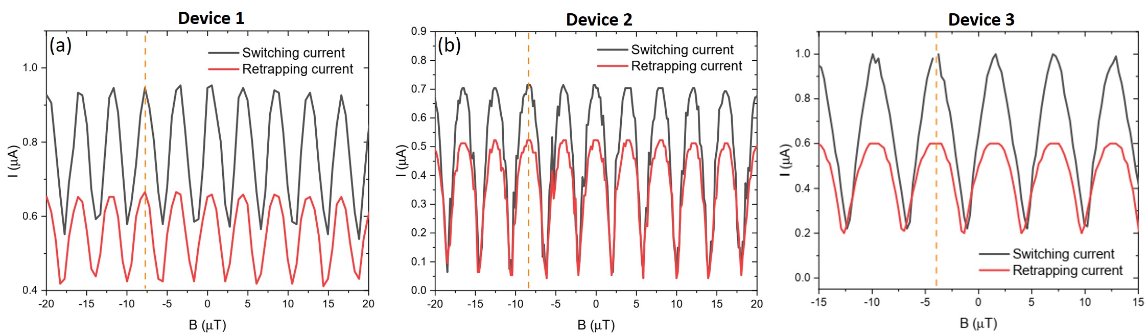
To give a qualitative analysis of the supercurrent in the individual Josephson junction of the SQUID, we plot the switching current and retrapping current as the function of the magnetic field as shown in Fig. S6 for device 1, 2 and 3. Based on the result of the current-to-phase (CPR) relationship in Fig. S6, we suggest that the inductance effect is small enough allowing us to analyze the supercurrent for each JJ. Firstly, the supercurrent shows a symmetric shape with respect to phase (magnetic field) without skewness for all devices (see bottom panels of Fig. 5). The asymmetry of CPR can come from the effect of the screening parameter , which can be written as = , where is the maximum current through SQUID, is the inductance, and is the magnetic flux quanta. With a symmetric CPR (i.e, small ), this suggests that the influence of the inductance in the SQUID is negligible. Secondly, we compare the phase offset between switching and retrapping current, defined as , where and are supercurrents for two Josephson junctions in SQUID. In Fig. S6, we plot the switching and retrapping current for all three devices by flipping the retrapping current to the positive side. From the orange dashed lines, we see almost no phase offset from switching respect with retrapping current in all devices. The small phase difference indicates that they are in either symmetric supercurrent case = or small loop inductance case Nanda et al. (2017). Clearly, for all devices, they are not in the case of = since the critical current does not reach zero (especially for device 1) as shown in the bottom panels of Fig. 5, from which we know is close to zero. Thus, based on the two analyses, we conclude that the inductance is relatively small in our devices. With that, we are able to give a rough estimation of the supercurrent for SQUID’s JJs without complex calculation of the inductance of the SQUID system.
We follow ref. Maier et al. (2015) to analyze the symmetry of SQUID in our devices. We chose the SQUID oscillations around = 0 T as shown in the bottom panels of Fig. 5 for analysis. For two junctions with different critical currents , = 1, 2, the maximal SQUID critical current is while the minimal SQUID critical current is . In device 1, 1 A while 0.6 A, from which we obtain 0.2 A and 0.8 A. Similarly, 0.7 A (1 A) while 0.1 A (0.2 A) for device 2 (3), from which we obtain 0.3 A (0.4 A) and 0.4 A (0.6 A) for device 2 (3). Thus, since , : is 1:4 for device 1, 3:4 for device 2 and 2:3 for device 3, respectively. Using and = Krantz et al. (2020) as depicted in the main text, where = 4 (4/3 and 3/2) and = 3/5 (1/7 and 1/5) for device 1 (2 and 3), we plot as a function of in Fig. S7. Note that we have combined all the parameters () to match = 12.935 GHz, 9.146 GHz and 12.935 GHz for device 1, 2 and 3, as estimated in section IV in SM. We did this as we only care about how SQUID symmetry (the ratio between and ) impact the oscillation depth of qubit frequency. As can be seen in Fig. S7, oscillate weakly between 12.935 GHz and 10.02 GHz without intersecting with cavity frequency at 5.4955 GHz, while and from more symmetric SQUIDs oscillate more strongly and intersect with cavity frequencies at 5.5135 GHz and 6.034 GHz, respectively.