Fermi Velocity Dependent Critical Current in Ballistic Bilayer Graphene Josephson Junctions
Abstract
We perform transport measurements on proximitized, ballistic, bilayer graphene Josephson junctions (BGJJs) in the intermediate-to-long junction regime (). We measure the device’s differential resistance as a function of bias current and gate voltage for a range of different temperatures. The extracted critical current follows an exponential trend with temperature: . Here : an expected trend for intermediate-to-long junctions. From , we determine the Fermi velocity of the bilayer graphene, which is found to increase with gate voltage. Simultaneously, we show the carrier density dependence of , which is attributed to the quadratic dispersion of bilayer graphene. This is in contrast to single layer graphene Josephson junctions, where and the Fermi velocity are independent of the carrier density. The carrier density dependence in BGJJs allows for additional tuning parameters in graphene-based Josephson Junction devices.
Ballistic graphene Josephson junctions (GJJs) have been widely utilized as a platform to study various interesting physics that arise at low temperatures from interactions between superconductors and normal metals [1, 2, 3, 4, 5, 6]. The ballistic superconductor-normal metal-superconductor Josephson junction (SNSJJ) hosts Andreev bound states (ABS) which carry supercurrents across the normal region of the JJ; a disorder-free weak link and high transparency at the SN interface are necessary. Hexagonal Boron-Nitride (hBN) encapsulated graphene as the weak link enables highly transparent contacts at the interface whilst keeping graphene clean throughout the fabrication process [7]. Here, we study proximitized, ballistic, bilayer graphene Josephson junctions (BGJJs). Bilayer graphene devices (in contrast to monolayer) allow extra potential tunability via a non-linear dispersion relation, applied displacement field, or lattice rotation [6].
The critical current () of SNSJJ in the intermediate-to-long regime, where the junction length (L) superconducting coherence length (), scales with temperature (T) as . Here, , an energy scale related to ABS level spacing [8, 9, 10, 11, 12]. Note that in the intermediate regime () is found to be suppressed [4]. A previous study of GJJs found that in this regime, the relation is held more precisely when was taken into account along with L, that is: [8]. Monolayer graphene displays a linear dispersion relation, which results in a constant fermi velocity (). Thus, in ballistic GJJs, remains independent of the carrier density. In comparison, bilayer graphene displays a quadratic dispersion relation at low energies. In BGJJs we studied, a back-gate voltage () controls the carrier density; and dependence on is observed. Using , we extract Fermi velocity in bilayer graphene: it is seen that increases with , and saturates to the constant value, , of the monolayer graphene.
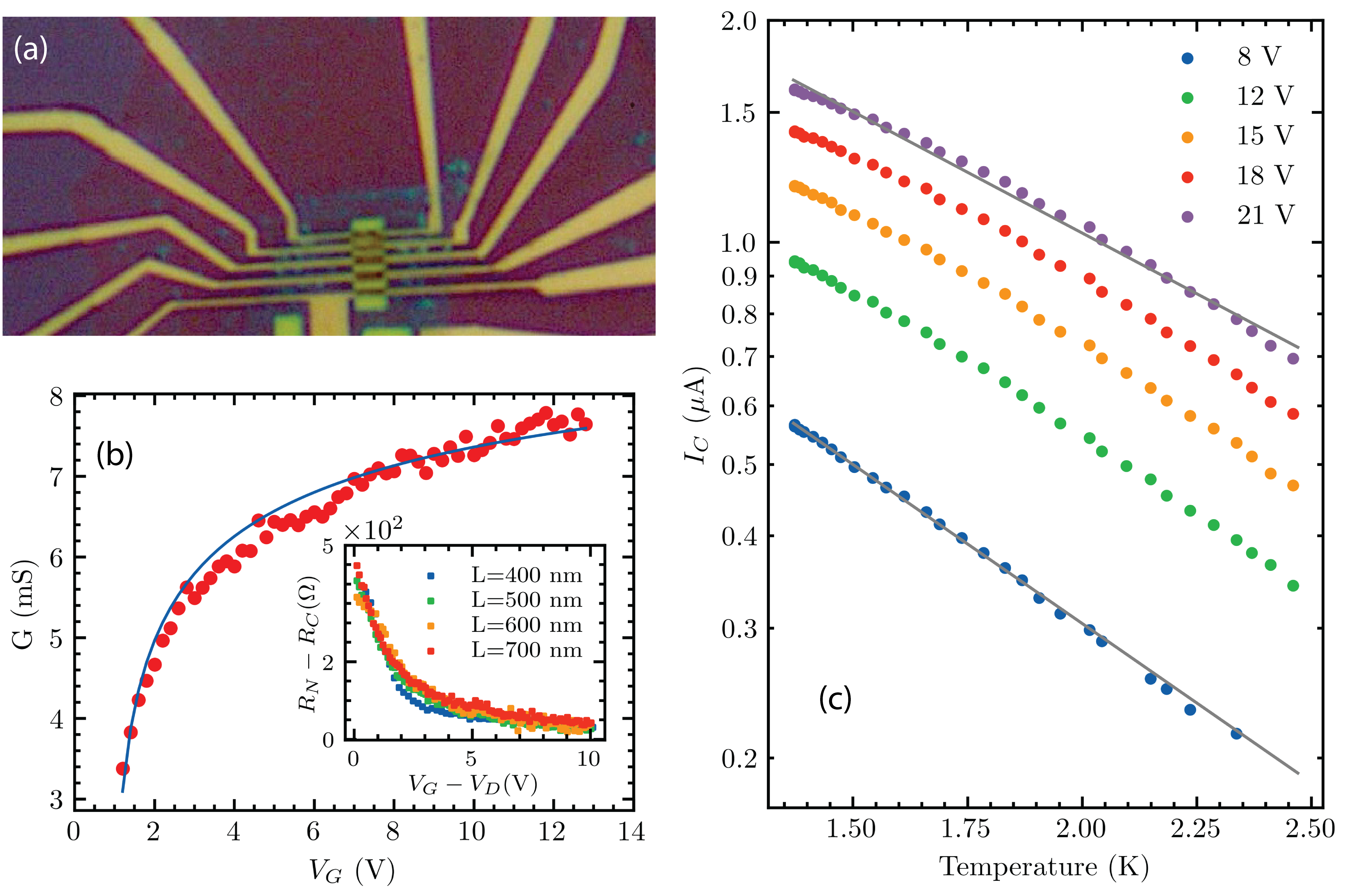
Our device consists of a series of four terminal Josephson junctions (on substrate) made with hBN encapsulated bilayer graphene contacted by Molybdenum-Rhenium (MoRe) electrodes. Bilayer graphene is obtained via the standard exfoliation method. It is then encapsulated in hexagonal Boron-Nitride using the dry transfer method [13]. MoRe of nm thickness is deposited via DC magnetron sputtering. The resulting device has four junctions of lengths nm, nm, nm, and nm. The width of the junctions is m. The device is cooled in a Leiden cryogenics dilution refrigerator operated at temperatures above K, and the measurements were performed using the standard four-probe lock-in method. A gate voltage is applied to the substrate with the oxide layer acting as a dielectric, which allows modulation of the carrier density.[14, 15, 4, 8, 16, 17].
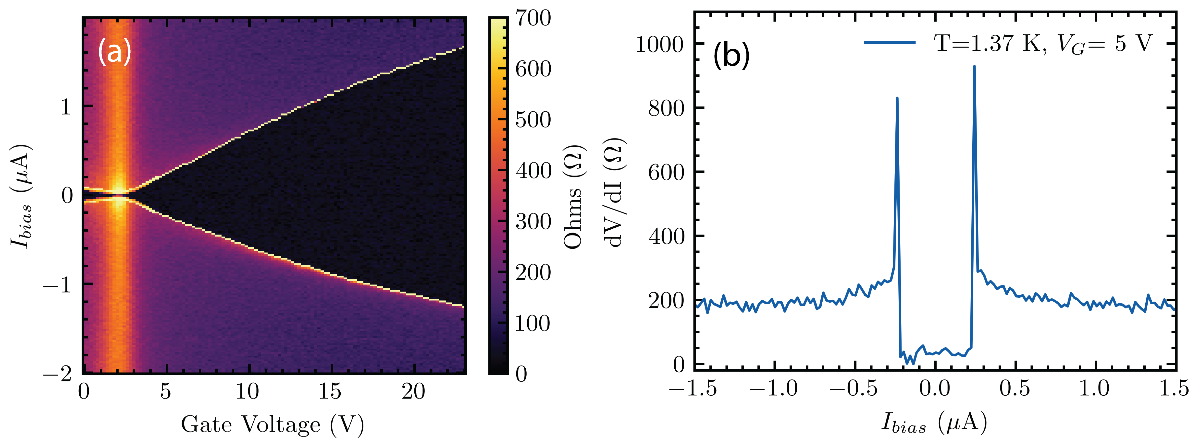
Fig. 1(a) displays the differential resistance () map of the nm junction at K; we see zero resistance (black region) across all applied indicating the presence of supercurrent. As the bias current is swept from negative to positive values, the junction first reaches its superconducting state at a value , known as re-trapping current. Then, as is increased to higher positive values, the junction transitions to the normal state at , known as switching current. Fig. 1(a) shows that the junction can sustain larger region of critical current as we modulate the carrier density to higher values via . Fig. 1(b) displays a line plot extracted from the map which shows hysteresis in and . This is a commonly observed phenomenon in underdamped junctions [18, 14], or can also be attributed self-heating [15, 19, 16]. The critical current of the junction is approximately as found in switching statistics measurements, discussed in previous publications [8, 20, 21, 22].
Extracting the critical current from the differential maps for different temperatures, we can see that falls exponentially with inverse (Fig. 2c) We also extract conductance of the junction in the normal regime (). Fig. 2(b) shows this conductance () for nm junction device. We find that conductance scales as the square-root of as seen from the fit (blue curve). However, due to large contact resistance () of the device, the measured conductance is suppressed compared to the ballistic limit expectation. Therefore, to demonstrate the ballistic nature of the device, we present normal resistances () of junctions of length nm, nm, and nm (Fig. 2(c) inset). Taking into account , we plot extracted values versus from the Dirac point. The inset plot shows that the values are independent of junction length, which demonstrates the ballistic nature of the devices.
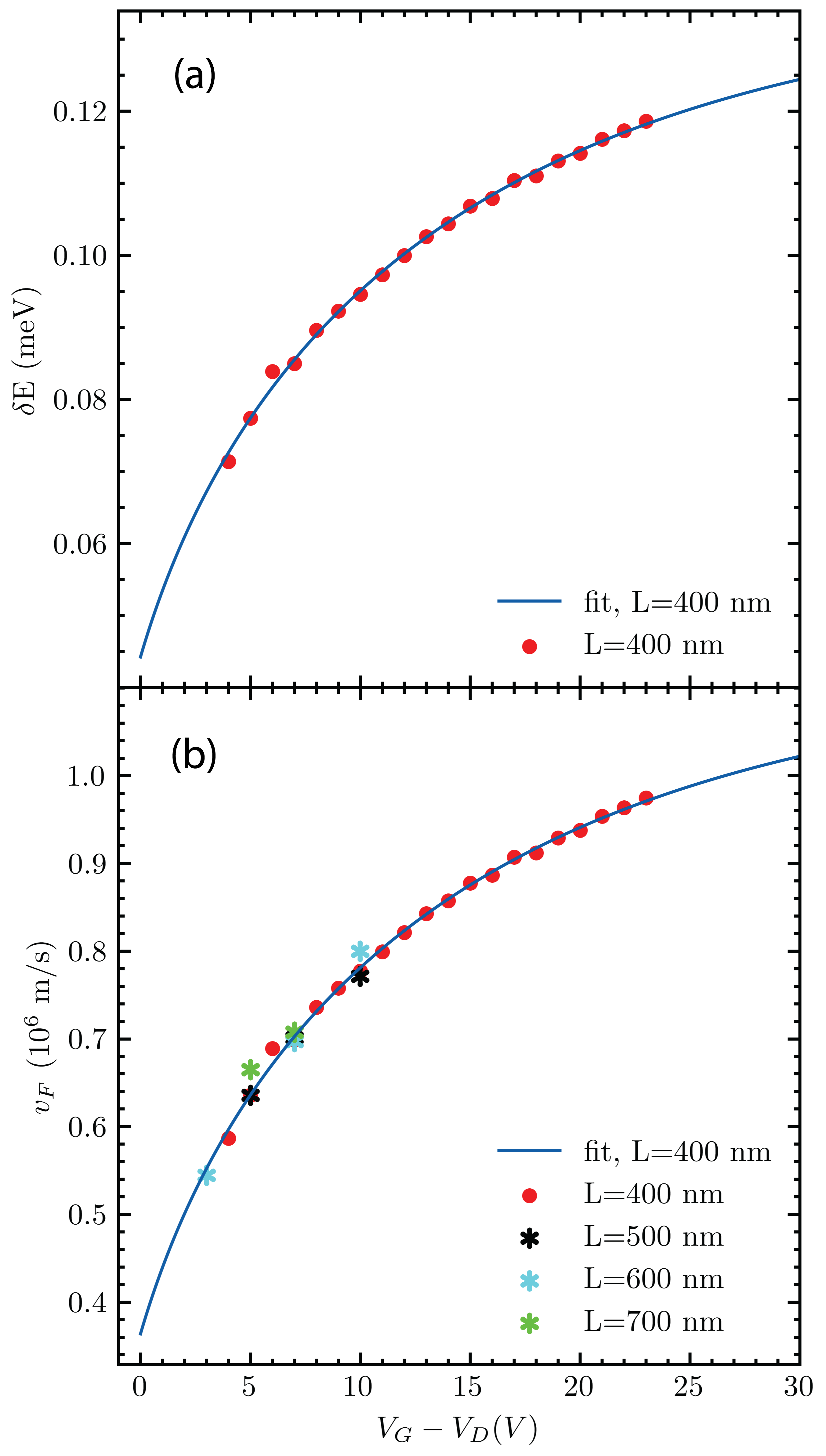
To extract of the junction, we go to the discussion of vs temperature trends in Fig. 2(c). Here the y-axis is plotted in log scale. From the slope of curves for each gate, one can extract versus (plotted in Fig. 3a). Unlike for the case of monolayer graphene, a clear dependence on is seen. The energy scales linearly with Fermi Velocity (Fig. 3b). Note that calculating from for junctions in the intermediate regime requires knowledge of the superconducting coherence length . In our case is obtained from the fit discussed below.
We now compare the experimentally obtained (and ) to the theoretical expectation. Assuming a quadratic dispersion relation , it follows that the expression for the Fermi velocity is: [23, 24, 25]. The Fermi Energy for bilayer graphene scales as: . With being the effective mass of electrons in graphene. The carrier concentration , controlled by the applied gate voltage , is given by with as the gate voltage at the Dirac point. The total capacitance is a combination of quantum capacitance and gate oxide capacitance : . The quantum capacitance for bilayer graphene is determined by . The gate oxide capacitance per unit area is , where is vacuum permittivity, is the relative permittivity of the oxide, and is oxide layer thickness. For Silicon oxide gate with nm we get . Thus, the full expression for the Fermi velocity is:
| (1) |
Note that the effective mass typically ranges from to for carriers/ [26], where is the electron rest mass. Moreover, since has a carrier concentration dependence, we assume a linear shift of with the gate voltage as: [26].
Experimental data provides us with the following: . To fit this data, the model is set as : where are the fitting parameters, and is the independent variable. (We use the as-designed length of the device , and take for .)
The resulting fit of the data from the junction for both and is plotted as solid lines in Fig. 3(a) and Fig. 3(b) respectively. Moreover, taking the fitted , we calculate the Fermi velocity for all other junctions on the same substrate. As seen from Fig. 3(b), the calculated of all devices is in good agreement with the fit obtained from the nm junction. The fitted parameters are summarized in Table 1. All fall within the range of expected values, with being consistent with previously measured values for graphene/MoRe junctions.
| Parameter | Fitted value | Expected Value |
|---|---|---|
| nm | nm | |
| nm | nm | |
| /V | /V | |
| V | V |
In conclusion, we study the evolution of critical current with respect to gate in bilayer graphene Josephson Junctions (BGJJs). Using the critical current-temperature relation expected for intermediate-to-long junctions, we extract the relevant energy scale and find that it has a clear gate dependence. As is proportional to the Fermi velocity in the bilayer graphene, we are able to match the observed gate dependence to the theoretical expectation. Our observation is contrasted with monolayer graphene JJs, that do not have a gate dependent . This result showcases the greater tunability of BGJJs, and offers additional avenues for device characterization.
References
- Chen et al. [2015] W. Chen, D. N. Shi, and D. Y. Xing, Long-range cooper pair splitter with high entanglement production rate, Scientific Reports 5, 10.1038/srep07607 (2015).
- Feigel’man et al. [2008] M. V. Feigel’man, M. A. Skvortsov, and K. S. Tikhonov, Proximity-induced superconductivity in graphene, JETP Letters 88, 747 (2008).
- Shimazaki et al. [2015] Y. Shimazaki, M. Yamamoto, I. V. Borzenets, K. Watanabe, T. Taniguchi, and S. Tarucha, Generation and detection of pure valley current by electrically induced berry curvature in bilayer graphene, Nature Physics 11, 1032–1036 (2015).
- Borzenets et al. [2016a] I. V. Borzenets, Y. Shimazaki, G. F. Jones, M. F. Craciun, S. Russo, M. Yamamoto, and S. Tarucha, High efficiency CVD graphene-lead (pb) cooper pair splitter, Scientific Reports 6, 10.1038/srep23051 (2016a).
- Kroll et al. [2018] J. G. Kroll, W. Uilhoorn, K. L. van der Enden, D. de Jong, K. Watanabe, T. Taniguchi, S. Goswami, M. C. Cassidy, and L. P. Kouwenhoven, Magnetic field compatible circuit quantum electrodynamics with graphene josephson junctions, Nature Communications 9, 10.1038/s41467-018-07124-x (2018).
- Park et al. [2024] G. H. Park, W. Lee, S. Park, K. Watanabe, T. Taniguchi, G. Y. Cho, and G. H. Lee, Controllable andreev bound states in bilayer graphene josephson junctions from short to long junction limits, Physical Review Letters 132, 10.1103/physrevlett.132.226301 (2024).
- Dean et al. [2010] C. R. Dean, A. F. Young, I. Meric, C. Lee, L. Wang, S. Sorgenfrei, K. Watanabe, T. Taniguchi, P. Kim, K. L. Shepard, and J. Hone, Boron nitride substrates for high-quality graphene electronics, Nature Nanotechnology 5, 722 (2010).
- Borzenets et al. [2016b] I. V. Borzenets, F. Amet, C. T. Ke, A. W. Draelos, M. T. Wei, A. Seredinski, K. Watanabe, T. Taniguchi, Y. Bomze, M. Yamamoto, S. Tarucha, and G. Finkelstein, Ballistic graphene josephson junctions from the short to the long junction regimes, Phys. Rev. Lett. 117, 237002 (2016b).
- Kulik [1970] I. O. Kulik, Macroscopic quantization and the proximity effect in s-n-s junctions, Soviet Physics JETP 30, 944 (1970).
- Bardeen and Johnson [1972] J. Bardeen and J. L. Johnson, Josephson current flow in pure superconducting-normal-superconducting junctions, Physical Review B 5, 72–78 (1972).
- Svidzinsky et al. [1972] A. V. Svidzinsky, T. N. Antsygina, and E. N. Bratus, Soviet Physics JETP 3, 860 (1972).
- Svidzinsky et al. [1973] A. V. Svidzinsky, T. N. Antsygina, and E. N. Bratus, Journal of low Temperature Physics 10, 131 (1973).
- Wang et al. [2013] L. Wang, I. Meric, P. Y. Huang, Q. Gao, Y. Gao, H. Tran, T. Taniguchi, K. Watanabe, L. M. Campos, D. A. Muller, J. Guo, P. Kim, J. Hone, K. L. Shepard, and C. R. Dean, One-dimensional electrical contact to a two-dimensional material, Science 342, 614 (2013).
- Borzenets et al. [2011] I. V. Borzenets, U. C. Coskun, S. J. Jones, and G. Finkelstein, Phase diffusion in graphene-based josephson junctions, Physical Review Letters 107, 10.1103/physrevlett.107.137005 (2011).
- Borzenets et al. [2013] I. V. Borzenets, U. C. Coskun, H. T. Mebrahtu, Y. V. Bomze, A. I. Smirnov, and G. Finkelstein, Phonon bottleneck in graphene-based josephson junctions at millikelvin temperatures, Physical Review Letters 111, 10.1103/physrevlett.111.027001 (2013).
- Tang et al. [2022] J. Tang, M. T. Wei, A. Sharma, E. G. Arnault, A. Seredinski, Y. Mehta, K. Watanabe, T. Taniguchi, F. Amet, and I. Borzenets, Overdamped phase diffusion in hbn encapsulated graphene josephson junctions, Phys. Rev. Research 4, 023203 (2022).
- Amet et al. [2016] F. Amet, C. T. Ke, I. V. Borzenets, J. Wang, K. Watanabe, T. Taniguchi, R. S. Deacon, M. Yamamoto, Y. Bomze, S. Tarucha, and G. Finkelstein, Supercurrent in the quantum hall regime, Science 352, 966 (2016).
- Tinkham [2004] M. Tinkham, Introduction to Superconductivity (Dover Publications, 2004).
- Courtois et al. [2008] H. Courtois, M. Meschke, J. T. Peltonen, and J. P. Pekola, Origin of hysteresis in a proximity josephson junction, Physical Review Letters 101, 10.1103/physrevlett.101.067002 (2008).
- Coskun et al. [2012] U. C. Coskun, M. Brenner, T. Hymel, V. Vakaryuk, A. Levchenko, and A. Bezryadin, Distribution of supercurrent switching in graphene under the proximity effect, Physical Review Letters 108, 10.1103/physrevlett.108.097003 (2012).
- Lee et al. [2011] G. H. Lee, D. Jeong, J. H. Choi, Y. J. Doh, and H. J. Lee, Electrically tunable macroscopic quantum tunneling in a graphene-based josephson junction, Physical Review Letters 107, 10.1103/physrevlett.107.146605 (2011).
- Ke et al. [2016] C. T. Ke, I. V. Borzenets, A. W. Draelos, F. Amet, Y. Bomze, G. Jones, M. Craciun, S. Russo, M. Yamamoto, S. Tarucha, and G. Finkelstein, Critical current scaling in long diffusive graphene-based josephson junctions, Nano Letters 16, 4788–4791 (2016).
- Zhu et al. [2009] W. Zhu, V. Perebeinos, M. Freitag, and P. Avouris, Carrier scattering, mobilities, and electrostatic potential in monolayer, bilayer, and trilayer graphene, Physical Review B 80, 10.1103/physrevb.80.235402 (2009).
- Fang et al. [2007] T. Fang, A. Konar, H. Xing, and D. Jena, Carrier statistics and quantum capacitance of graphene sheets and ribbons, Applied Physics Letters 91, 10.1063/1.2776887 (2007).
- Fates et al. [2019] R. Fates, H. Bouridah, and J. P. Raskin, Probing carrier concentration in gated single, bi- and tri-layer cvd graphene using raman spectroscopy, Carbon 149, 390–399 (2019).
- Zou et al. [2011] K. Zou, X. Hong, and J. Zhu, Effective mass of electrons and holes in bilayer graphene: Electron-hole asymmetry and electron-electron interaction, Physical Review B 84, 10.1103/physrevb.84.085408 (2011).