Epitaxial niobium nitride superconducting nanowire single-photon detectors
Abstract
Superconducting nanowires used in single-photon detectors have been realized on amorphous or poly-crystalline films. Here, we report the use of single-crystalline NbN thin films for superconducting nanowire single-photon detectors (SNSPDs). Grown by molecular beam epitaxy (MBE) at high temperature on nearly lattice-matched AlN-on-sapphire substrates, the NbN films exhibit high degree of uniformity and homogeneity. Even with relatively thick films, the fabricated nanowire detectors show saturated internal efficiency at near-IR wavelengths, demonstrating the potential of MBE-grown NbN for realizing large arrays of on-chip SNSPDs and their integration with AlN-based quantum photonic circuits.
Superconducting nanowire single-photon detectors (SNSPDs)1, 2 have become an indispensable resource for a range of quantum and classical applications due to their high detection efficiency over a broad spectrum3, 4, 5, 6, ultra-fast speed7, 8, exceptional timing performance9, 10, 11, and ultra-low dark count noise12, 13. Two categories of superconducting materials have so far been used for the fabrication of high-efficiency SNSPDs – poly-crystalline nitride, and amorphous alloy superconductors. SNSPDs patterned with thin-film amorphous superconducting materials, such as WSi3, 14 and MoSi15, 16, 17, have exhibited excellent homogeneity over a large device area18, 19, 20 due to the absence of grain boundaries. However, they require relatively lower operation temperature and have lower maximum counting rates, resulting from longer hot spot relaxation time in comparison with the SNSPDs made from nitride superconductors, such as NbN21, 22, 23, 24 and NbTiN25, 26, 27, 28, 29. On the other hand, Nb(Ti)N-based detectors have shown relatively superior timing performance, demonstrating <3 ps jitter measured with a short straight nanowire10 and <8 ps with a large-area meandered nanowires30. Despite these advantages, the homogeneity of Nb(Ti)N-SNSPDs are ultimately limited by the poly-crystalline nature of the sputtered Nb(Ti)N films, which could lead to non-uniform distribution of critical currents in a large array of single-photon detectors required for future integrated quantum photonic circuits.
In this Letter, we demonstrate SNSPDs made from single-crystal NbN thin films grown by molecular beam epitaxy (MBE)31 on nearly lattice-matched AlN-on-sapphire substrates. This substrate platform is attractive for the integration of SNSPDs with several other elements of nitride-based photonic integrated circuits 32, 33, 34, 35, 36. The epitaxial NbN films exhibit a high degree of thickness uniformity and structural perfection owing to the 2D layer-by-layer growth unique to MBE technique. The fabricated device consisting of 20 nm-wide and 7 nm-thick nanowire shows saturated internal efficiency at the wavelength of 780 nm and 1050 nm, while further reduction in achievable thin film thickness holds promise for saturating the efficiency at longer wavelength with more relaxed wire width. We expect MBE-NbN on AlN-on-sapphire substrate shown here could provide a scalable material platform for realizing large array of on-chip SNSPDs and integration with nitride-based photonic circuits.
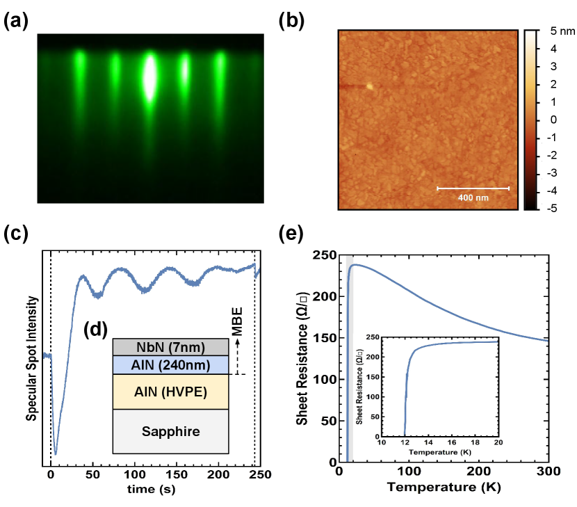
As illustrated in Fig. 1, epitaxial NbN films are grown by radio-frequency plasma-assisted MBE on a commercial 2 inch-diameter c-plane sapphire substrate with a 3 m-thick AlN film grown by hydride vapor phase epitaxy (HVPE). A 240 nm-thick AlN film of Al-polar orientation is grown by MBE, followed by the growth of NbN as shown in Fig. 1(d). During the growth of the films, the reactive nitrogen is generated using a radio-frequency plasma source fed by ultrahigh-purity N2 gas, which is further purified by an in-line purifier. Aluminum (99.9999 purity) is supplied using a Knudsen effusion cell. The Nb flux is generated using an in situ electron-beam evaporator source with 3N5-pure (excluding tantalum, Ta) Nb pellets in a tungsten hearth liner. The NbN films are grown at the temperature of 1100 °C measured by a thermo-couple behind the substrate, at a growth rate of approximately 1.0 nm/min.
The MBE film growth is monitored in situ using a reflection high-energy electron diffraction (RHEED) system operated at 15 kV voltage and 1.5 A current. Figure 1(a) shows sharp and streaky patterns formed by electron diffraction from the smooth surface of the NbN film, indicating the epitaxial nature of the single-crystal NbN film. As shown in Fig. 1(c), the in situ observation of oscillations of the RHEED intensity versus the growth time confirms that the NbN grows in a 2D layer-by-layer growth mode on the AlN surface. The thickness of the NbN film is 7.0 nm, measured by X-ray reflectivity (XRR) with a Rigaku SmartLab diffractometer using CuK1 radiation. Figure 1(b) shows the morphology of the NbN film surface characterized employing tapping mode atomic force microscopy (AFM); the root-mean-square roughness () of the film surface is less than 0.3 nm within a scan size of 1 m1m. In addition, the crystal orientation of the NbN is determined using RHEED and X-ray diffraction (XRD), which indicates the cubic NbN grows with the 1 1 1 crystal axis aligned to the c-axis of AlN.
Figure 1(e) shows the temperature dependence of the sheet resistance of the MBE-NbN thin film with the inset showing a zoom-in view of the superconducting transition region. The transition temperature of the film is measured to be 12.1 K, defined as the temperature where the resistance of the film drops to 50% of the normal-state resistance measured at 20 K. This value is among one of the highest results reported so far for NbN thin films of a few nanometer thickness. The high value is also consistent with the significantly low resistivity of the film, which is calculated to be only 100 obtained by multiplying the thickness with the room-temperature sheet resistance.
We fabricate SNSPD devices by patterning the 7 nm-thick MBE-NbN film. The nanowires are defined by the exposure of negative-tone 6% hydrogen silsesquioxane (HSQ) resist using electron-beam lithography (Raith EBPG 5200) and the subsequent development in 25% tetramethylammonium hydroxide (TMAH) for 2 minutes at room temperature. The HSQ resist is spun at the speed of 4000 rpm, resulting in an approximate thickness of 90 nm. In a second electron-beam lithography step, contact electrodes are defined using double-layer polymethyl methacrylate (PMMA) positive-tone resist. After the development in the mixture of methyl isobutyl ketone (MIBK) and isopropyl alcohol (IPA), we liftoff electron-beam evaporated 10 nm-thick Cr adhesion layer and 100 nm-thick Au in acetone overnight to form the contact pads. The HSQ nanowire pattern is then transferred to the NbN layer in a timed reactive-ion etching (RIE) step employing CF4 chemistry and 50 W RF power. The HSQ resist is left on top of the NbN nanowires after fabrication, serving as a barrier to oxidation.
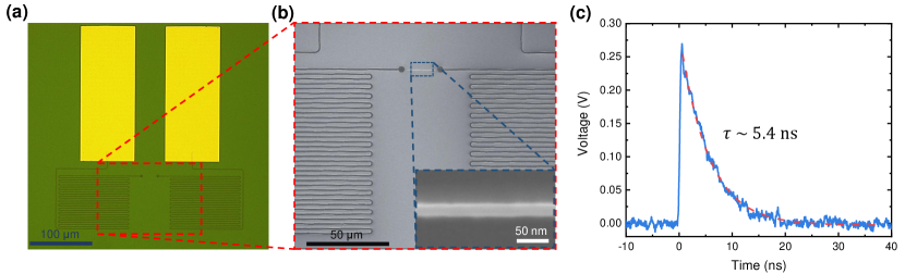
For initial tests, we fabricate short-nanowire detectors with widths ranging from 20 nm to 100 nm for comparison of the internal efficiencies. As shown in Fig. 2(a) and (b), the active detection parts of the devices are made of 20 m-long straight nanowires which are suitable for future waveguide integration. All the nanowires are serially connected to long 1 m-wide meandered wires to prevent the detector latching at high bias currents. The sheet resistance of the devices are measured to be around 180 /sq, which slightly increase compared to the value measured on the bare film prior to fabrication.
In order to characterize the optical response of the fabricated detectors, the detector chip containing multiple devices is mounted on a 3-axis stack of Attocube stages inside a closed-cycle refrigerator and cooled down to 1.7 K base temperature. Continuous wave (CW) laser light with varied wavelength is attenuated to the single-photon level and sent to the detector chip via a standard telecommunication fiber (SMF-28) installed in the refrigerator. The detectors are flood-illuminated by fixing the fiber tip far away from the surface of the detector chip. We control the Attocube stages to move the detector chip at low temperature and make the electrical contact between the RF probes and the gold pads of the detectors. The RF probes are connected to a semi-rigid coaxial cable installed in the refrigerator, while the room-temperature end of the cable is attached to a bias-tee (Mini-Circuits ZFBT-6GW+) to separate the DC bias current and RF output pulses for the detectors. The bias current is supplied by a programmable sourcemeter (Keithley 2401) in conjunction with a low-pass filter (1 kHz cut-off frequency). The output pulses of the detectors are amplified by a low-noise RF amplifier (RF bay LNA-650) and sent to a 4 GHz oscilloscope for the pulse observation or a pulse counter (PicoQuant PicoHarp 300) for the photon counting measurement. Figure 2(c) shows a single-shot trace measurement of the output voltage pulse from the 20 nm-wide detector. The decay time constant extracted from the exponential fitting (red dashed line) is 5.4 ns, which translates into 24 pH/sq sheet kinetic inductance of the NbN film, assuming 50 input impedance of the readout amplifier.
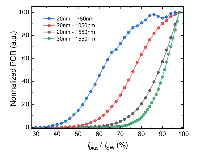
Figure 3 demonstrates the normalized photon counting rates (PCR) as a function of the relative bias current to the switching current () for 20 nm-wide and 30 nm-wide nanowire detectors. of the devices are measured to be 25.5 A and 38.8 A, respectively. As expected, detectors made of narrower nanowires with reduced show better saturated internal efficiencies at shorter wavelength. For 20 nm-wide nanowire detector, we observe a broad saturation plateau at 780 nm wavelength, while the efficiency is only nearly saturated at 1050 nm wavelength. The minor fluctuation in the curve corresponding to 780 nm wavelength is due to the polarization instability of the laser, since the photon absorption of the nanowire is significantly dependent on the polarization status of the incident photons. Neither the 20 nm-wide nor the 30 nm-wide nanowires show saturation behavior at 1550 nm wavelength. We attribute the inefficiency of the detectors to the significantly low electrical resistivity of the MBE-NbN material. In comparison with the SNSPDs made from sputtered21 or atomic-layer-deposited (ALD)24, 37 NbN film of comparable thickness, the nanowires shown in this work demonstrate approximately 3 times reduced sheet resistance as well as sheet kinetic inductance, and in the meantime, 3-5 times improved critical current density. All of these results are in agreement with the 2-3 times lower resistivity of MBE-NbN compared to sputtered or ALD-NbN. Thus, we expect that by further reducing the MBE NbN film thickness down to 2-3 nm, saturated efficiency can be obtained in longer wavelengths with relaxed nanowire widths up to 100 nm. The growth of high crystalline quality NbN films of 3 nm thick or less are achievable by MBE, although a method to protect such thin films from oxidation upon exposure to the ambient is necessary and under investigation. Future work will explore the suitability of such ultra-thin films for SNSPDs.
In summary, we have demonstrated the first SNSPDs patterned from MBE-grown single-crystal NbN thin films on AlN. The 20 nm-wide SNSPDs show saturated internal efficiency at the wavelength of 780 nm and 1050 nm. It is worth mentioning that the AlN-on-sapphire substrate, which the epitaxial growth of NbN relies on, is particularly attractive due to its potential of the on-chip integration of SNSPDs with versatile AlN nanophotonic circuits. The excellent optical functionalities of AlN, such as strong / nonlinearity38 and large electro-optic effect39, 40, renders NbN on AlN-on-sapphire a very attractive material platform for realizing fully integrated quantum photonic circuits with the generation, routing, active manipulation and the final detection of single photons on a single chip.
Acknowledgments
This project is funded by Office of Naval Research grants (N00014-20-1-2126 and N00014-20-1-2176) monitored by Dr. Paul Maki. D.J. acknowledges funding support from NSF RAISE TAQs Award No. 1839196 monitored by Dr. D. Dagenais. H.X.T. acknowledges funding support from DARPA DETECT program through an ARO grant (No: W911NF-16-2-0151), NSF EFRI grant (EFMA-1640959) and the Packard Foundation. The authors would like to thank Sean Rinehart, Kelly Woods, Dr. Yong Sun, and Dr. Michael Rooks at Yale University for their assistance provided in the device fabrication, and Dr. Scott Katzer and Dr. David Meyer at the Naval Research Laboratory for useful discussions. The epitaxial growth was performed at Cornell University, and material characterization used resources made available by the NSF CCMR MRSEC Award No. 1719875. The fabrication of the devices was done at the Yale School of Engineering & Applied Science (SEAS) Cleanroom and the Yale Institute for Nanoscience and Quantum Engineering (YINQE).
References
- Gol’Tsman et al. 2001 G. Gol’Tsman, O. Okunev, G. Chulkova, A. Lipatov, A. Semenov, K. Smirnov, B. Voronov, A. Dzardanov, C. Williams, and R. Sobolewski, “Picosecond superconducting single-photon optical detector,” Applied Physics Letters 79, 705 (2001).
- Hadfield 2009 R. H. Hadfield, “Single-photon detectors for optical quantum information applications,” Nature Photonics 3, 696 (2009).
- Marsili et al. 2013 F. Marsili, V. B. Verma, J. A. Stern, S. Harrington, A. E. Lita, T. Gerrits, I. Vayshenker, B. Baek, M. D. Shaw, R. P. Mirin, and S. W. Nam, “Detecting single infrared photons with 93% system efficiency,” Nature Photonics 7, 210 (2013).
- Verma et al. 2019 V. Verma, A. Lita, B. Korzh, E. Wollman, M. Shaw, R. Mirin, and S. Nam, “Towards single-photon spectroscopy in the mid-infrared using superconducting nanowire single-photon detectors,” in Advanced Photon Counting Techniques XIII, Vol. 10978 (International Society for Optics and Photonics, 2019) p. 109780N.
- Marsili et al. 2012 F. Marsili, F. Bellei, F. Najafi, A. Dane, E. Dauler, R. J. Molnar, and K. K. Berggren, “Efficient single photon detection from 500 nm to 5 m wavelength,” Nano Letters 12, 4799 (2012).
- Reddy et al. 2019 D. V. Reddy, A. E. Lita, S. W. Nam, R. P. Mirin, and V. B. Verma, “Achieving 98% system efficiency at 1550 nm in superconducting nanowire single photon detectors,” in Rochester Conference on Coherence and Quantum Optics (CQO-11) (OSA, 2019).
- Münzberg et al. 2018 J. Münzberg, A. Vetter, F. Beutel, W. Hartmann, S. Ferrari, W. H. Pernice, and C. Rockstuhl, “Superconducting nanowire single-photon detector implemented in a 2d photonic crystal cavity,” Optica 5, 658 (2018).
- Zhang et al. 2019 W. Zhang, J. Huang, C. Zhang, L. You, C. Lv, L. Zhang, H. Li, Z. Wang, and X. Xie, “A 16-pixel interleaved superconducting nanowire single-photon detector array with a maximum count rate exceeding 1.5 GHz,” IEEE Transactions on Applied Superconductivity 29, 1 (2019).
- Zadeh et al. 2018 I. E. Zadeh, J. W. Los, R. Gourgues, G. Bulgarini, S. M. Dobrovolskiy, V. Zwiller, and S. N. Dorenbos, “A single-photon detector with high efficiency and sub-10ps time resolution,” arXiv preprint arXiv:1801.06574 (2018).
- Korzh et al. 2020 B. Korzh, Q.-Y. Zhao, J. P. Allmaras, S. Frasca, T. M. Autry, E. A. Bersin, A. D. Beyer, R. M. Briggs, B. Bumble, M. Colangelo, G. M. Crouch, A. E. Dane, T. Gerrits, A. E. Lita, F. Marsili, G. Moody, C. Peña, E. Ramirez, J. D. Rezac, N. Sinclair, M. J. Stevens, A. E. Velasco, V. B. Verma, E. E. Wollman, S. Xie, D. Zhu, P. D. Hale, M. Spiropulu, K. L. Silverman, R. P. Mirin, S. W. Nam, A. G. Kozorezov, M. D. Shaw, and K. K. Berggren, “Demonstration of sub-3 ps temporal resolution with a superconducting nanowire single-photon detector,” Nature Photonics (2020).
- Zadeh et al. 2020a I. E. Zadeh, J. W. Los, R. Gourgues, J. Chang, A. W. Elshaari, J. Zichi, Y. J. van Staaden, J. Swens, N. Kalhor, A. Guardiani, et al., “A platform for high performance photon correlation measurements,” arXiv preprint arXiv:2003.09916 (2020a).
- Schuck et al. 2013 C. Schuck, W. H. P. Pernice, and H. X. Tang, “Waveguide integrated low noise NbTiN nanowire single-photon detectors with milli-Hz dark count rate,” Scientific Reports 3, 1893 (2013).
- Shibata et al. 2015 H. Shibata, K. Shimizu, H. Takesue, and Y. Tokura, “Ultimate low system dark-count rate for superconducting nanowire single-photon detector,” Optics Letters 40, 3428 (2015).
- Baek et al. 2011 B. Baek, A. E. Lita, V. Verma, and S. W. Nam, “Superconducting a-WxSi1-x nanowire single-photon detector with saturated internal quantum efficiency from visible to 1850 nm,” Applied Physics Letters 98, 251105 (2011).
- Caloz et al. 2018 M. Caloz, M. Perrenoud, C. Autebert, B. Korzh, M. Weiss, C. Schönenberger, R. J. Warburton, H. Zbinden, and F. Bussières, “High-detection efficiency and low-timing jitter with amorphous superconducting nanowire single-photon detectors,” Applied Physics Letters 112, 061103 (2018).
- Korneeva et al. 2014 Y. P. Korneeva, M. Y. Mikhailov, Y. P. Pershin, N. Manova, A. Divochiy, Y. B. Vakhtomin, A. Korneev, K. Smirnov, A. Sivakov, A. Y. Devizenko, et al., “Superconducting single-photon detector made of MoSi film,” Superconductor Science and Technology 27, 095012 (2014).
- Li et al. 2016 J. Li, R. A. Kirkwood, L. J. Baker, D. Bosworth, K. Erotokritou, A. Banerjee, R. M. Heath, C. M. Natarajan, Z. H. Barber, M. Sorel, et al., “Nano-optical single-photon response mapping of waveguide integrated molybdenum silicide (MoSi) superconducting nanowires,” Optics Express 24, 13931 (2016).
- Chiles et al. 2020 J. Chiles, S. M. Buckley, A. Lita, V. B. Verma, J. Allmaras, B. Korzh, M. D. Shaw, J. M. Shainline, R. P. Mirin, and S. W. Nam, “Superconducting microwire detectors with single-photon sensitivity in the near-infrared,” arXiv preprint arXiv:2002.12858 (2020).
- Charaev et al. 2020 I. Charaev, Y. Morimoto, A. Dane, A. Agarwal, M. Colangelo, and K. K. Berggren, “Large-area microwire MoSi single-photon detectors at 1550 nm wavelength,” Applied Physics Letters 116, 242603 (2020).
- Wollman et al. 2019 E. E. Wollman, V. B. Verma, A. E. Lita, W. H. Farr, M. D. Shaw, R. P. Mirin, and S. W. Nam, “Kilopixel array of superconducting nanowire single-photon detectors,” Optics Express 27, 35279 (2019).
- Zhang et al. 2017 W. Zhang, L. You, H. Li, J. Huang, C. Lv, L. Zhang, X. Liu, J. Wu, Z. Wang, and X. Xie, “NbN superconducting nanowire single photon detector with efficiency over 90% at 1550 nm wavelength operational at compact cryocooler temperature,” Science China Physics, Mechanics & Astronomy 60, 120314 (2017).
- Kahl et al. 2015 O. Kahl, S. Ferrari, V. Kovalyuk, G. N. Goltsman, A. Korneev, and W. H. Pernice, “Waveguide integrated superconducting single-photon detectors with high internal quantum efficiency at telecom wavelengths,” Scientific Reports 5, 10941 (2015).
- Pernice et al. 2012 W. Pernice, C. Schuck, O. Minaeva, M. Li, G. Goltsman, A. Sergienko, and H. Tang, “High-speed and high-efficiency travelling wave single-photon detectors embedded in nanophotonic circuits,” Nature Communications 3, 1325 (2012).
- Cheng et al. 2019a R. Cheng, S. Wang, and H. X. Tang, “Superconducting nanowire single-photon detectors fabricated from atomic-layer-deposited NbN,” Applied Physics Letters 115, 241101 (2019a).
- Esmaeil Zadeh et al. 2017 I. Esmaeil Zadeh, J. W. Los, R. B. Gourgues, V. Steinmetz, G. Bulgarini, S. M. Dobrovolskiy, V. Zwiller, and S. N. Dorenbos, “Single-photon detectors combining high efficiency, high detection rates, and ultra-high timing resolution,” APL Photonics 2, 111301 (2017).
- Cheng et al. 2017 R. Cheng, M. Poot, X. Guo, L. Fan, and H. X. Tang, “Large-area superconducting nanowire single-photon detector with double-stage avalanche structure,” IEEE Transactions on Applied Superconductivity 27, 1 (2017).
- Cheng et al. 2016 R. Cheng, X. Guo, X. Ma, L. Fan, K. Y. Fong, M. Poot, and H. X. Tang, “Self-aligned multi-channel superconducting nanowire single-photon detectors,” Optics Express 24, 27070 (2016).
- Miki et al. 2017 S. Miki, M. Yabuno, T. Yamashita, and H. Terai, “Stable, high-performance operation of a fiber-coupled superconducting nanowire avalanche photon detector,” Optics Express 25, 6796 (2017).
- Machhadani et al. 2019 H. Machhadani, J. Zichi, C. Bougerol, S. Lequien, J.-L. Thomassin, N. Mollard, A. Mukhtarova, V. Zwiller, J.-M. Gérard, and E. Monroy, “Improvement of the critical temperature of NbTiN films on III-nitride substrates,” Superconductor Science and Technology 32, 035008 (2019).
- Zadeh et al. 2020b I. E. Zadeh, J. W. N. Los, R. B. M. Gourgues, J. Chang, A. W. Elshaari, J. R. Zichi, Y. J. van Staaden, J. P. E. Swens, N. Kalhor, A. Guardiani, Y. Meng, K. Zou, S. Dobrovolskiy, A. W. Fognini, D. R. Schaart, D. Dalacu, P. J. Poole, M. E. Reimer, X. Hu, S. F. Pereira, V. Zwiller, and S. N. Dorenbos, “Efficient single-photon detection with 7.7 ps time resolution for photon correlation measurements,” ACS Photonics (2020b).
- Yan et al. 2018 R. Yan, G. Khalsa, S. Vishwanath, Y. Han, J. Wright, S. Rouvimov, D. S. Katzer, N. Nepal, B. P. Downey, D. A. Muller, H. G. Xing, D. J. Meyer, and D. Jena, “GaN/NbN epitaxial semiconductor/superconductor heterostructures,” Nature 555, 183 (2018).
- Ferrari et al. 2018 S. Ferrari, C. Schuck, and W. Pernice, “Waveguide-integrated superconducting nanowire single-photon detectors,” Nanophotonics 7 (2018).
- Cheng et al. 2019b R. Cheng, C.-L. Zou, X. Guo, S. Wang, X. Han, and H. X. Tang, “Broadband on-chip single-photon spectrometer,” Nature Communications 10, 1 (2019b).
- Gaggero et al. 2019 A. Gaggero, F. Martini, F. Mattioli, F. Chiarello, R. Cernansky, A. Politi, and R. Leoni, “Amplitude-multiplexed readout of single photon detectors based on superconducting nanowires,” Optica 6, 823 (2019).
- Najafi et al. 2015 F. Najafi, J. Mower, N. C. Harris, F. Bellei, A. Dane, C. Lee, X. Hu, P. Kharel, F. Marsili, S. Assefa, K. K. Berggren, and D. Englund, “On-chip detection of non-classical light by scalable integration of single-photon detectors,” Nature Communications 6, 5873 (2015).
- Cheng et al. 2020 R. Cheng, S. Wang, C.-L. Zou, and H. Tang, “Design of micron-long superconducting nanowire perfect absorber for efficient high speed single-photon detection,” Photonics Research (2020).
- Sayem et al. 2019 A. A. Sayem, R. Cheng, S. Wang, and H. X. Tang, “Lithium-niobate-on-insulator waveguide-integrated superconducting nanowire single-photon detectors,” arXiv preprint arXiv:1912.09418 (2019).
- Guo et al. 2017 X. Guo, C.-L. Zou, C. Schuck, H. Jung, R. Cheng, and H. X. Tang, “Parametric down-conversion photon-pair source on a nanophotonic chip,” Light: Science & Applications 6, e16249 (2017).
- Fan et al. 2018 L. Fan, C.-L. Zou, R. Cheng, X. Guo, X. Han, Z. Gong, S. Wang, and H. X. Tang, “Superconducting cavity electro-optics: A platform for coherent photon conversion between superconducting and photonic circuits,” Science Advances 4, eaar4994 (2018).
- Xiong et al. 2012 C. Xiong, W. H. P. Pernice, X. Sun, C. Schuck, K. Y. Fong, and H. X. Tang, “Aluminum nitride as a new material for chip-scale optomechanics and nonlinear optics,” New Journal of Physics 14, 095014 (2012).