Emerging versatile two-dimensional MoSi2N4 family
Abstract
The discovery of two-dimensional (2D) layered MoSi2N4 and WSi2N4 without knowing their 3D parents by chemical vapor deposition in 2020 has stimulated extensive studies of 2D MA2Z4 system due to its structural complexity and diversity as well as versatile and intriguing properties. Here, a comprehensive overview on the state-of-the-art progress of this 2D MA2Z4 family is presented. Starting by describing the unique sandwich structural characteristics of the emerging monolayer MA2Z4, we summarize and anatomize their versatile properties including mechanics, piezoelectricity, thermal transport, electronics, optics/optoelectronics, and magnetism. The property tunability via strain engineering, surface functionalization and layered strategy is also elaborated. Theoretical and experimental attempts or advances in applying 2D MA2Z4 to transistors, photocatalysts, batteries and gas sensors are then reviewed to show its prospective applications over a vast territory. We further discuss new opportunities and suggest prospects for this emerging 2D family. The overview is anticipated to guide the further understanding and exploration on 2D MA2Z4.
I introduction
Two-dimensional (2D) materials have intrigued great attentions over the years since their fantastic characteristics are close to and even superior than their bulk counterparts, for instance, excellent mechanical properties [1, 2, 3], ultrahigh heat conduction [4, 5, 6], unique quantum effects in low dimensions (e.g., superconductivity and quantum hall effect, etc.) [7, 8, 9, 10, 11]. Since graphene has been successfully prepared by mechanical exfoliation [12, 13, 14], most 2D members have been prepared by the top-down exfoliation of their naturally existed bulk parent materials, e.g., mechanical stripping materials (MoS2, h-BH, NbSe2, MnBi2Te4) [15, 16, 17], interface-assisted exfoliation materials (black phosphorene, FeSe, Fe3GeTe2, RuCl3, PtSe2, PtTe2, PdTe2, and CrSiTe3) [18, 19], and fluid dynamics assisted exfoliation [20, 21, 22]. However, their structures are essentially limited by the parent materials. Bottom-up growth method, an another fabrication strategy, has been applied to synthesize dozens of novel 2D materials, e.g., monolayer borophene by direct evaporation [23, 24], multilayer TMDs by chemical vapor deposition (CVD) [25, 26], 2D van der Waals (vdW) heterostructures designed by mechanically assembled stacks [27], and other materials prepared via layer-by-layer stacking in a specific sequence. However, 2D materials synthesized by this method face the challenge of discontinuous growth due to the surface energy constraints.
Recently, Ren and the coworkers successfully prepared novel 2D layer materials (MoSi2N4 and WSi2N4) without knowing their 3D parents, and broke through the obstacle of island growth [28]. In their growing process, a Cu/Mo bilayer was used as the substrate and NH3 gas as the nitrogen source. The crucial point of layer growth by CVD is that the appropriate atomic passivation of surface dangling bonds favors the decrement of surface energy. The growth diagrams of 2D molybdenum nitride without (MoN2) or with Si (MoSi2N4) are shown in Fig. 1(a). The growing progress of MoN2 without Si shows the obvious island domains and finally uneven micrometer-scale domains (appropriately 10 nm thick) form. On the contrary, MoN2 with Si (MoSi2N4) firstly forms as triangular domains with uniform thickness, then expands to a centimeter-scale uniform polycrystalline film, and eventually maintains great ambient stabilization, as shown in Fig. 1(b). The high-angle annular dark field scanning TEM (HAADF-STEM) observation (Fig. 1(c) and (d)) indicates that MoSi2N4 is a MoN2-derived septuple-atomic-layer compound built up in the order of N-Si-N-Mo-N-Si-N. The vdW form of MoSi2N4 can be grown layer by layer due to the free of dangling bonds, indicating the possibility of large-scale preparation of this 2D compound.

Thanks to the breakthrough achievement in experimental synthesis, series of theoretical studies on MoSi2N4 and its derived materials have been further carried out. Density functional theory (DFT) calculations define this septuple-atomic-layer compounds as 2D MA2Z4 family [29]. This 2D ternary material includes group IVB, VB and VIB elements for M-site atom, group IVA elements for A-site atom and group VA elements for Z-site atom. The general approach to design MA2Z4 family layered van der Waals materials is proposed by intercalating MoS2-type MZ2 layer into an InSe-type A2Z2 monolayer (Fig. 1(e)) [29]. If 2H and 1T phases of MZ2 and and phases of A2Z2 are considered, 4 types of monolayer MA2Z4 nanosheets can be obtained, i.e., -MA2Z4 ( = 1–6), -MA2Z4 ( = 1–12), -MA2Z4 ( = 1–3) and -MA2Z4 ( = 1–9). In total, there exist 30 structures of this family by removing duplicate symmetry and abandoning the structures that are energetically unstable. Five stable structures of 2D MA2Z4 are shown in Fig. 1(f). The experimentally synthesized and the most widely studied structure is -MA2Z4. Due to the rich compositions and diverse structures, MA2Z4 family has exhibited intriguing physical and chemical characteristics, such as non-linear optics and second harmonic response [30, 31], quantum behavior of strong exciton-phonon coupling in -MoSi2N4 [32, 33], spin polarization and plasmon properties in -MoSi2N4 [34, 35], superconductivity in -TaSi2N4 and NbSi2N4 [36], topological insulating property in -SrGa2Se4 and SrGa2Te4 [29], ferromagnetic nature in -VSi2P4 [29], valley-half-semiconducting property in -VSi2N4 [37], Mott transition in XSi2N4 [38], etc. These intriguing properties could enable promising applications of MA2Z4 family in nanoelectronic devices such as magnetic tunnel junction, field effect transistors, highly sensitive and reusable gas sensors, etc. [39, 40, 41, 42, 43, 44, 45, 46]
In this paper, we aim to review the recent progress of the novel 2D layered MA2Z4 family, in terms of its structures, versatile properties and perspective applications. After introducing the diverse structures in Fig. 1, we provide an extensive overview on the versatile properties regarding to mechanics, piezoelectricity, thermal transport, electronics, optics/optoelectronics, and magnetism. The tunability of each property via strain engineering, surface functionalization and layered strategy (e.g., multilayer or heterostructure) is also expounded. Then, we introduce the perspective applications derived from the excellent properties of MA2Z4, including transistors, photocatalysts, batteries and sensors. Finally, we summarize the outstanding advantages of this family and suggest the conceivable outlook in the future.
| Struc. | Phase | |||||||||
|---|---|---|---|---|---|---|---|---|---|---|
| (Å) | (eV) | (eV) | (cm2V-1s-1) | (GPa) | (Wm-1K-1) | |||||
| MoSi2N4 | 2.91 | 1.74(-K) | 2.31(-K) | 200 | 1000 | 491.4139.1 GPa | 65.818.3 | 0.28 | 417–439 | |
| MoSi2P4 | 3.47 | 0.70(K-K) | 0.99(K-K) | 246–258 | 1065–1429 | 159 GPa | 17.5-21.2 | * | 116–122 | |
| 3.46 | 0.91(K-K) | 1.19(K-K) | * | * | * | * | * | * | ||
| MoSi2As4 | 3.62 | 0.56(K-K) | 0.98(K-K) | * | * | * | * | * | 46 | |
| 3.61 | 0.74(K-K) | 1.02(K-K) | * | * | * | * | * | * | ||
| MoGe2N4 | 3.02–3.04 | 0.91–0.99(K-K) | 1.27–1.38(K-K) | 490 | 2190 | 362 GPa | 40.3–42.1 | * | 286 | |
| MoGe2P4 | 3.55 | 0.04(-K) | 0.84(-K) | * | * | 139 GPa | 15.3–18.4 | * | 63 | |
| 3.53 | 0.56(K-K) | 0.95(K-K) | * | * | * | * | * | * | ||
| MoGe2As4 | 3.69 | 0.47(K-K) | 0.83(K-K) | * | * | * | * | * | * | |
| WSi2N4 | 2.91 | 2.08(-K) | 2.57–2.66(-K) | 320 | 2026 | 506 GPa | 55.5–59.2 | 0.27 | 401–503 | |
| WSi2P4 | 3.48 | 0.53(K-K) | 0.81(K-K) | * | * | 167 GPa | 18.8–22.0 | * | 129 | |
| 3.46 | 0.86(K-K) | 1.11(K-K) | * | * | * | * | * | * | ||
| WSi2As4 | 3.61 | 0.71(K-K) | 0.95(K-K) | * | * | * | * | * | * | |
| WGe2N4 | 3.02 | 1.15–1.29(K-K) | 1.51–1.69(K-K) | 690 | 2490 | 384 GPa | 42.6–44.5 | * | 322 | |
| WGe2P4 | 3.55 | 0.48(K-K) | 0.73(K-K) | * | * | 145 GPa | 16.5–19.3 | * | 64 | |
| 3.54 | 0.63(K-K) | 0.89(K-K) | * | * | * | * | * | * | ||
| WGe2As4 | 3.69 | 0.50(K-K) | 0.78(K-K) | * | * | * | * | * | * | |
| CrSi2N4 | 2.84 | 0.49(-K) | 0.94(K-K) | * | * | 468 GPa | 55.4–57.8 | * | 332–348 | |
| CrSi2P4 | 3.42 | 0.28(K-K) | 0.64(K-K) | * | * | 154 GPa | 18.5–21.2 | * | 120 | |
| 3.41 | 0.34(K-K) | 0.65(K-K) | * | * | * | * | * | * | ||
| CrGe2N4 | 2.98 | 0.49(-K) | 0.31(-K) | * | * | 340 GPa | 38.1–38.7 | * | 198 | |
| CrGe2P4 | 3.49 | 0.04(K-K) | 0.36(K-K) | * | * | * | * | * | * | |
| TiSi2N4 | 2.93 | 1.57(M-M) | 2.50(M-M) | * | * | * | * | * | 107 | |
| ZrSi2N4 | 3.04 | 1.55(M-M) | 2.41(M-M) | * | * | 382 N/m | * | 0.32 | 82 | |
| 3.05 | 1.00(-M) | 0.36(-M) | * | * | 400 N/m | * | 0.26 | * | ||
| ZrGe2N4 | 3.19 | 1.04(-) | 2.34(-) | * | * | * | * | * | * | |
| HfSi2N4 | 3.02 | 1.80(M-M) | 2.70(M-M) | * | * | 406 N/m | * | 0.32 | 124 | |
| 3.04 | 1.21(-M) | 2.21(-M) | * | * | 420 N/m | * | 0.25 | * | ||
| HfGe2N4 | 3.18 | 1.15(-) | 2.45(-) | * | * | * | * | * | * | |
| PdSi2N4 | 2.99 | 2.50(-M) | 3.80(-M) | * | * | 356 N/m | * | 0.29 | * | |
| PtSi2N4 | 3.02 | 2.50(-M) | 3.80(-M) | * | * | 349 N/m | * | 0.30 | * | |
II Versatile properties
II.1 Mechanical properties

Since the extraordinary mechanical properties of graphene (103 GPa of the in-plane stiffness and nearly 1 TPa of the elastic modulus [50]), 2D materials with excellent mechanical properties have attracted great attentions. As for MoSi2N4, its experimentally measured tensile strength () and elastic modulus () are 65.818.3 GPa and 491.4139.1 GPa [28], respectively, which are nearly half of those in graphene and higher than those in most 2D TMDs (e.g., 22 GPa and 270100 GPa of MoS2) [3, 51, 52], MXene (e.g., 17 GPa and 333 GPa of Ti3C2Tx [53], 26 GPa and 386 GPa of Nb4C3Tx [54]), and black phosphorene [55] (18 GPa and 166 GPa). In detail, Ren et al. [28] measured the mechanical properties of monolayer MoSi2N4 via atomic force microscopy nanoindentation (Fig. 2(a)). With a diamond tip of 11.1 nm, the indentation of hole is about 23 nm. The elastic behavior of monolayer MoSi2N4 is demonstrated due to the well fitting force-displacement curves of loading and unloading states. Theoretical prediction of mechanical properties of 2D materials is mainly based on the linear elastic model. The theoretically calculated tensile strength and elastic modulus are 48.3–57.8 GPa and 479.1–487.0 GPa, respectively [47, 56, 57], in good agreement with experimental values.

Actually, the critical strain and ideal tensile stress of 2D materials are vital indicators for practical applications, which depend on the elastic limit and lattice vibration [58]. Li et al. [56] focused on the elastic limit and failure mechanism of monolayer MoSi2N4. Under biaxial and uniaxial (zigzag or armchair) strains, the ideal strengths of monolayer MoSi2N4 are similar, about 50 GPa, while the corresponding critical strain is 19.5 (biaxial strain), 26.5 (zigzag strain) and 17.5 (armchair strain). In Fig. 3, when the strains are below 20 ( 20), the tensile stresses () are in the order of . There exists an obvious yield phenomenon under biaxial and armchair strains when 20, but the yield limit under a zigzag strain is about 25. By fitting the initial strain-stress curve based on the linear regression up to 1 strain (the inset of Fig. 3(a)), the elastic moduli are calculated as = 448.3 5.1 GPa and = 457.8 3.9 GPa, which are more than twice those of MoS2 ( = 197.9 4.3 GPa and = 200 3.7 GPa) [59]. The degeneracy of elastic moduli indicate a nearly elastic isotropy in monolayer MoSi2N4. On the other hand, the failure mechanism has been investigated on the aspect of lattice stability by phonon dispersion. When the tensile strength limit is reached under an armchair strain, the phonon dispersion has no imaginary frequency. This indicates lattice stability and further reveals that the failure phenomenon of monolayer MoSi2N4 is ascribed to the elastic failure of the SiN layer before reaching the critical strain. The obvious imaginary frequency of out-of-plane acoustic branch (ZA) before reaching tensile strength limit demonstrates that the failure mechanism of monolayer MoSi2N4 is attributed to phonon instability under the zigzag or biaxial strains.
The mechanical parameters of other members in MA2Z4 family are listed in Table 2. Mortazavi et al. [47] found in MA2Z4 family the mechanical properties are mainly affected by the terminating atom (Z-site) rather than the core atom (M-site). Three possible factors that influence the mechanical properties are proposed: Z-site atomic mass, structure and chemical bonds. Firstly, increasing Z-site atomic weight deteriorates the mechanical properties, but the elastic modulus has little change when M-site atomic mass is increased. For examples, MA2N4 has higher and than MA2P4, while and of MoSi2N4 and WSi2N4 are close. Secondly, since the M-A bonds are absolutely vertical, only M-Z and A-Z bonds participate in the deformation when applying an in-plane loading, indicating that the two bonds related to Z-site atoms determine the mechanical properties. Besides, chemical bonds formed with N atoms are always stronger than those with P/As atoms. Bonds formed with Si are sturdier than those with Ge, resulting in the highest elastic modulus of monolayer MSi2N4.
The mechanical properties of some other MA2Z4-derived materials have also been investigated, e.g., CrC2N4, SnSi2N4, SnGe2N4 and XMoSiN2 (X = S/Se/Te) [60, 61, 62, 63]. The predicted elastic modulus and tensile strength of CrC2N4 are as high as 676 and 54.8 GPa, respectively, while those of SnSi2N4 (478 and 47 GPa) are close to those of MoSi2N4. This indicates that the MA2Z4 structure offers excellent mechanical features, but the intrinsic mechanisms related to the elements and structures require further studies.
II.2 Piezoelectricity, ferroelectricity and flexoelectricity

Piezoelectricity of 2D materials can convert mechanical energy into electrical energy and , which always occurs in semiconductors or insulators with broken inversion symmetry. The relax-ion piezoelectric coefficients ( and ) are expressed as
| (1) |
and
| (2) |
where , , are polarization vector, strain and stress. The subscript or represent the electronic or ionic contributions. The relationship between and is built via elastic tensor (, with the Voigt notation). The independent parameters of tensor are reduced due to the symmetry of crystal structure. In monolayer MA2Z4, the counterpart with space group prohibits the out-of-plane piezoelectric effect, so that only the in-plane piezoelectric strain and stress coefficients (i.e., , ) and elastic coefficients (i.e., , ) are considered [65, 64].
Structure effect on piezoelectricity of MA2Z4 has been investigated [64]. The structures are divided into six configurations by different operations (translation, mirror and rotation) of A2Z2 layers, which are nominated as ( = 1–6), as shown in Fig. 4(a). It is observed that the values of of MSi2N4 (M = Mo, W) are close when = 1, 2, 4, 5, while those of are higher when = 3, 6, indicating and MSi2N4 (M = Mo/W) with high resistance to deformation. The structural sensibility of is homologous with that of from to . of exhibits the largest value among six structures, which is 13.95 C/m for MoSi2N4 and 12.17 C/m for WSi2N4. of -MoSi2N4 and -WSi2N4 is 3.53 and 2.91 pm/V, respectively. of -MoSi2N4 and -WSi2N4 (experimentally synthesized phases) is 1.15 and 0.78 pm/V, respectively.
Studies on the influence of different M/A/Z atoms reveal that of both and improves with the element periodicity increasing (Fig. 4(c)). For instance, of MSi2N4 is in the order of CrSi2N4¡MoSi2N4¡WSi2N4. The larger elastic constants of MA2N4, compared with those of MA2P4 and other 2D materials (e.g., TMDs, metal oxides, and III–V semiconductors [66, 67]), indicate that MA2N4 system is more rigid. The change trend of and follows the opposite regularity, compared with elastic coefficients. of MA2P4 with the same M and A atoms is larger than that of MA2N4 for both and phases. of - and -MA2Z4 is in the range of 0.78–6.12 pm/V and 0.25–5.06 pm/V, respectively. Monolayer MA2P4 nanosheets (e.g., -CrSi2P4, -MoSi2P4, -CrGe2P4, -MoGe2P4 and -CrGe2P4) show excellent piezoelectric response. In addition, the effect of A-site atoms on piezoelectric performance can be ignored so that of MoGe2N4 is close to that of MoSi2N4. of most monolayer MA2P4 nanosheets is even larger than that of 2D TMDs (e.g., = 3.65 pm/V of MoS2, = 2.12 pm/V of WS2, = 4.55 pm/V of MoS2, and = 2.64 pm/V of WSe2) [68] and (3.1 pm/V) of bulk piezoelectric wurtzite GaN [69].
The compressive and tensile biaxial strain are shown to obviously improve and deteriorate the piezoelectric performance of MoSi2N4, respectively (Fig. 4(d)) [65]. Piezoelectric stress and strain responses are improved with the in-plane strain from -4 to 4. can be enhanced by 107 if a rensile biaxial strain of 4 is applied. VSi2P4, a spin-gapless semiconductor (SGS), possesses a wide range of properties due to its strain sensitivity. With the increasing strain, it presents as ferromagnetic metal (FMM), SGS, ferromagnetic semiconductor (FMS), or ferromagnetic half-metal (FMHM) [70]. In the strain range of 1–4, the coexistence of ferromagnetism and piezoelectricity can be achieved in FMS VSi2P4. Its under 1, 2 and 3 strain is 4.61, 4.94 and 5.27 pm/V, respectively.
There exist both in-plane and out-of-plane piezoelectric polarizations in Janus MSiGeN4 (M = Mo/W) owing to the broken reflection symmetry along the out-of-plane direction [71, 72]. The in-plane piezoelectric coefficients of Janus MSiGeN4 ( = 1.494 pm/V for MoSiGeN4, = 1.050 pm/V for WSiGeN4) are between those of MSi2N4 and MGe2N4, while the out-of-plane stress piezoelectric coefficients () are –0.014 and 0.011 pm/V for MoSiGeN4 and WSiGeN4, respectively. Under an in-plane biaxial strain, of MSiGeN4 is improved with the increasing , which is similar with MA2N4. A tensile strain of 10 can increase of MoSiGeN4 and WSiGeN4 by several times, with the values up to 8.081 and 7.282 pm/V, respectively. On the contrary, a compressive biaxial strain can effectively enhance the out-of-plane piezoelectric response. The MA2Z4-derived SrAlGaSe4 has both in-plane ( = –1.865 pm/V/) and out-of-plane ( = –0.068 pm/V) piezoelectricity under uniaxial a tensile strain of 6 [73].
In addition to piezoelectricity, the intrinsic ferroelectricity and its electrical switching in MA2Z4 are still open issues. For example, the sliding ferroelectricity is found in vdW MoA2N4 bilayer and multilayer [74]. The interlayer inequivalence caused by the stacking order directly generates the out-of-plane polarization. Then, the induced vertical polarization can be switched via the interlayer sliding. The calculated vertical polarization is 3.36, 3.05, 2.49 and 3.44 pC/m for AB stacking bilayer MoSi2N4, MoGe2N4, CrSi2N4 and WSi2N4, respectively, which are higher than that of bilayer WTe2 and BN [75, 76].
The flexoelectricity of monolayer MA2Z4 is also of interest, which is often induced by bending deformation of 2D materials with a strain gradient [47]. The out-of-plane bending flexoelectric coefficients of 12 kinds of MA2Z4 (M = Mo/Cr/W, A = Si/Ge, Z = N/P) are found in the range of 0.001–0.047 nC/m under a bending strain gradient of 0.3/Å. The highest flexoelectric coefficient of WGe2N4 is about 1.5 times higher than that of MoS2 [77]. It is proposed that the enhancement of flexoelectricity is insufficient with the bending deformation, but is broadened by the construction of asymmetry structures (e.g., Janus counterparts) [78, 79].
II.3 Thermal conductivity
Owing to the high tensile strength and thus strong bond interactions, the thermal conductivity of monolayer MA2Z4 family has attracted attentions. Based on thermal Boltzmann transport equations, the theoretical lattice thermal conductivity () of MoSi2N4 is predicted as high as 400 Wm-1K-1 at room temperature [47, 49, 80, 81], which is larger than that of most other 2D materials, such as hydrogenated borophene (368 Wm-1K-1) [82], TMDs (23–142 Wm-1K-1) [83, 84, 85], group IVA and VIA compounds (0.26–9.8 Wm-1K-1) [86, 87]. But it is lower than that of graphene (3000–5000 Wm-1K-1) [88, 89], and h-BNs (600 Wm-1K-1) [90]. Such high thermal conductivity of monolayer MoSi2N4 is promising for heat conductors and thermal management in semiconductor devices.

In Slack’s classic rules [91, 92], crystals with high thermal conductivity follows four rules: simple crystal structure, light atomic masses, strong bonding and low anharmonicity. In the monolayer MA2Z4 family, by replacing M/A/Z atoms at different sites, the different contributions to have been further examined [47, 49]. It is found that when Z- site atoms are replaced, of monolayer MA2Z4 obeys the Slack’s rules (red lines in Fig. 5(a)). For instance, of MoSi2Z4 decreases by one order of magnitude from Z = N to As, indicating that Z atom plays a critical role in controlling the thermal conductivity of MoSi2Z4. The similar variation phenomena are found in MoGe2Z4 and WGe2Z4 as well. Meanwhile, in A-site-replaced MA2Z4, is decreased by about 40.3–50.4 from A = Si to Ge. of MoGe2N4 (286 Wm-1K-1) is about 40.3 lower than that of MoSi2N4 (439 Wm-1K-1). of WGe2P4 (64 Wm-1K-1) is only half that of WSi2P4 (129 Wm-1K-1). The decreasing phenomena are intrinsically attributed to the phonon properties. The Z- or A-site atoms of MA2Z4 determine the phonon frequency range. Monolayer MA2N4 shows wider frequency range than MA2P4 and MA2As4 (Fig. 5(b)). MSi2Z4 exhibits wider phonon dispersion than MGe2Z4. Thermal conductivity is related to the phonon group velocity that directly depends on phonon branches. Thus, wider phonon bands lead to higher phonon group velocity and result in higher thermal conduction.
When M atoms are from different group IVB or VIB atoms, the variation of is abnormal and the conventional guideline for searching high does not work. exhibits an irregular oscillation with the increasing atomic mass and decreasing Debye temperature (green dash lines in Fig. 5(a)). Mortazavi et al. proposed that the weight of core atoms is the dominant factor on thermal conduction of MA2Z4 and increases with the weight of core atoms. This violates the Slack’s rules but is consistent with the classical theory that stiffer systems favor a higher . However, in our recent work [49], we found that the influential factors on the variation of is not limited to the atomic mass. For instance, the average mass of WSi2N4 is 1.5 times that of CrSi2N4, but shows only 13 difference. We proposed that the abnormal thermal conductivity of M-site replaced MA2Z4 is relative to the group that M atoms belong to. of MA2Z4 with group VIB M atom is about 3–4 times of that with group IVB M atom. These abnormal phenomena with respect to M atoms are attributed to the fundamental vibrational properties and phonon scattering behavior. The acoustic branches of MA2Z4 with group VIB M are more bunched and less flattened. Consequently, the phonon scattering rates (Fig. 5(c)) of group VIB M-site MA2Z4 are lower than that of group IVB M-site MA2Z4, and higher presents in the former. As shown in Fig. 5(d), the thermal conductivity of monolayer MA2Z4 family is in a very wide range (101–103 Wm-1K-1), locating between that of 2D TMDs and hBN.
II.4 Thermoelectric properties
In addition to the thermal conductivity, the thermoelectric performance of monolayer MA2Z4 has been also investigated. The dimensionless figure of merit () is always used to measure the efficiency of thermoelectric conversion of a thermoelectric material, which is expressed as:
| (3) |
where , , , , and are the Seebeck coefficient, electrical conductivity, working temperature, electronic thermal conductivity and lattice thermal conductivity, respectively. The higher indicates the better heat-to-electricity conversion efficiency. Thus, 2D materials for the thermoelectric field are prone to semiconductors with high Seebeck coefficient, electrical conductivity and low thermal conductivities.
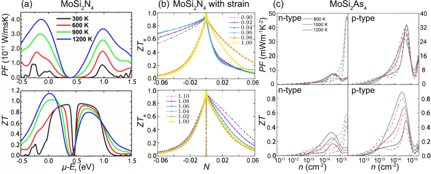
The power factor ( = ) of monolayer MoSi2N4 is studied to evaluate the capability of producing electricity [57]. The heat conversion into electricity is favored by the temperature since increases considerably with temperature. The maximum is located at a chemical potential range of 0.12–0.98 eV (upper in Fig. 6(a)). in the negative chemical potential region is more sensitive to temperature than in the positive region. Meanwhile the maximum increases with temperature in the chemical potential range of -0.45–0.5 eV. The maximum of monolayer MoSi2N4 is up to 1.2 at 1200 K [57], while of MoGe2N4 is up to 1.0 at 900 K [95]. Guo et al. [93] studied the effect of strain on the thermoelectric performance of monolayer MoSi2N4, as shown in Fig. 6(b). They found that the compressive strain rather than the tensile strain has significant effect on . Besides, with n-type doping has observable improvement under a compressive strain, which is ascribed to the strain-driven conduction band degeneracies.
As mentioned above, the high lattice thermal conductivity of monolayer MoSi2N4 brings negative effect on and further restrains the thermoelectric performance. It is imperative for seeking other MA2Z4 semiconductors with low thermal conductivity to satisfy the requirement of high . Monolayer MoSi2As4 semiconductor has no doubt to be a good candidate due to its low lattice thermal conductivity. However, Huang et al. [94] found that of MoSi2As4 is 0.33 for n-type and 0.90 for p-type at 1200 K, which are even lower than that of MoSi2N4 (Fig. 6(c)). The underlying reason still remains unknown. Hence, whether there is any member with ultra-high thermoelectric properties needs to be further explored.


II.5 Electrical properties
Till now, nearly hundred members in monolayer MA2Z4 family have been predicted. Wang et al. [29] systematically investigated 72 thermodynamically and dynamically stable MA2Z4 compounds with a septuple-atomic-layer which possess the same intercalated architecture as MoSi2N4. The electric properties can be classified according to the total numbers of valence electrons. Most of monolayer MA2Z4 nanosheets with 32 or 34 valence electrons are semiconductors, while those with 33 valence electrons are non-magnetic metals or ferromagnetic semiconductors. Ding et al. [98] identified 12 stable MSi2N4 with trigonal prismatic (H-phase) or octahedral (T-phase) structures, including six new members. The M-site atoms contain both the early transition metal element (group IIIB–VIB) and the late transition metal (group VIIIB, e.g., Pd and Pt). Group IIIB and IVB MSi2N4 with H- and T-phase geometries are all stable, while group VB and VIB ones are only stable with H-phase. Moreover, other MoSi2N4 derived structures have emerging in an overwhelming trend, such as, bilayer or multilayer MA2Z4, heterostructures, Janus MA2Z4, etc. These MA2Z4 nanosheets exhibit versatile electronic properties depending on the number of valence electrons and structural phases. In this subsection, we emphatically discuss the intrinsic electrical properties of these monolayers and their tunability.
H-phase monolayer MA2Z4 nanosheets, where M = Cr/Mo/W/Ti/Zr/Hf, A = Si/Ge, Z = N/P/As, are semiconductors with a bandgap around 0.04–1.79 eV (PBE) and 0.31–2.57 eV (HSE) calculated by DFT [47, 49]. Monolayer MA2N4 nanosheets are indirect bandgap materials (-K), while monolayer MA2P4 nanosheets are direct gap semiconductors (K-K). The electronic contribution to CB and VB derived primarily from interior atomic orbitals leads to the robust band edge states [99]. From the projected band structure and charge density distribution (Fig. 7), valence band maximum (VBM) at point is mainly contributed by M- orbital and marginally contributed by Z- and A-, while at K point it is contributed by M-(, ) and Z-(, , ) orbitals which locate at the centre area of the structure. Conduction band minimum (CBM) is solely occupied by M-() orbitals. The strong interaction of orbitals of M atom renders to the highly dispersion between VB and CB, indicating high charge carrier mobilities and small effective masses. The calculated electron and hole mobilities are 200 and 1100 cm2V-1s-1 for MoSi2N4, 490 and 2190 cm2V-1s-1 for MoGe2N4, 320 and 2026 cm2V-1s-1 for WSi2N4, 690 and 2490 cm2V-1s-1 for WGe2N4 [47]. The carrier mobility () of monolayer MoSi2P4 is comparable with that of MoSi2N4, where in zigzag (armchair) direction is 245.992 (257.985) cm2V-1s-1 for electrons and 1065.023 (1428.885) cm2V-1s-1 for holes [48], which are much higher than those of MoS2 (72.16 and 200.52 cm2V-1s-1 [100]). Besides, SnGe2N4 [62], a MA2Z4-derived structure without transition metals, possesses a high electron mobility of 1061.66 cm2V-1s-1, but a low hole mobility of 28.35 cm2V-1s-1, owing to a strongly concave downward conduction band and a flat valence band. Recent DFT calculations also indicate 2D MoSi2N4 as an ideal platform for the exploration of exciton-involved physics [101].
The bandgap of bilayer MoSi2Z4 (Z = P/As) is similar with that of monolayers due to the weak vdW interaction between layers. In terms of carrier mobilities, there exist several interesting phenomena [102]. (1) In monolayer and bilayer MoSi2Z4, the hole carrier mobilities are about 3–4 times larger than those of electrons. The difference of carrier mobilities effectively facilitates the spatial separation of electrons and holes, restraining the recombination probability of photo-excited carriers. (2) Carrier mobility of bilayer MoSi2Z4, especially hole carrier mobility, exhibits anisotropic behaviors. (3) the carrier mobilities (electron and hole) of bilayer MoSi2Z4 are about 2 times that of monolayer MoSi2Z4. Monolayer and bilayer MoSi2Z4 with high carrier mobilities exhibit pronounced carrier polarization and are promising materials for high-performance nanoscale electronic and optoelectronic devices.
The electronic transition of monolayer MA2Z4 from semiconductor to metal can be triggered by applying in-plane strains [96, 48]. The bandgap of monolayer MoSi2N4 decreases with the increasing in-plane biaxial strain (Fig. 8(a)). The relation between bandgap () and strain () is fitted as [96] . Under an in-plane biaxial strain of 4 (6), the effective mass of holes is –2.33 (–3.84 ) and the effective mass of electrons is 0.48 (0.43 ). This suggests that the in-plane biaxial strain simultaneously enhances the localization of holes and free electrons, which would achieve fascinating features like ferromagnetism and superconductivity. When the in-plane strain is over 10, there exists an inversion at the edge of VBM, known as a ‘Mexican hat’ in which two VBMs are induced and the transport properties would be improved. As the strain increases, the variation of ‘Mexican hat’ dispersion is more noticeable. When = 20, MoSi2N4 becomes semimetal. For MoSi2P4 under an in-plane armchair uniaxial strain, the bandgap transfers to be indirect at = 2, 3 and returns to be direct at = –10 [48]. Semiconductor-metal transition is predicted at = –12 and = –12 or 12. Under an in-plane compressive strain, the bandgap of bilayer MoSi2N4 and WSi2N4 is transferred from the indirect to direct state and the bandgap value changes slightly, while the bandgap rapidly decreases with the increasing tensile strain [103].
The vertical (out-of-plane) compressive strain is also demonstrated to effectively tune the electronic properties of bilayer vdW MA2Z4 [97]. With the increase of vertical compressive strain, the bandgap of bilayer MoSi2N4 monotonically decreases and reaches 0 eV at (Fig. 8(b)). This is attributed to the opposite energy shift of the states in different layers. This shift is driven by the asymmetric charge redistribution on the inner Z-Z sublayer at the interface. The similar transition is confirmed in other bilayer MA2Z4, and the pressure to realize such a transition ranges from 2.18 to 32.04 GPa.

The potential of 2D materials in industrial-grade low-dimensional nanodevices is further boosted by the enormous design flexibility offered by the vertical vdW heterostructures (vdWHs), in which physical properties can be customized by the vertically stacking of different 2D atomic layers. Interlayer coupling of semiconducting vdWHs form 3 types of band alignment: type I (straddling gap binds electrons/holes with the critical ratio of conduction band offset and valence band offset), type II (staggered gap promotes the separation of electrons and holes and suppresses the recombination of electrons and holes), and type III (broken gap). Several previous studies have revealed the electronic properties of vdWHs by stacking 2D semiconductors with MA2Z4.
TMDs/MA2Z4 vdWHs at the ground state belong to the type I alignment, due to the mismatch induced by strain and layer interaction between TMDs and MoSi2N4 (Fig. 9) [104, 106]. TMDs provide the main contribution to CBM and VBM. The carrier mobilities of MoSe2/MoSi2N4 and WSe2/MoSi2N4 are up to 104 cm2V-1s-1, which are higher than those of monolayer MoSe2 and WSe2. Under an external electric field or strain, the band structures of TMDs/MA2Z4 vdWHs are transferred from type I to type II. Actually, some other vdWHs by stacking 2D materials (e.g., C3N4, ZnO, InSe and Cs3Bi2I9) with MoSi2N4 exhibit semiconducting characteristic with type II band structure, indicating promising application in photocatalytic field [107, 108, 105, 109]. The carrier mobility of type II InSe/MoSi2N4 is up to 104 cm2V-1s-1, indicating more suitable for photocatalytic nano devices when compared with type I TMDs/MA2Z4 vdWHs. In addition, BP/MoSi2P4 and BP/MoGe2N4 vdWHs possess direct bandgap and belong to type II alignment [110, 111]. Combined with high optical absorption properties, these MA2Z4-based vdWHs would be promising candidates for solar cell devices.

In metal and semiconductor contacts, the Schottky phenomenon with rectification effect in vdWHs occurs. Reducing the Schottky barrier height (SBH) or tuning the Schottky contacts to Ohmic contacts are key challenges for achieving energy efficient and high-performance power devices. MA2Z4-based vdWHs provide opportunities for reconfigurable and tunable nanoelectronic devices. In graphene/MA2Z4 vdWHs, there exists a tiny bandgap [112]. P-type Schottky contacts are formed at the interfaces of two heterojunctions, where the electrons are transferred from graphene to MoSi2N4 (WSi2N4). The n-type SBH () and the p-type SBH () are 0.922 eV and 0.797 eV, respectively, indicating the presence of a p-type Schottky contact [113]. In contrast, graphene/MoGe2N4 vdWH forms an n-type Schottky contact with a barrier of 0.63 eV [114]. Monolayer Janus MoSiGeN4 maintains the semiconducting property with an indirect bandgap of 1.436 (2.124) eV obtained by PBE (HSE06) [115]. The vdWHs formed by graphene and Janus MoGeSiN4 or MoSiGeN4 have been investigated. The n-type SBH of graphene/MoGeSiN4 is 0.63 eV, while the p-type SBH of graphene/MoSiGeN4 is 0.74 eV. These SBHs are close to those of MA2Z4 (MoSi2N4 and MoGe2N4), but more adjustable, providing a useful guidance for the design of controllable Schottky nanodevices by using MA2Z4 family. Compared with graphene-based vdWHs, the vdWHs formed by MA2Z4 and other 2D materials possess better performance in Schottky contact [113, 116]. In NbS2/MoSi2N4, and are 1.642 eV and 0.042 eV, respectively [113]. This ultralow p-type SBH of NbS2/MoSi2N4 vdWH suggests the potential of NbS2 as an efficient 2D electrical contact to MoSi2N4 with high charge injection efficiency, particularly at room-temperature.
In addition, the Schottky contact types of multilayer vdWHs vary with the order of stacking layers. For instance, the graphene/MoSi2N4/MoGe2N4 vdWH has an n-type Schottky contact with a SBH of 0.33 eV. While MoSi2N4/graphene/MoGe2N4 and MoSi2N4/MoGe2N4/graphene vdWHs are both p-type with a SBH of 0.41 and 0.46 eV, respectively [117]. The contact barriers in the multilayer vdWHs are smaller than those in the bilayer vdWHs, suggesting that the graphene/MoSi2N4/MoGe2N4 vdWHs provide an effective pathway to reduce the Schottky barrier. This is highly beneficial for improving the charge injection efficiency of contact heterostructures. The p-type Schottky contacts of MoSi2N4/graphene or WSi2N4/graphene at the interface can be transferred to n-type by a compressive strain. When a compressive strain of 10 is applied, the transition from Schottky to Ohmic contacts occurs in MoSi2N4/graphene and WSi2N4/graphene. However, no transition is induced by a tensile strain [112, 114].

II.6 Optical properties
The optical absorption of monolayer MA2Z4 system is up to 105 cm-1 in the visible range [28, 57, 121, 122], which is comparable with that of graphene, phosphorene and MoS2. In monolayer MoSi2N4 (Fig. 10(a)), the experimental results show that a strong peak of optical absorption appears at about 320 nm and a broad peak in the range of 500–600 nm [28]. The calculated results are in good agreement with the experimental data.
Different atomic compositions bring the tunable optical properties to this system [47, 102, 72, 123]. The obvious redshift phenomena of optical absorption spectra are triggered by heavy atoms in M-site MA2N4 (Fig. 10(b)), while the absorption coefficient is insensitive to the M-site counterparts. The absorption of MoSi2N4 and WSi2N4 is both 105 cm-1 in the visible region. The similar red-shift of absorption spectra exhibits in A- or Z-site MoA2Z4 as well (Fig. 10(c)). The absorption coefficient, however, is improved with the increasing mass of A or Z atoms. For instance, the absorptions of MoSi2Z4 (Z = N/P/As) are in the order of MoSi2N4¡MoSi2P4¡MoSi2As4. In Janus MA2Z4 (Fig. 10(d)), the redshift of absorption spectra and the absorption enhancement exist in the lighter MoSiGeN4, compared with WSiGeN4. As for MA2Z4-derived materials (e.g., CrC2N4 [60], SnGe2N4 [62] and XMoSiN2 [63]), the absorption of visible light can be up to 105 cm-1 as well. When Cr is replaced by Mo or W in CrC2N4, the first absorption peak appears in ultraviolet spectra and high frequencies.
Furthermore, optical properties of MA2Z4 are shown to be manipulated by strain, surface functionalization, and heterostructure. Firstly, the optical absorption spectrum of MoSi2N4 shows redshift (blueshift) under a tensile (compressive) strain [96, 124, 125]. The absorption edges decrease with the increasing tensile strain. A 4–10 tensile strain enhances the optical absorption capacity in the visible region up to 43–70. The reflectance ability (average reflectance rate), meanwhile, is improved from 16 to 23 with the tensile strain from 0 to 10. Yang et al. [125] found monolayer MoSi2N4 exhibits more outstanding optical absorption capacity in the ultraviolet range than that in the visible range, especially under biaxial compressive strain. The optical bandgap is evaluated by the slope of absorption peak, in which the corresponding value is 2.47 eV without strain, 2.9 eV with –3 strain and 3.05 eV with –4 strain. Furthermore, compared with monolayer MA2Z4, the bilayer or multilayer MA2Z4 shows strong optical absorbance and broad absorption areas as well [102, 126, 127]. When the vertical (out-of-plane) compressive strain increases from 0 to 12, there exists strong blueshift but only slight decrease of absorption and reflectivity. This manifests that MA2Z4 possesses stable optical absorption capacity independent of vertical strain and the number of layers, which will be more convenient for experimental fabrication of 2D optoelectronic devices [127].
Secondly, it has been reported that surface functionalization plays an active role in regulating the optical properties of MoSi2N4, where the adatoms can be Au, F, and Alkali elements (Li, Na, K) [128, 129, 130]. In Au-MoSi2N4, the optical absorption capacity is significantly improved with the increment of Au concentration (6.25–56.3/unit cell). It can be increased by 1–2 times in the visible light region and by 52 in the ultraviolet region. The results show that Au absorption is beneficial for the photocatalytic activity, making Au-MoSi2N4 a potential candidate for photoelectrochemical applications and short-wavelength optoelectronic devices. Alkali-metal adsorption not only enhances the optical absorption coefficient but enlarges the absorption area [129]. The absorption coefficient at a wavelength of 380 nm is 0.34105 cm-1 for pristine MoSi2N4, 0.57105 cm-1 for Li-MoSi2N4, 1.09105 cm-1 for Na-MoSi2N4, and 0.89105 cm-1 for K-MoSi2N4. The light at wavelength of 780 nm is almost unabsorbable by pristine MoSi2N4. However, the absorption at this wavelength is 0.92105 cm-1 for Li-MoSi2N4, 1.34105 cm-1 for Na-MoSi2N4, and 1.14105 cm-1 for K-MoSi2N4. Na-MoSi2N4 exhibits the strongest optical response among these three alkali-metal-decorated MoSi2N4.
Thirdly, in Fig 11, the optical absorption capacity of monolayer MoSi2N4 is comparable with that of monolayer MoS2 and MoSe2, and better than that of other monolayer 2D materials, such as BlueP, InSe and Cs3Bi2I9. It is interesting that MA2Z4-based vdWHs have more excellent optical response than the monolayer MA2Z4 and other monolayer 2D materials [118, 104, 109, 105, 119, 120, 111, 131]. These enhancements mainly appear in the visible and ultraviolet light range. The high performance of BlueP/MoSi2N4 vdWH is in the visible light range of 460–780 nm (the insert of Fig. 11(a)), which is attributed to the overlap of electronic states between valence bands caused by the interlayer coupling and charge transfer [118]. InSe/MoSi2N4 vdWH shows great improvement of absorption in the ultraviolet range [105]. The absorption of monolayer Cs3Bi2I9 is superior than that of monolayer MoSi2N4 in the photon energy range of 1–2.6 eV, while the relationship reverses in the ultraviolet range (high photon energy), as shown in Fig.11(c). Surprisingly, the absorption is enhanced in the whole range by constructing the Cs3Bi2I9/MoSi2N4 vdWH [109]. Similarily, this increasing phenomena appear in Janus MoSTe/MoGe2N4, MoS2/MoSi2N4 and MoSe2/MoSi2N4 vdWHs (Fig.11(d–f)) [104, 119, 120], indicating the tunability of optical absorption by forming vdWHs. As for strain effect on the absorption of MA2Z4-based heterostructures, the obvious redshift (blueshift) of optical spectrum appears under a tensile (compressive) strain. In BlueP/MoSi2N4 vdWH, it is found that a compressive strain restrains the absorption on coefficient in the visible region, while a tensile strain (0–8) promotes the optical absorption ability [118]. In Janus MoSTe/MoGe2N4 vdWH, a compressive strain increases the absorption coefficient in the visible and ultraviolet regions, while a tensile strain enhances it in the infrared region, regardless of which side (S or Te atoms) approaching to MoSi2N4 [120].
II.7 Magnetic properties
It has been reported that group-VB (V/Nb/Ta) MA2Z4 nanosheets exhibit robust intrinsic magnetism, and group-VIB (Cr/Mo/W) MA2Z4 ones show antiferromagnetic ground states [29, 132, 133, 134]. In Table 2, NbSi2N4, NbSi2As4, NbGe2Z4, NbGe2P4, TaSi2N4 and TaGe2P4 are ferromagnetic metals with the magnetic moment from 0.37 to 0.78 per metal atom, while VA2Z4 (except VGe2N4) are ferromagnetic semiconductors with a magnetic moment of 1 per V atom. On the other hand, NbSi2P4, TaSi2P4, TaSi2As4, TaGe2N4 and group-VIB MA2Z4 (e.g., CrSi2N4, CrSi2P4, CrGe2N4, CrGe2As4, MoGe2As4, WGe2As4 and WGe2P4) are antiferromagnetic.
| Struc. | Phase | Mag | Mag | Mag | Type | MAE | ||||
|---|---|---|---|---|---|---|---|---|---|---|
| (Å) | () | () | () | (eV) | (K) | (K) | (K) | |||
| VSi2N4 | 2.88 | 0.97 | 1.05 | 1.00–1.19 | FM | 75.0–76.4 | 230 | 350 | 506–687 | |
| VSi2P4 | 2.88 | 0.96 | 1.04 | 1.00 | FM | 68.5 | 230 | 350 | 506–687 | |
| 3.48 | 1.00 | * | 1.00 | FM | * | 235 | 452 | * | ||
| VSi2As4 | 3.72 | 1.00 | * | 1.00 | FM | * | 250 | * | * | |
| VGe2P4 | 3.56 | 1.00 | * | 1.00 | FM | * | * | * | * | |
| VGe2As4 | 3.72 | 1.00 | * | 1.00 | FM | * | * | * | * | |
| NbSi2N4 | 2.96 | 0.32–0.57 | * | 1.00 | FM | 95.5 | * | * | * | |
| NbSi2P4 | 3.53 | * | * | * | AFM | * | * | * | * | |
| NbGe2N4 | 3.09 | 0.72 | * | 1.00 | FM | * | * | * | 197 | |
| TaSi2P4 | 3.54 | * | * | * | AFM | * | * | * | * | |
| TaSi2As4 | 3.68 | * | * | * | AFM | * | * | * | * | |
| TaGe2N4 | 3.08 | 0.49 | * | 1.00 | FM | * | * | * | * | |
| YSi2N4 | 3.07 | 1.00 | * | 1.00 | FM | * | * | * | 90 | |
| YSi2N4 | 3.08 | 1.00 | * | 1.00 | FM | * | * | * | 85 |

For ferromagnetic semiconductors, there exist three types: type-I spin gapless semiconductors (SGSs) (a zero bandgap in one spin channel but a bandgap in another spin channel), type-II SGSs (bandgaps of spin-up or spin-down channel but zero gap for the valence band and conduction band in opposite spin channels), and bipolar magnetic semiconductors (BMSs) (the valence band and conduction band in opposite spin channels approaching to Fermi level). 2D SGSs and BMSs with high Curie temperatures are highly desirable for advanced spintronic applications due to their unique electronic structure and high spin polarization [137, 138]. The intrinsic magnetic mechanisms of monolayer MA2Z4 nanosheets (e.g., VSi2N4, VSi2P4 and NbSi2N4) have been investigated by dissecting the spin-up and spin-down band structures, magnetic anisotropic energy (MAE) and Curie temperature ().
The magnetic ground states of monolayer VSi2Z4 are ferromagnetic (FM) by considering the spin polarization, as shown in Fig. 12(a) [135]. Based on GGA-PBE functional calculations, for the spin-up channel of monolayer VSi2P4 both VBM and CBM are located at K point and a direct bandgap of 0.36 eV presents, while VBM at point and CBM at M point indicate an indirect bandgap of 0.42 eV for the spin-down channel (Fig 12(c)). The zero indirect bandgap between spin-up VBM and spin-down CBM implies that monolayer VSi2P4 and VSi2N4 are type-II SGSs via PBE calculations. In VSi2As4, the VBM and CBM for spin channels nearby the Fermi level are in the opposite direction, indicating that the spin-polarized currents would be easily generated with tunable spin polarization by applying a small gate voltage. The results show that the intrinsic ferromagnetism is attributed to the unpaired electron from the metal atom. It can be noticed that in VSi2Z4 (Fig 12(b)), the orbital electrons from transition metal occupy the bands approaching to the Fermi level, accompanying with the mixed orbital (e.g., + ) or transition of orbital composition (e.g., the transition between and ) [136, 121, 139].
The increment of bandgap is 0.3 eV under the consideration of Coulomb interaction () effect [29, 140]. The bandgap of VSi2Z4 by HSE functional is larger than that by PBE and PBE+. For instances, by HSE functional, VSi2N4 possesses a direct bandgap of 0.78 eV at K point, VSi2P4 has an indirect bandgap of 0.84 eV with spin-up CBM at point and spin-down VBM at M point, and NbSi2P4 exhibits an indirect bandgap of 0.54 eV with spin-up VBM at point and spin-down CBM at M point. The comparison with the three calculation method shows that the bandgap increases from PBE, PBE+ to HSE. However, the spin polarizations under these methods are still high since there exists only one spin channels around the Fermi level.

Magnetic anisotropic energy (MAE) of NbSi2N4, VSi2N4 and VSi2P4 are summarized in Table 2. The positive values indicate the in-plane alignment of magnetic moments. Therefore, these ferromagnetic monolayer MA2Z4 nanosheets have easy magnetization plane, i.e., none energy consumes when magnetization rotates in the plane. In the finite energy resolution (1 eV), it is found that the total energy has no dependence on the angle of the magnetic moment within the plane, implying the weak in-plane anisotropy of MAE [140], similar to the recently reported 2D MnPS3 [141]. MAE of VSi2Z4 (Z = N/P) in the range of 0.11 to 0.25 meV per magnetic atom is lower than other 2D materials (e.g., 0.8 meV of CrI3 [142], 0.72 meV of Fe3P [143] and 1 meV of Fe3GeTe2 [144]), and close to CrCl3 (0.02 meV), CrBr3 (0.16 meV), NiI2 [145] (0.11 meV) and FeCl2 [146] (0.07 meV).

Curie temperature () of VSi2N4, VSi2P4 and VSi2As4 is 230, 235, and 250 K, respectively. [135], which is much higher than 45 K for monolayer CrI3 [147] and 130 K for monolayer Fe3GeTe2 [148]. In Akanda’s paper [140], the normalized magnetization of VSi2N4 and VSi2P4 based on Monte Carlo calculations follows to the analytic expression: , as shown in Fig. 14. The results from PBE+ show that of VSi2N4 and VSi2P4 are 350 and 452 K, respectively, which are above room temperature. The difference of predicted is ascribed to the unequal calculation method using different DFT functionals. of VSi2N4 by HSE functional is up to 506–687 K. of Janus VSiGeN4 and VSiSnN4 is 507 K and 347 K, respectively [136]. With the same functional (e.g., PBE+), the transition temperature of monolayer MA2Z4 is higher than that of other 2D magnets (e.g., TcGeSe3, TcGeTe3, ScCl, YCl, LaCl, LaBr2, CrSBr, etc.) with high over room temperature [149, 150].
The magnetic properties of MA2Z4 family can be tuned by strain, adatoms and defects [140, 136, 139, 151, 152, 153]. Similar to the case of magnetic thin films [154, 155, 156], strain or stress also has a significant effect on magnetic behaviors of monolayer MA2Z4. The strain coefficient () is defined as the sensitivity of MAE to strain, which is expressed as = . In VSi2N4, is –10 eV/ under a compressive uniaxial strain and –6 eV/ under a biaxial strain, while in VSi2P4, = –6 eV/ under a tensile uniaxial strain, –10 eV/ under a tensile biaxial strain, and 17 eV/ under a compressive biaxial strain (Fig. 13). The strain sensitivity of both two materials is lower than that of CrSb (32 eV/) [157]. When the biaxial strain is up to 3–4, the spin direction of VSi2N4 rotates from in-plane to out-of-plane state [140, 139].

Additionally, substitutional doping and atomic vacancies induce the transition of nonmagnetic state in MoSi2N4 to magnetic state. Transition metal substitutional doping (e.g., Ag, Au, Bi, Fe, Mn, Pb and V) induces the asymmetric spin channels in MoSi2N4 with generating a magnetic moment of 1.00–5.87 [153, 159]. Schwingenschlgl et al. [152] reported that N-site vacancy in MoSi2N4 leads to the spin-majority bands crossing the Fermi level. N- and Si-site vacancies generate a magnetic moment of 1.0 and 2.0 , respectively. The nonmagnetic state in MA2Z4-derived MoN2X2Y2 (XY = AlO, GaO, InO) nanosheets is transferred to ferromagnetic state by a hole doping [134]. Li et al. [160] found the element substitution of nitrogen by carbon causes different magnetic moments in monolayer MSi2CxN4-x (M = Cr/Mo/W, = 1 or 2). The position of carbon atoms determines the ground state of magnetic moments. Monolayer CrSi2CN3 (C bridged Si and Mo) is predicted as ferromagnetic half-metal, where the magnetic moments is mainly originated from Cr atoms (0.72 per atom). There exist three AFM structures, i.e., CrSi2N2C2 (two C atoms located at two outermost sites), MoSi2N2C2 and CrSi2N3C (one C atoms located at outermost site). The magnetic moments are ascribed to the C and metal atoms. The FM states in half-metallic 2D systems are attributed to the hole-mediated double exchange, while the AFM states are originated from the super-exchange.
MA2Z4 family also has spin-valley properties. As an emerging degree of freedom, valley refers to the presence of multiple energy extremal points in the Brillouin zone (BZ) for low-energy carriers in a semiconductor. Analogous to charge and spin, the valley degree of freedom can be exploited for information encoding and processing, leading to the concept of valleytronics [161]. The spin-valley feature of semiconductors in MA2Z4 family has been systematically studied. Taking into account the spin-orbit coupling (SOC), valley spin splittings of MA2Z4 appear near both the CBM and VBM. The remarkable splitting near VBM is 139–500 meV, but the spin splitting near CBM is tiny [162, 158, 163, 164].
Six kinds of monolayer MA2Z4 (M = Mo/W, A = C/Si/Ge, Z = N/P/Ge) nanosheets, i.e., MoSi2P4, MoSi2As4, WSi2P4, WSi2As4, WGe2P4 and WGe2As4, possess strong spin-valley coupling [158, 165]. They are all direct bandgap semiconductors with band extrema located at the inequivalent K and K’ point (Fig. 15(a)). A remarkable spin splitting near the VBM is shown in all the six monolayers with SOC, and the splitting in W-based compounds is larger than that in Mo-based ones. The spin valleys are attributed to the MZ2 layer by analysing DOS and charge distribution (Fig. 15(b)). Furthermore, the comparison of spin band structures between monolayer MoP2 (Fig. 15(c)) and MoSi2P4 (Fig. 15(e)) shows that there exist other interfering states in the energy range of the valleys of MoP2. This manifests that the AZ layers play the role of structural stabilizer and protect the valley states from the interference of the orbitals of Z atoms and orbitals of M atom. Time-reversal symmetry always constrains the valley-polarized current. Nonzero Berry curvature of MA2Z4 in Fig. 15(f) indicates the abnormal transverse velocity proportional to the Berry curvature would be generated, leading to a spatial separation of the carriers coupled to two different valleys. The carriers from different valleys are accumulated at opposite sides, resulting in an anomalous valley Hall effect. [158, 166]


Monolayer MoSi2As4 is found to exhibit ‘perfect valleys’ with no interference from other part of Brillouin zone, as well as multiple-folded valleys (Fig. 16) [166]. The another valley is originated from the second unoccupied conduction band, which enlarges the degree of freedom in energy. The calculation results show that the electron can be selectively pumped from VBM to CBM with a low photon energy of 0.41 eV. With 1.00 eV energy input, the electron can be excited to the VBM and second unoccupied conduction band, indicating the potential application of MoSi2As4 for multiple-information operator and storage in valleytronic devices.
The experimentally synthesized MoSi2N4 and WSi2N4 are indirect bandgap semiconductors in which CBM is located at K (or K’) and VBM at point, limiting their potential utilization in valleytronic devices. Nevertheless, the difference between the uppermost valence band at K and point is small (e.g., 144.4 meV in MoSi2N4). Strain engineering could eliminate this small difference. The indirect bandgap of MoSi2N4 is transferred to the direct bandgap under a compressive strain of 2 and the direct-gap state maintains until a compressive strain up to 4 [162, 161]. Monolayer MoSi2N4 with –4 strain possesses a large spin splitting and strong spin valley coupling (valleys K and K’) and thus would be an ideal valleytronic materials.
For other magnetic members in MA2Z4 family, the coupling between magnetism and valley provokes the quantum anomalous Hall (QAH) effect. The spin splitting of VSi2N4 is 102.3 meV (27.3 meV) at VBM (CBM) [37]. In contrast, the spin splitting of VSi2P4 is 49.4 meV at CBM but can be neglected at VBM [167]. Ma et al. [167] separately considered the effect of SOC or magnetic exchange interaction on spin splitting of VSi2P4, and proposed that the combined effect causes its spontaneous valley polarization (Fig. 17). The spin splitting energy at K and K’ points is expressed as = -, and mean spin-up and spin-down channels. With the magnetic exchange interaction, the broken time-reversal symmetry leads to = ; with SOC, the time-reversal symmetry results in = ; with the synergistic effect, the net spin splitting should be the + at K point and + at K’ point. Li et al. [168] found Hubbard- can effectively tune the phase diagram of MA2Z4 family, and result in intriguing magnetic, valley and topological features. When = 2.25 and 2.36 eV, the QAH phase and valley structure coexist, as shown in Fig. 17(e) and (f). Besides, strain effect promotes the trivial topology in VSi2P4 and VA2Z4-derived materials (VN2X2Y2) [167, 168, 169]. There exists an edge state connecting the valence and conduction bands under a compressive strain of 2.1 [167] and a biaxial tensile strain [168]. Recent first-principles calculations reveal 2D MSi2Z4 with 1T’ structure as larg-bandgap and tunable quantum spin Hall insulator, which possesses a protected spin-polarized edge state and a large spin-Hall conductivity [170].
III Prospective Application

III.1 Transistors
Semiconductors in 2D MA2Z4 family have atomic-scale thickness, ambient stability, suitable bandgap and excellent electronic mobilities, indicating that this family could be promising candidates for the new-generation miniaturized field-effect transistors (FETs) [171, 172, 173, 174, 175]. Double-gate metal-oxide-semiconductor FET (DG MOSFET) based on monolayer MoSi2N4 has been designed and investigated [171, 172]. This kind of FET has advantages of high operating frequency, good gain controllability and low feedback capacitance. There are three factors to evaluate the performance of DG MOSFET, i.e., on-current (), gate control, and intrinsic delay time and power consumption.
represents the device operating speed, while off-current () means the static power dissipation. According to the International Technology Roadmap for Semiconductors (ITRS) published in 2013, the standard of () is 900 Am-1 (9.0103). The highest of n-type (p-type) DG monolayer MoSi2N4 MOSFET is up to 1813 Am-1 (1690 Am-1), as shown in Fig. 18(b) and (c) [171], which is 70 (80) higher than n-type (p-type) DG monolayer MoS2 MOSFET [176]. Subthreshold swing () can reflect the switching rate of MOSFET between the on and off states, which always describes the gate-control ability in the subthreshold region. of DG monolayer MA2Z4 MOSFET is predicted as 69 mV dec-1 for the n-type and 52 mV dec-1 for the p-type when the optimum is reached. As for sub-5 nm scale MOSFETs, the value of should be below the Boltzmann limit at room temperature (60 mV dec-1) since the short channel effect would cause the coexist of tunneling current and thermoionic current, and further influence the overall performance of devices. When gate length () is below 5 nm, of p-type and n-type MA2Z4 MOSFETs is 46–52 mV dec-1 (Fig. 18(d)) [171, 172]. Switching speed in MOSFETs is described by the intrinsic delay time and power consumption. The ITRS standard of delay time for the high performance and low power is 0.423 and 1.493 ps, respectively. Besides, ITRS requirements of power consumption for the high performance and low power are 0.24 and 0.28 fJm-1, respectively. DG monolayer MA2Z4 MOSFET with an optimum assembly can meet the standards. In brief, the design of device determines whether DG monolayer MA2Z4 MOSFET satisfies the ITRS standard in terms of the structural parameters, like gate length, doping concentration to the source and drain, and underlap length between gate and electrodes.
III.2 Photocatalyst
Photocatalytic process can be described by four important steps: (1) light absorption to generate electron-hole pairs, (2) separation of excited charges to suppress the electron-hole recombination, (3) transfer of electrons and holes to the surface of photocatalysts, and (4) utilization of charges on the surface for redox reactions [177, 178]. The typical reactions are water splitting and CO2 reduction, which are important for the environment and dual-carbon confinement strategy. 2D MA2Z4 systems with high optical absorption could be prospective candidates for photocatalytic applications.

The band edges of photocatalyst candidate in 2D MA2Z4 systems must straddle the standard redox potentials. The conduction band edge (CBE) of monolayer MoSi2N4 is about 0.71 eV, higher than the H+/H2 reduction level. The valence band edge (VBE) is about 0.19 eV, lower than the O2/H2O oxidation level. Band edges of monolayer MoSi2N4 straddle the water redox potentials in both highly acidic and neutral conditions (Fig. 19(a)). In contrast, the band edges of monolayer WSi2N4 (WGe2N4) only satisfy the standard in the highly acidic (neutral) condition [47, 124]. Group-IVB MSi2N4 nanosheets with appropriate band edges are considered as the most suitable materials among 2D MA2Z4 family for both water splitting and CO2 reduction application [121]. It is revealed that adatoms reduce the bandgap of MoSi2N4 and further promote the possibility of photocatalytic process [128, 129, 179]. The CBE of Au-MoSi2N4 is closer to the level for CO2/HCOOH reduction and thus can easily transfer charges to CO2 and produce natural gas (HCOOH, HCHO, CO, CH4, and CH3OH). The VBE of Au-MoSi2N4 approaching to the O2/H2O redox potential is beneficial for the interaction between holes and H2O, and restrains the electron-hole recombination (Fig. 19(b)) [128]. Meanwhile, Li and Na absorption can improve the capacity of water splitting by using MoSi2N4 [129]. The adjustable CBE and VBE are observed in MA2Z4-based heterostructures (e.g., BlueP/, InSe/ and MoSiGeN4/MoSi2N4) [118, 105, 126, 180, 181, 182], providing more possibility of this family for photocatalytic devices.
The other important factor of photocatalysis is the absorption of reactive atoms or molecules, which determines the electron transition to the surface and the charge utilization for redox reactions. The optimal site for hydrogen or CO2 absorption in monolayer MA2Z4 is reported as Z site due to the lowest spontaneous binding energy compared with other sites [183, 121]. The Gibbs free energy for the hydrogen adsorption () on monolayer MoSi2N4 and WSi2N4 is calculated to be 2.51 and 2.79 eV, respectively, which is much larger than the ideal value ( = 0 eV). This indicates the weak binding of hydrogen in pristine monolayer MSi2N4 (M = Mo/W) and inertial hydrogen evolution reaction (HER) activity [183]. The HER performance of MSi2N4, as well as N2 reduction reaction (NRR), can be triggered by introducing N-site vacancy [183, 184, 185, 186]. As shown in Fig. 20, it is obvious that the vacancy significantly influence . is decreased about 2–3 times by M-site vacancy and approaches to zero by N-site vacancy ( = –0.14 eV in MoSi2N4 and –0.02 eV in WSi2N4). This manifests that the HER performance of MSi2N4 with the outermost N-site vacancy is comparable with and even better than that of Pt. On the other hand, transition metallic atomic doping and strain engineering are verified as the effective strategies to tune and trigger HER, oxygen evolution reaction (OER) or oxygen reduction reaction (ORR) activity [185, 187, 188]. Particularly, is calculated as only 0.05 eV in WSi2N4 with Fe-doping at Si-site. A 3 tensile strain results in = 0.015 eV in NbGe2N4.
In the MA2Z4 family, there exist other good photocatalysts with appropriate [132, 189, 190, 123], for examples TiSi2N4, HfA2Z4, ZrA2Z4, Janus MSiGeN4, etc. Recently, a theoretical method in multilevel is proposed to screen appropriate candidates for hydrogen evolution in MA2Z4 family [189]. There exist four screening criteria: (1) small structural deformation after hydrogen absorption to maintain the potential stability during the HER processes, (2) low absolute value of Gibbs free energy ( 0) with hydrogen adsorption, (3) suitable bandgaps, (4) high environmental stability. Taking these factors in mind, the multilevel screening workflow discovers seven MA2Z4 with great stability and highly active HER among 144 MA2Z4 structures, i.e., -VGe2N4, -NbGe2N4, -TaGe2N4, -NbSi2N4, -VGe2N4, -NbGe2N4, and -TiGe2P4. Monolayer -NbSi2N4 with the lowest formation energy is considered as the most promising 2D MA2Z4 material for the HER application along the synthesis routine. At low H coverage (), the optimal of these seven MA2Z4 is lower than 0.1 eV, which is comparable with or even superior to that of Pt (–0.09 eV at = 25). A descriptor () is proposed as energy level of the lowest unoccupied state to evaluate the capacity of H adsorption, since hydrogen adsorption is often accompanied with the electron transition to the CBM (for semiconductors) or the Fermi level (for metals). A higher is prone to restraining electron filling and causing weaker H adsorption. On the contrary, a lower represents the higher ability of H adsorption. Compared with -MoSi2N4, -NbSi2N4 with lower shows higher activity toward HER.

HER performance of monolayer MA2Z4 family is also examined by the combination of DFT calculations and machine learning algorithms including support vector regression (SVR), kernel ridge regression (KRR), random forest regression (RFR), extreme gradient boosting regression (XGBR), least absolute shrinkage, and selection operator (LASSO) [190]. and Gibbs free energy of deuterium () can be accurately and rapidly predicted via XGBR by using only simple genetic programming processed elemental features, with a low predictive root-mean-square error of 0.14 eV. of group-VB MA2Z4 is closer to zero, indicating the excellent HER capacity. For example, TaSn2P4 (0.07 eV) has a similar absolute value of as NbSn2P4 (–0.05 eV), while of CrSn2P4 (0.23 eV) is nearly 3.5 times higher than that of TaSn2P4 (0.07 eV). It can be concluded that M element is the crucial factor for the HER performance of MA2Z4 materials. In addition, NbSi2N4 with = –0.041 eV and = –0.102 eV, as well as VSi2N4 with = 0.024 eV and = –0.033 eV is screened as the best HER and deuterium evolution reaction (DER) catalysts among the MA2Z4 family.
As for ORR, the four-electron (4e-) mechanism favors the production of H2O. The order of ORR activity is MGe2As4 MSi2As4 MSi2N4 MSi22P4 MGe2P4 MGe2N4 [191]. Among them, VGe2As4, CrGe2As4, VSi2As4 and NbSi2As4 are screened out to be highly promising electrocatalysts with a small overpotential around 0.5–0.6 V. The topmost surface As acts as the active site, and the p-band center of the As atom shows correlation with the adsorption strength of the critical intermediate. Zhang et al. [192] efficiently screened photocatalytic OER catalysts in MA2Z4 family via an automated high-throughput workflow. They found the adsorption ability of O atoms determines the catalytic effect. -ZrSi2N4 and -HfSi2N4 are considered as the efficient photocatalytic OER catalysts. In particular, CrGe2As4 exhibits outstandingly high ORR activity with ultralow overpotential (0.49 V), which is comparable with the Pt-based catalysts. The metallic conductivity, as well as the moderate adsorption and orbital hybridization between As and O* intermediate, is responsible for the exceptional activity [191].

III.3 Batteries
Metal-air batteries have great advantages of high-energy-density metal anodes, active air cathodes, light weight, and simple structure, which are convenient to utilize in portable equipments. Bilayer or multilayer vdW MoSi2N4 shows great potential application as electrodes (both anode and cathode) of Zn-air batteries [194]. On the anode side, the maximum theoretical capacity of Zn in MoSi2N4 is up to 257 mAh/g. While on the cathode side, O2 reduction reaction on the MoSi2N4 surface is more efficient than the general sluggish four-electron aqueous O2 redox reactions. Furthermore, VSi2N4 provides two critical specifications (high specific capacity and full battery open-circuit voltage) for the high-performance secondary Li-ion or Na-ion batteries (LIBs/NIBs) (Fig. 21(a)) [193]. The ionic capacity is up to 1312 mAh/g for Li and 492 mAh/g and Na, while the average open-circuit voltages are 0.02–0.06 V for LIBs, and 0.02–0.17 V for NIBs.
III.4 Sensors
Environmental dependence of physical properties of 2D materials promotes the development of potential applications, e.g., sensors [195, 196, 197, 198, 199]. Gas sensor is one of the significant device for detecting gas molecules, especially contaminated and poisonous ones, which can be utilized in the field of industrial harm evaluation, cultivation of agricultural products, assessment of medical drugs, etc. The physisorption behaviors of gas molecules of monolayer MoSi2N4 by spin-polarized DFT calculations have been investigated [45, 200]. Due to the weak interaction and small charge transfer, the gas molecules are physically adsorbed on the MoSi2N4 surface (Fig. 21(b)). The results show that H2, N2, CO, CO2, NO, NO2, H2O, H2S, NH3 and CH4 molecules reduce the bandgap of MoSi2N4 (from 1.73 eV to 1.50 eV) [200]. While the absorption of O2, NO2 and SO2 molecules obviously influences the electronic properties of MoSi2N4 and even induces the spin polarization with magnetic moments (1–2 ). The magnitude of magnetic moments is sensitive to the concentration of gas molecules, which increases with the increment of concentration of NO2 but decreases with the increment of concentration of SO2. This indicates that MoSi2N4-based gas sensor has a high application potential for O2, NO, NO2 and SO2 detection. Furthermore, the introduction of N vacancy into MoSi2N4 improves the absorption performance [45], resulting in MoSi2N4 with promising prospects in highly sensitive and reusable gas sensors of H2O and H2S molecules.
IV Summary and Outlook
In summary, the experimental achievements have brought novel 2D monolayer MoSi2N4 and WSi2N4, while theoretical predictions have provided much more possibility of the emerging MA2Z4 family due to the structural complexity and component diversity. In this review, we have summarized the latest progress of this novel 2D MA2Z4 family with a focus on its physical and chemical properties, as well as its promising applications. Different from transition metal carbides, nitrides and dichalcogenides, this family exhibits more affluent and intriguing features, such as excellent mechanical properties, interesting electronic properties (from insulator to semiconductor to metal) related to the number of total valence electrons, wide range of thermal conductivity (101–103 Wm-1K-1), high optical absorption of visible and ultraviolet light, spin-valley effect, etc. Moreover, the properties of MA2Z4 family are manipulable by external fields, providing more degrees of freedom to realize some specific applications. Strain engineering is demonstrated to shrink the band structure of MoSi2N4 and induce the well-known ‘Mexican hat’, as well as result in an obvious shift in absorption spectra. By the layered strategy, semiconducting MA2Z4-based vdW heterostructures have promising applications in photocatalysts, while metallic ones effectively reduce the Schottky barrier height and are beneficial for the energy efficient and high-performance power devices. Finally, we survey the perspective applications of MA2Z4, from the aspects of transistors, photocatalysts, batteries, and sensors.
The emerging 2D MA2Z4 family with versatile properties and applications opens the mind of low-dimensional structural designs and provides the new possibilities and opportunities to the development of 2D materials. As an outlook, there exist considerable spaces to further understand and exploit the emerging MA2Z4 family.
Firstly, the experience of synthesizing 2D MA2Z4 could inspire the idea of synthesizing other 2D materials without knowing their bulk counterparts. Experimental attempts following or beyond the synthesis strategy for monolayer MoSi2N4 are intriguing for the advent of new synthetic 2D materials.
Secondly, since the development of interdisciplinary, the attention to a potential material is no longer limited to some excellent characteristics. The synergistic effect of multiphysics for practical applications should also be the focus. Although the excellent properties of 2D MA2Z4 family have been revealed, synergy of multiphysics coupling would be a crucial method to integrate the versatile properties and maximize their advantages, and even emanate more novel sparks.
Thirdly, most of the current theoretical predictions on 2D MA2Z4 family are made by first-principles calculations. It is highly recommended that modeling and simulation methodologies across scales be developed to understand 2D MA2Z4 from electronic, atomistic, microstructure, to device level.
Fourthly, the sandwich structure of 2D MA2Z4 enables more degrees of freedom to elaborate properties and functionalities, calling for more extensive efforts. For instance, the engineering of 2D MA2Z4 by asymmetric design of its two sides could be further explored to achieve more versatile structures and functionalities, such as ferroelectricity, multiferroics, Janus structures, etc.
Fifthly, multilayer or MA2Z4-based vdW heterostructures show great potential in nanodevices. The practical application of 2D MA2Z4 family requires more reasonable designs and attempts (e.g., assemble and stacking way, interlayer adaptability, in-plane heterostructure, etc.) to ensure the reliable realization of their advantages.
Last but not least, the successful preparation of semiconducting monolayer MoSi2N4 and WSi2N4 by CVD provides the appropriate growth method for this family. However, most of the reported structures, properties, functionalities, and applications of 2D MA2Z4 are from the theoretical predictions. Continuous experimental efforts are mandatory to verify the existence of other members (e.g., magnetic VSi2N4 and VSi2P4) as well as the theoretically predicted properties, applications, and devices.
Acknowledgment
The authors acknowledge the support from the National Natural Science Foundation of China (NSFC 11902150, 12272173), 15th Thousand Youth Talents Program of China, the Research Fund of State Key Laboratory of Mechanics and Control of Mechanical Structures (MCMS-I-0419G01 and MCMS-I-0421K01), the Fundamental Research Funds for the Central Universities (1001-XAC21021), and a project Funded by the Priority Academic Program Development of Jiangsu Higher Education Institutions.
References
- Akinwande et al. [2017] D. Akinwande, C. J. Brennan, J. S. Bunch, P. Egberts, J. R. Felts, H. Gao, R. Huang, J. S. Kim, T. Li, Y. Li, K. M. Liechti, N. Lu, H. S. Park, E. J. Reed, P. Wang, B. I. Yakobson, T. Zhang, Y. W. Zhang, Y. Zhou, and Y. Zhu, A review on mechanics and mechanical properties of 2D materials—Graphene and beyond, Extreme Mechanics Letters 13, 42 (2017).
- Lee et al. [2008] C. Lee, X. Wei, J. W. Kysar, and J. Hone, Measurement of the elastic properties and intrinsic strength of monolayer graphene, Science 321, 385 (2008).
- Bertolazzi et al. [2011] S. Bertolazzi, J. Brivio, and A. Kis, Stretching and breaking of ultrathin MoS2, ACS Nano 5, 9703 (2011).
- Balandin [2011] A. A. Balandin, Thermal properties of graphene and nanostructured carbon materials, Nature Materials 10, 569 (2011).
- Li et al. [2020a] D. Li, J. Gao, P. Cheng, J. He, Y. Yin, Y. Hu, L. Chen, Y. Cheng, and J. Zhao, 2D boron sheets: Structure, growth, and electronic and thermal transport properties, Advanced Functional Materials 30, 1904349 (2020a).
- Qian et al. [2021] X. Qian, J. Zhou, and G. Chen, Phonon-engineered extreme thermal conductivity materials, Nature Materials 20, 1188 (2021).
- Wang et al. [2019] C. Wang, B. Lian, X. Guo, J. Mao, Z. Zhang, D. Zhang, B. L. Gu, Y. Xu, and W. Duan, Type-II Ising superconductivity in two-dimensional materials with spin-orbit coupling, Physical Review Letters 123, 126402 (2019).
- Bekaert et al. [2019] J. Bekaert, M. Petrov, A. Aperis, P. M. Oppeneer, and M. V. Milošević, Hydrogen-induced high-temperature superconductivity in two-dimensional materials: The example of hydrogenated monolayer MgB2, Physical Review Letters 123, 077001 (2019).
- Li et al. [2021a] W. Li, J. Huang, X. Li, S. Zhao, J. Lu, Z. V. Han, and H. Wang, Recent progresses in two-dimensional Ising superconductivity, Materials Today Physics 21, 100504 (2021a).
- Liu et al. [2019] X. Liu, Z. Hao, K. Watanabe, T. Taniguchi, B. I. Halperin, and P. Kim, Interlayer fractional quantum Hall effect in a coupled graphene double layer, Nature Physics 15, 893 (2019).
- Shi et al. [2020] Q. Shi, E. M. Shih, M. V. Gustafsson, D. A. Rhodes, B. Kim, K. Watanabe, T. Taniguchi, Z. Papić, J. Hone, and C. R. Dean, Odd- and even-denominator fractional quantum Hall states in monolayer WSe2, Nature Nanotechnology 15, 569 (2020).
- K. S. Novoselov et al. [2004] K. S. Novoselov, A. K. Geim, S. V. M. D. Jiang, Y. Zhang, S. V. Dubonos, I. V. Grigorieva, and A. A. Firsov, Electric field effect in atomically thin carbon films, Science 306, 666 (2004).
- AK [2009] G. AK, Graphene: Status and prospects, Science 324, 1530 (2009).
- Yi and Shen [2015] M. Yi and Z. Shen, A review on mechanical exfoliation for the scalable production of graphene, Journal of Materials Chemistry A 3, 11700 (2015).
- Novoselov et al. [2005] K. S. Novoselov, D. Jiang, F. Schedin, T. J. Booth, V. V. Khotkevich, S. V. Morozov, and A. K. Geim, Two-dimensional atomic crystals, Proceedings of the National Academy of Sciences of the United States of America 102, 10451 (2005).
- Geim and Grigorieva [2013] A. K. Geim and I. V. Grigorieva, Van der Waals heterostructures, Nature 499, 419 (2013).
- Otrokov et al. [2019] M. M. Otrokov, I. I. Klimovskikh, H. Bentmann, D. Estyunin, A. Zeugner, Z. S. Aliev, S. Gaß, A. U. Wolter, A. V. Koroleva, A. M. Shikin, M. Blanco-Rey, M. Hoffmann, I. P. Rusinov, A. Y. Vyazovskaya, S. V. Eremeev, Y. M. Koroteev, V. M. Kuznetsov, F. Freyse, J. Sánchez-Barriga, I. R. Amiraslanov, M. B. Babanly, N. T. Mamedov, N. A. Abdullayev, V. N. Zverev, A. Alfonsov, V. Kataev, B. Büchner, E. F. Schwier, S. Kumar, A. Kimura, L. Petaccia, G. Di Santo, R. C. Vidal, S. Schatz, K. Kißner, M. Ünzelmann, C. H. Min, S. Moser, T. R. Peixoto, F. Reinert, A. Ernst, P. M. Echenique, A. Isaeva, and E. V. Chulkov, Prediction and observation of an antiferromagnetic topological insulator, Nature 576, 416 (2019).
- Dong et al. [2018] R. Dong, T. Zhang, and X. Feng, Interface-assisted synthesis of 2D materials: Trend and challenges, Chemical Reviews 118, 6189 (2018).
- Huang et al. [2020] Y. Huang, Y. H. Pan, R. Yang, L. H. Bao, L. Meng, H. L. Luo, Y. Q. Cai, G. D. Liu, W. J. Zhao, Z. Zhou, L. M. Wu, Z. L. Zhu, M. Huang, L. W. Liu, L. Liu, P. Cheng, K. H. Wu, S. B. Tian, C. Z. Gu, Y. G. Shi, Y. F. Guo, Z. G. Cheng, J. P. Hu, L. Zhao, G. H. Yang, E. Sutter, P. Sutter, Y. L. Wang, W. Ji, X. J. Zhou, and H. J. Gao, Universal mechanical exfoliation of large-area 2D crystals, Nature Communications 11, 2453 (2020).
- Yi et al. [2013] M. Yi, Z. Shen, W. Zhang, J. Zhu, L. Liu, S. Liang, X. Zhang, and S. Ma, Hydrodynamics-assisted scalable production of boron nitride nanosheets and their application in improving oxygen-atom erosion resistance of polymeric composites, Nanoscale 5, 10660 (2013).
- Yi and Shen [2014] M. Yi and Z. Shen, Kitchen blender for producing high-quality few-layer graphene, Carbon 78, 622 (2014).
- Yi and Shen [2016] M. Yi and Z. Shen, Fluid dynamics: An emerging route for the scalable production of graphene in the last five years, RSC Advances 6, 72525 (2016).
- Mannix et al. [2015] A. J. Mannix, X. F. Zhou, B. Kiraly, J. D. Wood, D. Alducin, B. D. Myers, X. Liu, B. L. Fisher, U. Santiago, J. R. Guest, M. J. Yacaman, A. Ponce, A. R. Oganov, M. C. Hersam, and N. P. Guisinger, Synthesis of borophenes: Anisotropic, two-dimensional boron polymorphs, Science 350, 1513 (2015).
- Feng et al. [2016] B. Feng, J. Zhang, Q. Zhong, W. Li, S. Li, H. Li, P. Cheng, S. Meng, L. Chen, and K. Wu, Experimental realization of two-dimensional boron sheets, Nature Chemistry 8, 563 (2016).
- Zhan et al. [2012] Y. Zhan, Z. Liu, S. Najmaei, P. M. Ajayan, and J. Lou, Large-area vapor-phase growth and characterization of MoS2 atomic layers on a SiO2 substrate, Small 8, 966 (2012).
- Zhang et al. [2019] Y. Zhang, Y. Yao, M. G. Sendeku, L. Yin, X. Zhan, F. Wang, Z. Wang, and J. He, Recent progress in CVD growth of 2D transition metal dichalcogenides and related heterostructures, Advanced Materials 31, 1901694 (2019).
- Novoselov et al. [2016] K. S. Novoselov, A. Mishchenko, A. Carvalho, and A. H. Castro Neto, 2D materials and van der Waals heterostructures, Science 353, 6298 (2016).
- Hong et al. [2020] Y. L. Hong, Z. Liu, L. Wang, T. Zhou, W. Ma, C. Xu, S. Feng, L. Chen, M. L. Chen, D. M. Sun, X. Q. Chen, H. M. Cheng, and W. Ren, Chemical vapor deposition of layered two-dimensional MoSi2N4 materials, Science 369, 670 (2020).
- Wang et al. [2021a] L. Wang, Y. Shi, M. Liu, A. Zhang, Y. L. Hong, R. Li, Q. Gao, M. Chen, W. Ren, H. M. Cheng, Y. Li, and X. Q. Chen, Intercalated architecture of MA2Z4 family layered van der Waals materials with emerging topological, magnetic and superconducting properties, Nature Communications 12, 2361 (2021a).
- Yang et al. [2021] J. S. Yang, L. Zhao, S. Q. Li, H. Liu, L. Wang, M. Chen, J. Gao, and J. Zhao, Accurate electronic properties and non-linear optical response of two-dimensional MA2Z4, Nanoscale 13, 5479 (2021).
- Kang and Lin [2021] L. Kang and Z. Lin, Second harmonic generation of MoSi2N4-type layers, Physical Review B 103, 195404 (2021).
- Liang et al. [2022a] D. Liang, S. Xu, P. Lu, and Y. Cai, Highly tunable and strongly bound exciton in MoSi2N4 via strain engineering, Physical Review B 105, 195302 (2022a).
- Huang et al. [2022a] D. Huang, F. Liang, R. Guo, D. Lu, J. Wang, H. Yu, and H. Zhang, MoSi2N4: A 2D regime with strong exciton–phonon coupling, Advanced Optical Materials 10, 2102612 (2022a).
- Wang et al. [2021b] Z. Wang, X. Kuang, G. Yu, P. Zhao, H. Zhong, and S. Yuan, Electronic properties and quasiparticle model of monolayer, Physical Review B 104, 155110 (2021b).
- Zhao et al. [2021a] J. Zhao, X. Jin, H. Zeng, C. Yao, and G. Yan, Spin-valley coupling and valley splitting in the MoSi2N4/CrCl3 van der Waals heterostructure, Applied Physics Letters 119, 213101 (2021a).
- Yan et al. [2021] L. Yan, B. T. Wang, X. Huang, Q. Li, K. Xue, J. Zhang, W. Ren, and L. Zhou, Surface passivation induced a significant enhancement of superconductivity in layered two-dimensional MSi2N4(M = Ta and Nb) materials, Nanoscale 13, 18947 (2021).
- Zhou et al. [2021a] X. Zhou, R. W. Zhang, Z. Zhang, W. Feng, Y. Mokrousov, and Y. Yao, Sign-reversible valley-dependent Berry phase effects in 2D valley-half-semiconductors, npj Computational Materials 7, 160 (2021a).
- Wang et al. [2022a] Y. Wang, D. Legut, X. Liu, Y. Li, C. Li, Y. Sun, R. Zhang, and Q. Zhang, Mott transition and superexchange mechanism in magnetically doped XSi2N4 caused by large 3 orbital onsite Coulomb interaction, Physical Review B 106, 104421 (2022a).
- Cui et al. [2021a] Z. Cui, Y. Luo, J. Yu, and Y. Xu, Tuning the electronic properties of MoSi2N4 by molecular doping: A first principles investigation, Physica E: Low-Dimensional Systems and Nanostructures 134, 114873 (2021a).
- Zhou et al. [2021b] W. Zhou, L. Wu, A. Li, B. Zhang, and F. Ouyang, Structural symmetry, spin-Orbit coupling, and valley-related properties of monolayer WSi2N4 family, Journal of Physical Chemistry Letters 12, 11622 (2021b).
- Islam et al. [2021] R. Islam, B. Ghosh, C. Autieri, S. Chowdhury, A. Bansil, A. Agarwal, and B. Singh, Tunable spin polarization and electronic structure of bottom-up synthesized MoSi2N4 materials, Physical Review B 104, L201112 (2021).
- Wu and Ang [2022] Q. Wu and L. K. Ang, Giant tunneling magnetoresistance in atomically thin VSi2N4/MoSi2N4/VSi2N4 magnetic tunnel junction, Applied Physics Letters 120, 022401 (2022).
- Ma et al. [2022] H. Ma, W. Zhao, Q. Zhang, D. Liu, H. Ren, H. Zhu, Y. Chi, F. Ding, and W. Guo, Chemical environment dependent stabilities, electronic properties and diffusions behaviors of intrinsic point defects in novel two-dimensional MoSi2N4 monolayer, Applied Surface Science 592, 153214 (2022).
- Zhao et al. [2021b] H. Zhao, G. Yang, Y. Liu, X. Yang, Y. Gu, C. Wei, Z. Xie, Q. Zhang, B. Bian, X. Zhang, X. Huo, and N. Lu, Quantum transport of sub-10 nm monolayer WGe2N4 transistors, ACS Applied Electronic Materials 3, 5086 (2021b).
- Xiao et al. [2022] C. Xiao, Z. Ma, R. Sa, Z. Cui, S. Gao, W. Du, X. Sun, and Q. H. Li, Adsorption behavior of environmental gas molecules on pristine and defective MoSi2N4: Possible application as highly sensitive and reusable gas sensors, ACS Omega 7, 8706 (2022).
- Gao et al. [2022] Y. Gao, J. Liao, H. Wang, Y. Wu, Y. Li, K. Wang, C. Ma, S. Gong, T. Wang, X. Dong, Z. Jiao, and Y. An, Electronic transport properties and nanodevice designs for monolayer MoSi2P4, Physical Review Applied 18, 034033 (2022).
- Mortazavi et al. [2021a] B. Mortazavi, B. Javvaji, F. Shojaei, T. Rabczuk, A. V. Shapeev, and X. Zhuang, Exceptional piezoelectricity, high thermal conductivity and stiffness and promising photocatalysis in two-dimensional MoSi2N4 family confirmed by first-principles, Nano Energy 82, 105716 (2021a).
- Liu et al. [2021a] X. Liu, H. Zhang, Z. Yang, Z. Zhang, X. Fan, and H. Liu, Structure and electronic properties of MoSi2P4 monolayer, Physics Letters A 420, 127751 (2021a).
- Yin et al. [2021] Y. Yin, M. Yi, and W. Guo, High and anomalous thermal conductivity in monolayer MSi2Z4 semiconductors , ACS Applied Materials Interfaces 13, 45907 (2021).
- Lee et al. [2013] G. H. Lee, R. C. Cooper, S. J. An, S. Lee, A. Van Der Zande, N. Petrone, A. G. Hammerberg, C. Lee, B. Crawford, W. Oliver, J. W. Kysar, and J. Hone, High-strength chemical-vapor-deposited graphene and grain boundaries, Science 340, 1074 (2013).
- Liu et al. [2014] K. Liu, Q. Yan, M. Chen, W. Fan, Y. Sun, J. Suh, D. Fu, S. Lee, J. Zhou, S. Tongay, J. Ji, J. B. Neaton, and J. Wu, Elastic properties of chemical-vapor-deposited monolayer MoS2, WS2, and their bilayer heterostructures, Nano Letters 14, 5097 (2014).
- Zhang et al. [2016] R. Zhang, V. Koutsos, and R. Cheung, Elastic properties of suspended multilayer WSe2, Applied Physics Letters 108, 042104 (2016).
- Lipatov et al. [2018] A. Lipatov, H. Lu, M. Alhabeb, B. Anasori, A. Gruverman, Y. Gogotsi, and A. Sinitskii, Elastic properties of 2D Ti3C2Tx MXene monolayers and bilayers, Science advances 4, eaat0491 (2018).
- Lipatov et al. [2020] A. Lipatov, M. Alhabeb, H. Lu, S. Zhao, M. J. Loes, N. S. Vorobeva, Y. Dall’Agnese, Y. Gao, A. Gruverman, Y. Gogotsi, and A. Sinitskii, Electrical and elastic properties of individual single-layer Nb4C3Tx MXene flakes, Advanced Electronic Materials 6, 1901382 (2020).
- Wei and Peng [2014] Q. Wei and X. Peng, Superior mechanical flexibility of phosphorene and few-layer black phosphorus, Applied Physics Letters 104, 251915 (2014).
- Li et al. [2021b] Q. Li, W. Zhou, X. Wan, and J. Zhou, Strain effects on monolayer MoSi2N4: Ideal strength and failure mechanism, Physica E: Low-Dimensional Systems and Nanostructures 131, 114753 (2021b).
- Bafekry et al. [2021a] A. Bafekry, M. Faraji, D. M. Hoat, M. Shahrokhi6, M. M. Fadlallah, F. Shojaei, S. A. H. Feghhi, M. Ghergherehchi, and D. Gogova, MoSi2N4 single-layer: A novel two-dimensional material with outstanding mechanical, thermal, electronic, optical, and photocatalytic properties, Journal of Physics D: Applied Physics 54, 155303 (2021a).
- Marianetti and Yevick [2010] C. A. Marianetti and H. G. Yevick, Failure mechanisms of graphene under tension, Physical Review Letters 105, 245502 (2010).
- Li [2012] T. Li, Ideal strength and phonon instability in single-layer MoS2, Physical Review B 85, 235407 (2012).
- Mortazavi et al. [2021b] B. Mortazavi, F. Shojaei, B. Javvaji, T. Rabczuk, and X. Zhuang, Outstandingly high thermal conductivity, elastic modulus, carrier mobility and piezoelectricity in two-dimensional semiconducting CrC2N4: A first-principles study, Materials Today Energy 22, 100839 (2021b).
- Tian et al. [2021] M. Tian, C. Wei, J. Zhang, J. Wang, and R. Yang, Electronic, optical, and water solubility properties of two-dimensional layered SnSi2N4 from first principles, Physical Review B 103, 195305 (2021).
- Dat and Vu [2022] V. D. Dat and T. V. Vu, Layered post-transition-metal dichalcogenide SnGe2N4 as a promising photoelectric material: A DFT study, RSC Advances 12, 10249 (2022).
- Sibatov et al. [2022] R. T. Sibatov, R. M. Meftakhutdinov, and A. I. Kochaev, Asymmetric XMoSiN2 (X=S, Se, Te) monolayers as novel promising 2D materials for nanoelectronics and photovoltaics, Applied Surface Science 585, 152465 (2022).
- Guo et al. [2021a] S. D. Guo, Y. T. Zhu, W. Q. Mu, L. Wang, and X. Q. Chen, Structure effect on intrinsic piezoelectricity in septuple-atomic-layer MSi2N4 (M=Mo and W), Computational Materials Science 188, 110223 (2021a).
- Guo et al. [2020a] S. D. Guo, Y. T. Zhu, W. Q. Mu, and W. C. Ren, Intrinsic piezoelectricity in monolayer MSi2N4 (M = Mo, W, Cr, Ti, Zr and Hf), Europhysics Letters 132, 57002 (2020a).
- Duerloo et al. [2012] K. A. N. Duerloo, M. T. Ong, and E. J. Reed, Intrinsic piezoelectricity in two-dimensional materials, Journal of Physical Chemistry Letters 3, 2871 (2012).
- Blonsky et al. [2015] M. N. Blonsky, H. L. Zhuang, A. K. Singh, and R. G. Hennig, Ab initio prediction of piezoelectricity in two-dimensional materials, ACS Nano 9, 9885 (2015).
- Cui et al. [2018] C. Cui, F. Xue, W. J. Hu, and L. J. Li, Two-dimensional materials with piezoelectric and ferroelectric functionalities, npj 2D Materials and Applications 2, 18 (2018).
- Lueng et al. [1999] C. M. Lueng, H. L. Chan, W. K. Fong, C. Surya, and C. L. Choy, Piezoelectric coefficients of aluminum nitride and gallium nitride, Materials Research Society Symposium - Proceedings 572, 389 (1999).
- Guo et al. [2020b] S. D. Guo, W. Q. Mu, Y. T. Zhu, and X. Q. Chen, Coexistence of intrinsic piezoelectricity and ferromagnetism induced by small biaxial strain in septuple-atomic-layer VSi2P4, Physical Chemistry Chemical Physics 22, 28359 (2020b).
- Guo et al. [2021b] S. D. Guo, W. Q. Mu, Y. T. Zhu, R. Y. Han, and W. C. Ren, Predicted septuple-atomic-layer Janus MSiGeN4(M = Mo and W) monolayers with Rashba spin splitting and high electron carrier mobilities, Journal of Materials Chemistry C 9, 2464 (2021b).
- Guo and Guo [2021a] X. Guo and S. Guo, Janus MSiGeN4 (M = Zr and Hf) monolayers derived from centrosymmetric -MA2Z4: A first-principles study, Journal of Semiconductors 42, 122002 (2021a).
- Guo et al. [2021c] S. D. Guo, Y. T. Zhu, W. Q. Mu, and X. Q. Chen, A piezoelectric quantum spin Hall insulator with Rashba spin splitting in Janus monolayer SrAlGaSe4, Journal of Materials Chemistry C 9, 7465 (2021c).
- Zhong et al. [2021a] T. Zhong, Y. Ren, Z. Zhang, J. Gao, and M. Wu, Sliding ferroelectricity in two-dimensional MoA2N4(A = Si or Ge) bilayers: High polarizations and Moiré potentials, Journal of Materials Chemistry A 9, 19659 (2021a).
- Fei et al. [2018a] Z. Fei, W. Zhao, T. A. Palomaki, B. Sun, M. K. Miller, Z. Zhao, J. Yan, X. Xu, and D. H. Cobden, Ferroelectric switching of a two-dimensional metal, Nature 560, 336 (2018a).
- Li and Wu [2017] L. Li and M. Wu, Binary compound bilayer and multilayer with vertical polarizations: Two-dimensional ferroelectrics, multiferroics, and nanogenerators, ACS Nano 11, 6382 (2017).
- Zhuang et al. [2019] X. Zhuang, B. He, B. Javvaji, and H. S. Park, Intrinsic bending flexoelectric constants in two-dimensional materials, Physical Review B 99, 054105 (2019).
- Dong et al. [2017] L. Dong, J. Lou, and V. B. Shenoy, Large in-plane and vertical piezoelectricity in Janus transition metal dichalchogenides, ACS Nano 11, 8242 (2017).
- Javvaji et al. [2019] B. Javvaji, B. He, X. Zhuang, and H. S. Park, High flexoelectric constants in Janus transition-metal dichalcogenides, Physical Review Materials 3, 125402 (2019).
- Yu et al. [2021a] J. Yu, J. Zhou, X. Wan, and Q. Li, High intrinsic lattice thermal conductivity in monolayer MoSi2N4, New Journal of Physics 23, 033005 (2021a).
- Shen et al. [2022] C. Shen, L. Wang, D. Wei, Y. Zhang, G. Qin, X. Q. Chen, and H. Zhang, Two-dimensional layered MSi2N4(M = Mo, W) as promising thermal management materials: A comparative study, Physical Chemistry Chemical Physics 24, 3086 (2022).
- Li et al. [2020b] T. Li, G. Nie, and Q. Sun, Highly sensitive tuning of lattice thermal conductivity of graphene-like borophene by fluorination and chlorination, Nano Research 13, 1171 (2020b).
- Cai et al. [2014a] Y. Cai, J. Lan, G. Zhang, and Y. Zhang, Lattice vibrational modes and phonon thermal conductivity of monolayer MoS2, Physical Review B 89, 035438 (2014a).
- Gu and Yang [2014] X. Gu and R. Yang, Phonon transport in single-layer transition metal dichalcogenides: A first-principles study, Applied Physics Letters 105, 131903 (2014).
- Torres et al. [2019] P. Torres, F. X. Alvarez, Cartoixà X. , and R. Rurali, Thermal conductivity and phonon hydrodynamics in transition metal dichalcogenides from first-principles, 2D Materials 6, 035002 (2019).
- Liu et al. [2018] P. Liu, T. Bo, J. Xu, W. Yin, J. Zhang, F. Wang, O. Eriksson, and B. T. Wang, First-principles calculations of the ultralow thermal conductivity in two-dimensional group-IV selenides, Physical Review B 98, 235426 (2018).
- Sun et al. [2019] Y. Sun, Z. Shuai, and D. Wang, Reducing lattice thermal conductivity of the thermoelectric SnSe monolayer: Role of phonon–electron coupling, Journal of Physical Chemistry C 123, 12001 (2019).
- Balandin et al. [2008] A. A. Balandin, S. Ghosh, W. Bao, I. Calizo, and C. Lau, Superior thermal conductivity of single-layer graphene, Nano Letters 8, 902 (2008).
- Ghosh et al. [2008] S. Ghosh, I. Calizo, D. Teweldebrhan, E. P. Pokatilov, D. Nika, A. A. Balandin, W. Bao, F. Miao, and C. N. Lau, Extremely high thermal conductivity of graphene: Prospects for thermal management applications in nanoelectronic circuits, Applied Physics Letters 92, 151911 (2008).
- Lindsay and Broido [2011] L. Lindsay and D. A. Broido, Enhanced thermal conductivity and isotope effect in single-layer hexagonal boron nitride, Physical Review B 84, 155421 (2011).
- Slack [1962] G. A. Slack, Anisotropic thermal conductivity of pyrolytic graphite, Physical Reviews 127, 694 (1962).
- Slack [1973] G. A. Slack, Nonmetallic crystals with high thermal conductivity, Journal of Physics and Chemistry of Solids 34, 321 (1973).
- Guo and Guo [2021b] X. S. Guo and S. D. Guo, Tuning transport coefficients of monolayer MoSi2N4 with biaxial strain, Chinese Physics B 30, 067102 (2021b).
- Huang et al. [2022b] Y. Huang, X. Zhong, H. Yuan, and H. Chen, Thermoelectric performance of MoSi2As4 monolayer , Europhysics Letters 137, 16002 (2022b).
- Zhang et al. [2022] C. Zhang, F. Wei, X. Zhang, W. Chen, C. Chen, J. Hao, and B. Jia, Thermoelectric properties of monolayer MoSi2N4 and MoGe2N4 with large Seebeck coefficient and high carrier mobility: A first principles study, Journal of Solid State Chemistry 315, 123447 (2022).
- Alavi-rad [2022] H. Alavi-rad, Strain engineering in optoelectronic properties of MoSi2N4 monolayer: Ultrahigh tunability, Semiconductor Science and Technology 37, 065018 (2022).
- Zhong et al. [2021b] H. Zhong, W. Xiong, P. Lv, J. Yu, and S. Yuan, Strain-induced semiconductor to metal transition in MA2Z4 bilayers (M= Ti, Cr, Mo; A= Si; Z= N, P), Physical Review B 103, 085124 (2021b).
- Ding and Wang [2021] Y. Ding and Y. Wang, Computational exploration of stable 4d/5d transition-metal MSi2N4 (M = Y-Cd and Hf-Hg) nanosheets and their versatile electronic and magnetic properties, Journal of Physical Chemistry C 125, 19580 (2021).
- Wu et al. [2022] Y. Wu, Z. Tang, W. Xia, W. Gao, F. Jia, Y. Zhang, W. Zhu, W. Zhang, and P. Zhang, Prediction of protected band edge states and dielectric tunable quasiparticle and excitonic properties of monolayer MoSi2N4, npj Computational Materials 8, 129 (2022).
- Cai et al. [2014b] Y. Cai, G. Zhang, and Y. W. Zhang, Polarity-reversed robust carrier mobility in monolayer MoS2 nanoribbons, Journal of the American Chemical Society 136, 6269 (2014b).
- Kong et al. [2022] M. Kong, S. Murakami, and T. Zhang, A comprehensive study of complex non-adiabatic exciton dynamics in mosi2n4, Materials Today Physics 27, 100814 (2022).
- Yao et al. [2021] H. Yao, C. Zhang, Q. Wang, J. Li, Y. Yu, F. Xu, B. Wang, and Y. Wei, Novel two-dimensional layered MoSi2Z4 (Z = P, As): New promising optoelectronic materials, Nanomaterials 11, 559 (2021).
- Wu et al. [2021] Q. Wu, L. Cao, Y. S. Ang, and L. K. Ang, Semiconductor-to-metal transition in bilayer MoSi2N4 and WSi2N4 with strain and electric field, Applied Physics Letters 118, 113102 (2021).
- Cai et al. [2021a] X. Cai, Z. Zhang, Y. Zhu, L. Lin, W. Yu, Q. Wang, X. Yang, X. Jia, and Y. Jia, A two-dimensional MoSe2/MoSi2N4 van der Waals heterostructure with high carrier mobility and diversified regulation of its electronic properties, Journal of Materials Chemistry C 9, 10073 (2021a).
- He et al. [2022] Y. He, Y. H. Zhu, M. Zhang, J. Du, W. H. Guo, S. M. Liu, C. Tian, H. X. Zhong, X. Wang, and J. J. Shi, High hydrogen production in the InSe/MoSi2N4 van der Waals heterostructure for overall water splitting, Physical Chemistry Chemical Physics 24, 2110 (2022).
- Cai et al. [2021b] X. Cai, Z. Zhang, A. Song, G. Chen, W. Yu, X. Jia, X. Yang, Y. Liu, and Y. Jia, Indirect to direct bandgap transition and enhanced optoelectronic properties in WSe2 monolayer through forming WSe2/MoSi2N4 bilayer, SSRN Electronic Journal (2021b).
- Nguyen et al. [2022a] C. Q. Nguyen, Y. S. Ang, S. T. Nguyen, N. V. Hoang, N. M. Hung, and C. V. Nguyen, Tunable type-II band alignment and electronic structure of C3N4/MoSi2N4 heterostructure: Interlayer coupling and electric field, Physical Review B 105, 045303 (2022a).
- Ng et al. [2022] J. Q. Ng, Q. Wu, L. K. Ang, and Y. S. Ang, Tunable electronic properties and band alignments of MoSi2N4/GaN and MoSi2N4/ZnO van der Waals heterostructures, Applied Physics Letters 120, 103101 (2022).
- Liu et al. [2022] C. Liu, Z. Wang, W. Xiong, H. Zhong, and S. Yuan, Effect of vertical strain and in-plane biaxial strain on type-II MoSi2N4/Cs3Bi2I9 van der Waals heterostructure, Journal of Applied Physics 131, 163102 (2022).
- Guo et al. [2022] Y. Guo, J. Min, X. Cai, L. Zhang, C. Liu, and Y. Jia, Two-dimensional type-II BP/MoSi2P4 vdW heterostructures for high-performance solar cells, Journal of Physical Chemistry C 126, 4677 (2022).
- Nguyen et al. [2021] C. Nguyen, N. V. Hoang, H. V. Phuc, A. Y. Sin, and C. V. Nguyen, Two-dimensional boron phosphide/MoGe2N4 van der Waals heterostructure: A promising tunable optoelectronic material, Journal of Physical Chemistry Letters 12, 5076 (2021).
- Liang et al. [2022b] Q. Liang, X.-y. Luo, Y.-x. Wang, Y.-c. Liang, and Q. Xie, Modulation of Schottky barrier in XSi2N4 / graphene (X=Mo and W) heterojunctions by biaxial strain, Chinese Physics B 31, 087101 (2022b).
- Cao et al. [2021] L. Cao, G. Zhou, Q. Wang, L. K. Ang, and Y. S. Ang, Two-dimensional van der Waals electrical contact to monolayer MoSi2N4, Applied Physics Letters 118, 013106 (2021).
- Pham et al. [2021] K. D. Pham, C. Q. Nguyen, C. V. Nguyen, P. V. Cuong, and N. V. Hieu, Two-dimensional van der Waals graphene/transition metal nitride heterostructures as promising high-performance nanodevices, New Journal of Chemistry 45, 5509 (2021).
- Binh et al. [2021] N. T. Binh, C. Q. Nguyen, T. V. Vu, and C. V. Nguyen, Interfacial electronic properties and tunable contact types in Graphene/Janus MoGeSiN4 heterostructures, Journal of Physical Chemistry Letters 12, 3934 (2021).
- Nguyen et al. [2022b] C. V. Nguyen, C. Q. Nguyen, S.-T. Nguyen, Y. S. Ang, and N. V. Hieu, Two-dimensional metal/semiconductor contact in a Janus MoSH/MoSi2N4 van der Waals heterostructure , Journal of Physical Chemistry Letters 13, 2576 (2022b).
- Pham [2021] D. K. Pham, Electronic properties of a two-dimensional van der Waals MoGe2N4/MoSi2N4 heterobilayer: Effect of the insertion of a graphene layer and interlayer coupling, RSC Advances 11, 28659 (2021).
- Xuefeng et al. [2022] C. Xuefeng, H. Wenna, J. Minglei, R. Fengzhu, P. Chengxiao, G. Qinfen, W. Bing, and Y. Huabing, A direct Z-scheme MoSi2N4/BlueP vdW heterostructure for photocatalytic overall water splitting, Journal of Physics D: Applied Physics 55, 215502 (2022).
- Bafekry et al. [2021b] A. Bafekry, M. Faraji, A. Abdollahzadeh Ziabari, M. M. Fadlallah, C. V. Nguyen, M. Ghergherehchi, and S. A. Feghhi, A van der Waals heterostructure of MoS2/MoSi2N4: A first-principles study, New Journal of Chemistry 45, 8291 (2021b).
- Wang et al. [2021c] J. Wang, X. Zhao, G. Hu, J. Ren, and X. Yuan, Manipulable electronic and optical properties of two-dimensional MoSTe/MoGe2N4 van der Waals heterostructures, Nanomaterials 11, 3338 (2021c).
- Yadav et al. [2021] A. Yadav, J. Kangsabanik, N. Singh, and A. Alam, Novel two-dimensional MA2N4 materials for photovoltaic and spintronic applications, Journal of Physical Chemistry Letters 12, 10120 (2021).
- Norouzi Azizabad and Alavi-Rad [2021] M. Norouzi Azizabad and H. Alavi-Rad, Quasiparticle and excitonic effects in WSi2N4 monolayer, Physica Scripta 96, 125826 (2021).
- Yu et al. [2021b] Y. Yu, J. Zhou, Z. Guo, and Z. Sun, Novel two-dimensional Janus MoSiGeN4 and WSiGeN4 as highly efficient photocatalysts for spontaneous overall water splitting, ACS Applied Materials and Interfaces 13, 28090 (2021b).
- Jian et al. [2021] C.-c. Jian, X. Ma, J. Zhang, and X. Yong, Strained MoSi2N4 monolayers with excellent solar energy absorption and carrier transport properties, Journal of Physical Chemistry C 125, 15185 (2021).
- Lv et al. [2022] X. Lv, Y. Xu, B. Mao, G. Liu, G. Zhao, and J. Yang, Strain modulation of electronic and optical properties of monolayer MoSi2N4, Physica E: Low-Dimensional Systems and Nanostructures 135, 114964 (2022).
- Mwankemwa et al. [2022] N. Mwankemwa, H.-e. Wang, T. Zhu, Q. Fan, F. Zhang, and W. Zhang, First principles calculations investigation of optoelectronic properties and photocatalytic CO2 reduction of (MoSi2N4)5-n/(MoSiGeN4)n in-plane heterostructures, Results in Physics 37, 105549 (2022).
- Bafekry et al. [2021c] A. Bafekry, C. Stampfl, M. Naseri, M. M. Fadlallah, M. Faraji, M. Ghergherehchi, D. Gogova, and S. A. Feghhi, Effect of electric field and vertical strain on the electro-optical properties of the MoSi2N4 bilayer: A first-principles calculation, Journal of Applied Physics 129, 155103 (2021c).
- Xu et al. [2022] J. Xu, Q. Wu, Z. Sun, N. Mwankemwa, W. bin Zhang, and W. xing Yang, First-principles investigations of electronic, optical, and photocatalytic properties of Au-adsorbed MoSi2N4 monolayer, Journal of Physics and Chemistry of Solids 162, 110494 (2022).
- Sun et al. [2022] Z. Sun, J. Xu, N. Mwankemwa, W. Yang, X. Wu, Z. Yi, S. Chen, and W. Zhang, Alkali-metal (Li, Na, and K)-adsorbed MoSi2N4 monolayer: An investigation of its outstanding electronic, optical, and photocatalytic properties, Communications in Theoretical Physics 74, 015503 (2022).
- Chen et al. [2021a] R. Chen, D. Chen, and W. Zhang, First-principles calculations to investigate stability, electronic and optical properties of fluorinated MoSi2N4 monolayer, Results in Physics 30, 104864 (2021a).
- Zeng et al. [2021] J. Zeng, L. Xu, Y. Yang, X. Luo, H. J. Li, S. X. Xiong, and L. L. Wang, Boosting the photocatalytic hydrogen evolution performance of monolayer C2N coupled with MoSi2N4: Density-functional theory calculations, Physical Chemistry Chemical Physics 23, 8318 (2021).
- Chen and Tang [2021] J. Chen and Q. Tang, The versatile electronic, magnetic and photo-electro catalytic activity of a new 2D MA2Z4 Family, Chemistry - A European Journal 27, 9925 (2021).
- Formed et al. [2022] C. Formed, J.-k. Yoon, K.-h. Lee, S. B. Touski, J. Xu, X. Mao, and Z.-h. Xie, Band-gap engineering, magnetic behavior and Dirac-semimetal character in the MoSi2N4 nanoribbon with armchair and zigzag edges, Journal of Physics D: Applied Physics 55, 035301 (2022).
- Ding and Wang [2022] Y. Ding and Y. Wang, First-principles study of two-dimensional MoN2X2Y2 (X=B–In, Y=N–Te) nanosheets: The III-VI analogues of MoSi2N4 with peculiar electronic and magnetic properties, Applied Surface Science 593, 153317 (2022).
- Feng et al. [2022] Y. Feng, Z. Wang, X. Zuo, and G. Gao, Electronic phase transition, spin filtering effect, and spin Seebeck effect in 2D high-spin-polarized VSi2X4 (X = N, P, As), Applied Physics Letters 120, 092405 (2022).
- Dey et al. [2022] D. Dey, A. Ray, and L. Yu, Intrinsic ferromagnetism and restrictive thermodynamic stability in MA2N4 and Janus VSiGeN4 monolayers, arXiv:2203.11605 (2022).
- Wang [2017] X. L. Wang, Dirac spin-gapless semiconductors: Promising platforms for massless and dissipationless spintronics and new (quantum) anomalous spin Hall effects, National Science Review 4, 252 (2017).
- Wang et al. [2018] X. Wang, T. Li, Z. Cheng, X. L. Wang, and H. Chen, Recent advances in Dirac spin-gapless semiconductors, Applied Physics Reviews 5, 041103 (2018).
- Cui et al. [2021b] Q. Cui, Y. Zhu, J. Liang, P. Cui, and H. Yang, Spin-valley coupling in a two-dimensional VSi2N4 monolayer, Physical Review B 103, 085421 (2021b).
- Akanda and Lake [2021] M. R. K. Akanda and R. K. Lake, Magnetic properties of NbSi2N4, VSi2N4, and VSi2P4 monolayers, Applied Physics Letters 119, 052402 (2021).
- Xue et al. [2022] M. Xue, W. He, Q. Gong, M. Yi, and W. Guo, Nonlinear elasticity and strain-tunable magnetocalorics of antiferromagnetic monolayer mnps3, Extreme Mechanics Letters , 101900 (2022).
- Webster and Yan [2018] L. Webster and J. A. Yan, Strain-tunable magnetic anisotropy in monolayer CrCl3, CrBr3, and CrI3, Physical Review B 98, 144411 (2018).
- Zheng et al. [2019] S. Zheng, C. Huang, T. Yu, M. Xu, S. Zhang, H. Xu, Y. Liu, E. Kan, Y. Wang, and G. Yang, High-temperature ferromagnetism in an Fe3P monolayer with a large magnetic anisotropy, Journal of Physical Chemistry Letters 10, 2733 (2019).
- Zhuang et al. [2016] H. L. Zhuang, P. R. Kent, and R. G. Hennig, Strong anisotropy and magnetostriction in the two-dimensional Stoner ferromagnet Fe3GeTe2, Physical Review B 93, 134407 (2016).
- Han et al. [2020] H. Han, H. Zheng, Q. Wang, and Y. Yan, Enhanced magnetic anisotropy and Curie temperature of the NiI2 monolayer by applying strain: A first-principles study, Physical Chemistry Chemical Physics 22, 26917 (2020).
- Torun et al. [2015] E. Torun, H. Sahin, C. Bacaksiz, R. T. Senger, and F. M. Peeters, Tuning the magnetic anisotropy in single-layer crystal structures, Physical Review B 92, 104407 (2015).
- Huang et al. [2017] B. Huang, G. Clark, E. Navarro-Moratalla, D. R. Klein, R. Cheng, K. L. Seyler, D. Zhong, E. Schmidgall, M. A. McGuire, D. H. Cobden, W. Yao, D. Xiao, P. Jarillo-Herrero, and X. Xu, Layer-dependent ferromagnetism in a van der Waals crystal down to the monolayer limit, Nature 546, 270 (2017).
- Fei et al. [2018b] Z. Fei, B. Huang, P. Malinowski, W. Wang, T. Song, J. Sanchez, W. Yao, D. Xiao, X. Zhu, A. F. May, W. Wu, D. H. Cobden, J. H. Chu, and X. Xu, Two-dimensional itinerant ferromagnetism in atomically thin Fe3GeTe2, Nature Materials 17, 778 (2018b).
- You et al. [2020] J. Y. You, Z. Zhang, X. J. Dong, B. Gu, and G. Su, Two-dimensional magnetic semiconductors with room Curie temperatures, Physical Review Research 2, 013002 (2020).
- Jiang et al. [2018] Z. Jiang, P. Wang, J. Xing, X. Jiang, and J. Zhao, Screening and design of novel 2D ferromagnetic materials with high Curie temperature above room temperature, ACS Applied Materials and Interfaces 10, 39032 (2018).
- Li et al. [2021c] Y. Li, J. Wang, G. Yang, and Y. Liu, Strain-induced magnetism in MSi2N4 (M = V, Cr): A first-principles study, Annalen der Physik 533, 2100273 (2021c).
- Ray et al. [2021] A. Ray, S. Tyagi, N. Singh, and U. Schwingenschlögl, Inducing half-metallicity in monolayer MoSi2N4, ACS Omega 6, 30371 (2021).
- Abdelati et al. [2022] M. A. Abdelati, A. A. Maarouf, and M. M. Fadlallah, Substitutional transition metal doping in MoSi2N4 monolayer: Structural, electronic and magnetic properties, Physical Chemistry Chemical Physics 24, 3035 (2022).
- Yi et al. [2019] M. Yi, B. X. Xu, R. Müller, and D. Gross, Strain-mediated magnetoelectric effect for the electric-field control of magnetic states in nanomagnets, Acta Mechanica 230, 1247 (2019).
- D Sander [1999] D Sander, The correlation between mechanical stress and magnetic anisotropy in ultrathin films, Reports on Progress in Physics 62, 809 (1999).
- Gong et al. [2020] Q. Gong, M. Yi, and B. X. Xu, Electric field induced magnetization reversal in magnet/insulator nanoheterostructure, International Journal of Smart and Nano Materials 11, 298 (2020).
- Park et al. [2020] I. J. Park, S. Kwon, and R. K. Lake, Effects of filling, strain, and electric field on the Néel vector in antiferromagnetic CrSb, Physical Review B 102, 224426 (2020).
- Yuan et al. [2022] J. Yuan, Q. Wei, M. Sun, X. Yan, Y. Cai, L. Shen, and U. Schwingenschlögl, Protected valley states and generation of valley- and spin-polarized current in monolayer MA2Z4, Physical Review B 105, 195151 (2022).
- Cui et al. [2022] Z. Cui, K. Yang, K. Ren, S. Zhang, and L. Wang, Adsorption of metal atoms on MoSi2N4 monolayer: A first principles study, Materials Science in Semiconductor Processing 152, 107072 (2022).
- Li et al. [2021d] B. Li, J. Geng, H. Ai, Y. Kong, H. Bai, K. H. Lo, K. W. Ng, Y. Kawazoe, and H. Pan, Design of 2D materials-MSi2C:XN4-x (M = Cr, Mo, and W; X=1 and 2)-with tunable electronic and magnetic properties, Nanoscale 13, 8038 (2021d).
- Li et al. [2020c] S. Li, W. Wu, X. Feng, S. Guan, W. Feng, Y. Yao, and S. A. Yang, Valley-dependent properties of monolayer MoSi2N4,WSi2N4, and MoSi2As4, Physical Review B 102, 235435 (2020c).
- Ai et al. [2021] H. Ai, D. Liu, J. Geng, S. Wang, K. H. Lo, and H. Pan, Theoretical evidence of the spin-valley coupling and valley polarization in two-dimensional MoSi2X4(X = N, P, and As), Physical Chemistry Chemical Physics 23, 3144 (2021).
- Liu et al. [2021b] Y. Liu, T. Zhang, K. Dou, W. Du, R. Peng, Y. Dai, B. Huang, and Y. Ma, Valley-contrasting physics in single-Layer CrSi2N4 and CrSi2P4, Journal of Physical Chemistry Letters 12, 8341 (2021b).
- Hussain et al. [2022a] G. Hussain, A. Samad, M. Ur Rehman, G. Cuono, and C. Autieri, Emergence of rashba splitting and spin-valley properties in janus mogesip2as2 and wgesip2as2 monolayers, Journal of Magnetism and Magnetic Materials 563, 169897 (2022a).
- Sheoran et al. [2022] S. Sheoran, D. Gill, A. Phutela, and S. Bhattacharya, Coupled spin-valley, Rashba effect and hidden persistent spin polarization in WSi2N4 family, arXiv:2208.00127 (2022).
- Yang et al. [2020] C. Yang, Z. Song, X. Sun, J. Lu, L. Berkeley, and O. P. Materials, Valley pseudospin in monolayer MoSi2N4 and MoSi2As4, Physical Review B 103, 035308 (2020).
- Feng et al. [2021] X. Feng, X. Xu, Z. He, R. Peng, Y. Dai, B. Huang, and Y. Ma, Valley-related multiple Hall effect in monolayer VSi2P4, Physical Review B 104, 075421 (2021).
- Li et al. [2021e] S. Li, Q. Wang, C. Zhang, P. Guo, and S. A. Yang, Correlation-driven topological and valley states in monolayer VSi2P4, Physical Review B 104, 085149 (2021e).
- Wang and Ding [2021] Y. Wang and Y. Ding, Switchable valley polarization and quantum anomalous Hall state in the VN2X2Y2 nanosheets (X = group-III and Y = group-VI elements), Applied Physics Letters 119, 193101 (2021).
- Islam et al. [2022] R. Islam, R. Verma, B. Ghosh, Z. Muhammad, A. Bansil, C. Autieri, and B. Singh, Switchable large-gap quantum spin Hall state in two-dimensional MSi2Z4 materials class, arXiv:2207.08407 (2022).
- Sun et al. [2021] X. Sun, Z. Song, N. Huo, S. Liu, C. Yang, J. Yang, W. Wang, and J. Lu, Performance limit of monolayer MoSi2N4 transistors, Journal of Materials Chemistry C 9, 14683 (2021).
- Huang et al. [2021] J. Huang, P. Li, X. Ren, and Z. X. Guo, Promising properties of a sub-5-nm monolayer MoSi2N4 transistor, Physical Review Applied 16, 044022 (2021).
- Ye et al. [2022] B. Ye, X. Jiang, Y. Gu, G. Yang, Y. Liu, H. Zhao, X. Yang, C. Wei, X. Zhang, and N. Lu, Quantum transport of short-gate MOSFETs based on monolayer MoSi2N4 , Physical Chemistry Chemical Physics 24, 6616 (2022).
- Ghobadi et al. [2022] N. Ghobadi, M. Hosseini, and S. B. Touski, Field-effect transistor based on MoSi2N4 and WSi2N4 monolayers under biaxial strain : A computational study of the electronic properties, IEEE Transactions on Electron Devices 69, 863 (2022).
- Nandan et al. [2022] K. Nandan, G. S. Member, B. Ghosh, A. Agarwal, and S. Bhowmick, Two-dimensional MoSi2N4: An excellent 2-D semiconductor for field-effect tsransistors, IEEE Transactions on Electron Devices 69, 406 (2022).
- Zhang et al. [2021] H. Zhang, B. Shi, L. Xu, J. Yan, W. Zhao, Z. Zhang, Z. Zhang, and J. Lu, Sub-5 nm monolayer MoS2 transistors toward low-power devices, ACS Applied Electronic Materials 3, 1560 (2021).
- Zhu and Wang [2017] S. Zhu and D. Wang, Photocatalysis: Basic principles, diverse forms of implementations and emerging scientific opportunities, Advanced Energy Materials 7, 1700841 (2017).
- Li et al. [2019] Y. Li, C. Gao, R. Long, and Y. Xiong, Photocatalyst design based on two-dimensional materials, Materials Today Chemistry 11, 197 (2019).
- Shi et al. [2022] W. Shi, G. Yin, S. Yu, T. Hu, and X. Wang, Atomic precision tailoring of two-dimensional MoSi2N4 as electrocatalyst for hydrogen evolution reaction, Journal of Materials Science (2022).
- Zhao et al. [2021c] J. Zhao, Y. Zhao, H. He, P. Zhou, Y. Liang, and T. Frauenheim, Stacking engineering: A boosting strategy for 2D photocatalysts, Journal of Physical Chemistry Letters 12, 10190 (2021c).
- Hussain et al. [2022b] G. Hussain, M. Manzoor, M. W. Iqbal, I. Muhammad, A. Bafekry, H. Ullah, and C. Autieri, Strain modulated electronic and optical properties of laterally stitched MoSi2N4/XSi2N4 (X=W, Ti) 2D heterostructures, Physica E: Low-dimensional Systems and Nanostructures 144, 115471 (2022b).
- Ren et al. [2022] Y. T. Ren, L. Hu, Y. T. Chen, Y. J. Hu, J. L. Wang, P. L. Gong, H. Zhang, L. Huang, and X. Q. Shi, Two-dimensional MSi2N4 monolayers and van der Waals heterostructures: Promising spintronic properties and band alignments, Physical Review Materials 6, 064006 (2022).
- Zang et al. [2021] Y. Zang, Q. Wu, W. Du, Y. Dai, B. Huang, and Y. Ma, Activating electrocatalytic hydrogen evolution performance of two-dimensional MSi2N4(M=Mo, W): A theoretical prediction, Physical Review Materials 5, 045801 (2021).
- Qian et al. [2022] W. Qian, Z. Chen, J. Zhang, and L. Yin, Monolayer MoSi2N4-x as promising electrocatalyst for hydrogen evolution reaction: A DFT prediction, Journal of Materials Science and Technology 99, 215 (2022).
- Xiao et al. [2021] C. Xiao, R. Sa, Z. Cui, S. Gao, W. Du, X. Sun, X. Zhang, Q. Li, and Z. Ma, Enhancing the hydrogen evolution reaction by non-precious transition metal (Non-metal) atom doping in defective MoSi2N4 monolayer, Applied Surface Science 563, 150388 (2021).
- Luo et al. [2021] Y. Luo, M. Li, Y. Dai, X. Zhang, R. Zhao, F. Jiang, C. Ling, and Y. Huang, Screening of effective NRR electrocatalysts among the Si-based MSi2N4(M = Ti, Zr, Hf, V, Nb, Ta, Cr, Mo, and W) monolayers, Journal of Materials Chemistry A 9, 15217 (2021).
- Lu et al. [2022] S. Lu, Y. Zhang, F. Lou, K. Guo, and Z. Yu, Non-precious metal activated MoSi2N4 monolayers for high-performance OER and ORR electrocatalysts: A first-principles study, Applied Surface Science 579, 152234 (2022).
- Sahoo et al. [2022] M. R. Sahoo, A. Ray, and N. Singh, Theoretical insights into the hydrogen evolution reaction on VGe2N4 and NbGe2N4 monolayers, ACS Omega 7, 7837 (2022).
- Liu et al. [2021c] Y. Liu, Y. Ji, and Y. Li, Multilevel theoretical screening of novel two-dimensional MA2Z4 family for hydrogen evolution, Journal of Physical Chemistry Letters 12, 9149 (2021c).
- Zheng et al. [2021] J. Zheng, X. Sun, J. Hu, S. Wang, Z. Yao, S. Deng, X. Pan, Z. Pan, and J. Wang, Symbolic transformer accelerating machine learning screening of hydrogen and deuterium evolution reaction catalysts in MA2Z4 materials, ACS Applied Materials and Interfaces 13, 50878 (2021).
- Chen et al. [2021b] Y. Chen, S. Tian, and Q. Tang, First-principles studies on electrocatalytic activity of novel two-dimensional MA2Z4 monolayers toward oxygen reduction reaction, Journal of Physical Chemistry C 125, 22581 (2021b).
- Lin et al. [2022] C. Lin, X. Feng, D. Legut, X. Liu, Z. W. Seh, R. Zhang, and Q. Zhang, Discovery of efficient visible-light driven oxygen evolution photocatalysts: Automated high-throughput computational screening of MA2Z4, Advanced Functional Materials , 2207415 (2022).
- Wang et al. [2022b] Z. Wang, G. Zhang, Y. Wang, C. Huang, Y. Liu, C. Ouayng, and J. Hu, Heavy 2D VSi2N4: High capacity and full battery open-circuit voltage as Li/Na-ion batteries anode, Applied Surface Science 593, 153354 (2022b).
- Li et al. [2022] X. M. Li, Z. Z. Lin, L. R. Cheng, and X. Chen, Layered MoSi2N4 as electrode material of Zn–Air battery, Physica Status Solidi - Rapid Research Letters 16, 2200007 (2022).
- Munteanu et al. [2020] R. E. Munteanu, P. S. Moreno, M. Bramini, and S. Gáspár, 2D materials in electrochemical sensors for in vitro or in vivo use, Analytical and Bioanalytical Chemistry 413, 701 (2020).
- Buckley et al. [2020] D. J. Buckley, N. C. Black, E. G. Castanon, C. Melios, M. Hardman, and O. Kazakova, Frontiers of graphene and 2D material-based gas sensors for environmental monitoring, 2D Materials 7, 032002 (2020).
- Tyagi et al. [2020] D. Tyagi, H. Wang, W. Huang, L. Hu, Y. Tang, Z. Guo, Z. Ouyang, and H. Zhang, Recent advances in two-dimensional-material-based sensing technology toward health and environmental monitoring applications, Nanoscale 12, 3535 (2020).
- Li et al. [2021f] K. Li, W. Yang, M. Yi, and Z. Shen, Graphene-based pressure sensor and strain sensor for detecting human activities, Smart Materials and Structures 30, 085027 (2021f).
- Subbanna et al. [2022] B. B. Subbanna, K. Choudhary, S. Singh, and S. Kumar, 2D material-based optical sensors: a review, ISSS Journal of Micro and Smart Systems 11, 169 (2022).
- Bafekry et al. [2021d] A. Bafekry, M. Faraji, M. M. Fadlallah, A. Abdolahzadeh Ziabari, A. Bagheri Khatibani, S. A. Feghhi, M. Ghergherehchi, and D. Gogova, Adsorption of habitat and industry-relevant molecules on the MoSi2N4 monolayer, Applied Surface Science 564, 150326 (2021d).