Electrostatic control of quasiparticle poisoning
in a hybrid semiconductor-superconductor island
Abstract
The performance of superconducting devices is often degraded by the uncontrolled appearance and disappearance of quasiparticles, a process known as poisoning. We demonstrate electrostatic control of quasiparticle poisoning in the form of single-charge tunneling across a fixed barrier onto a Coulomb island in an InAs/Al hybrid nanowire. High-bandwidth charge sensing was used to monitor charge occupancy of the island across Coulomb blockade peaks, where tunneling rates were maximal, and Coulomb valleys, where tunneling was absent. Electrostatic gates changed on-peak tunneling rates by two orders of magnitude for a barrier with fixed normal-state resistance, which we attribute to gate dependence of the size and softness of the induced superconducting gap on the island, corroborated by separate density-of-states measurements. Temperature and magnetic field dependence of tunneling rates are also investigated.
pacs:
xyzRecent advances in hybrid semiconductor-superconductor materials Lutchyn has led to new modalities of control of superconducting devices from multiplexers to detectors to qubits. For instance, in hybrid nanowires (NWs), the combination of superconductivity, spin-orbit interactions, and Zeeman coupling can give rise to Majorana zero modes OregPRL10 ; LutchynPRL10 ; MourikScience ; AlbrechtNature , expected to exhibit non-abelian braiding statistics potentially useful for error-protected quantum computing Alicea2 . For this and other applications deLangePRL ; LarsenPRL ; CasparisNNano ; HaysScience it is vital to engineer long parity lifetime in these new systems HigginbothamParity .
A superconducting island coupled to electronic reservoirs via tunneling barriers has a ground state with all electrons paired whenever the superconducting gap exceeds the charging energy . On the other hand, if , charge states involving an unpaired electron can become energetically favorable, and ground states show alternating even-odd charge occupation as a function of gate-induced charge [See Fig. 1(b)]. At elevated temperatures or out of equilibrium, unpaired quasiparticles (QPs) generated within the device or entering via tunneling restore 1 periodicity via a process termed QP poisoning.
Experiments have previously shown that intentionally engineering the superconducting gaps of the island , and lead , to be unequal can strongly influence the tunneling rates of the island PekolaAPL09 ; AumentadoPRL04 . In particular, for , where, on average, QPs should be repelled from the island, it was found experimentally that low-temperature Coulomb blockade was 2 periodic. When , where QPs should be, on average, attracted to the island, periodicity was observed, indicating rapid poisoning of the island from the lead.
In this Letter, we investigate on-resonance tunneling of charge onto and off of a tunnel-coupled Coulomb island (QP poisoning) in an epitaxial InAs/Al NW device with an integrated charge sensor and a lead made from the same NW, with separate gates controlling the potential and density on the island and the density in the semiconductor part of the lead. The island has ChangNNano ; HigginbothamParity ; AlbrechtNature . We find that deep in the Coulomb blockade valley, the charge configuration was stable and no tunneling was observed. Close to a charge transition of the island, where protection by is lifted, QP tunneling was observed in real time. We found that the tunneling rate at the charge transition was controllable over two orders of magnitude by gating the lead. Correlating this behavior with bias spectroscopy suggests that it is the influence of gate voltages on the induced gap on the island and leads that is responsible for the gate dependent tunneling, comparable to Refs. PekolaAPL09 ; AumentadoPRL04 . Increased tunneling with magnetic field and temperature was also investigated.
Tunneling of QPs on s to ms timescales have previously been detected in real time using fast radio frequency (RF) reflectometry FergusonPRL06 ; ClarkPRB08 ; Ferguson17 ; DelsingPRB08 ; BylanderNature05 ; MaisiPRL14 ; GerboldPRB ; RazmadzePRN . QP poisoning rates of superconducting islands have previously been estimated based on statistics of switching current while changing the current ramping rate AumentadoPRB06 ; KouwenhovenNPhys15 ; Veenarxiv18 . Here we implement a more direct method, by directly reading the island charge using a high-bandwidth integrated charge sensor SchoelkopfScience98 ; RazmadzePRN .
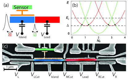
Figure 1(a) shows a schematic of the measurement configuration. The Coulomb blockaded superconducting island (blue) is capacitively coupled to an RF charge sensor (green) using a floating metallic coupler (yellow). The energy diagram of the superconducting island is shown in Fig. 1(b). The even-odd regime is characterized by alternating spacing between the charge degeneracies when . The superconducting island was tunnel coupled to a superconducting lead (red), fabricated on the same NW, ohmically connected to a normal-metal reservoir. Figure 1(c) shows a false-color micrograph of the device. The 100 nm diameter NW is grown using the vapor-liquid-solid technique in a molecular beam epitaxy system with the InAs [111] substrate crystal orientation. Following the NW growth, Al is deposited epitaxially in situ on three facets of the NW with an average thickness of 10 nm Krogstrup . The NW is then manually positioned on a chip with few-m precision. Using electron beam lithography and Transene D wet etch, the Al shell was removed from the nanowire near narrow gates denoted LCut, MCut, and RCut (cutters). Extended gates denoted L, Island, Lead, and R (plungers) tune the density in the corresponding segment of the NW Sole2018 ; deMoor2018 . In the measurement configuration, the voltage on gate LCut was set strongly negative such that tunneling to the island was controlled entirely by . Charge detection was performed using the capacitively coupled charge sensor with a 20 s integration time RazmadzePRN . During the counting experiment, the bias voltage across the superconducting island was set to zero, , thereby grounding the leads. The measurements were performed in a dilution refrigerator with a base temperature of 20 mK and a 1-1-6 T vector magnet.
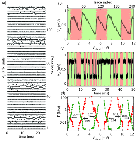
For all measurements, V, and was set positive to fully open the RCut junction. For charge-counting measurements, a single-lead Coulomb island was formed by setting strongly negative, disconnecting the left side of the island, while was set so that the normal-state conductance of MCut was 0.35 , checked via transport with LCut fully open. Typical charge sensing data for = 0 V are shown in Fig. 2(a), with each trace shifted for clarity. For each time trace, the demodulated reflectometry voltage was sampled at a fixed plunger voltage , then was stepped to the next value. Near charge degeneracies rapid tunnelings were observed, while away from transitions the switching vanished, reflecting stable charge configurations in Coulomb valleys. Averaging each time trace yielded a single average charge-sensor signal, which is plotted as a function of in Fig. 2(b). The moderate amount of even-odd spacing of the transitions suggest a charging energy eV, roughly twice the induced superconducting gap eV EilesPRL93 .
Figure 2(c) shows a time trace acquired with fixed near a charge degeneracy. The high signal-to-noise ratio of the sensor signal (SNR 3 SNR ) allowed the use of simple thresholding to determine transitions between odd and even occupations, color coded in Fig. 2(c), rather than more sophisticated thresholding techniques Ferguson17 ; PranceNano . Specifically, tunneling rates were determined from time traces like this by dividing the number of transitions out of a charge state, even or odd, , by the total time spent in that state within the time trace, MaisiPRL11 .
Resulting tunneling rates (green) and (red) are shown in Fig. 2(d). The two rates cross at each charge degeneracy, identifying both the value of where even and odd occupancies are equally likely, and the tunneling rate ( charge transition rate) at that transition, indicated by black arrows in Fig. 2(d).
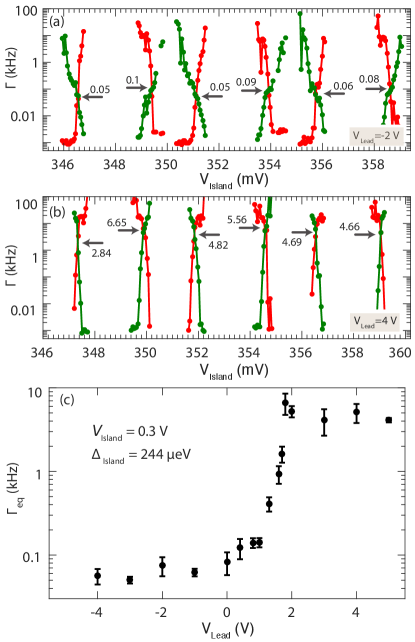
Motivated by Refs. AumentadoPRL04 ; PekolaAPL09 , which demonstrated that QPs are attracted to small-gap regions, we investigate how QP tunneling of the island depends on plunger voltage, , which can alter the induced gap of the nanowire lead. To do so, we associate the QP tunneling rate with the equilibrium (on resonance) tunneling rate, , found by averaging [green(red)] over several adjacent charge degeneracies [arrows in Figs. 2(d)] for fixed . Values for are determined in a similar manner for various values of .
Figures 3(a,b) show tunneling rates as drives the island through several Coulomb valleys for widely different lead plunger voltages, V and V. Because of unavoidable capacitive coupling of to the tunnel barrier, it is necessary to adjust in order to keep the effective tunnel barrier constant. Otherwise, changes in could simply reflect changes in the barrier transmission with changing . To compensate this cross-coupling, is adjusted whenever is changed, such that the normal state conductance for this barrier remains at using a separate transport measurement. For instance, in Fig. 3(a) V, and in Fig. 3(b) V. The average tunneling rate at crossing points is kHz for V, and Hz for V. In other words, the compensated increase of by 6 V between (a) and (b) increases the tunneling rate by two orders of magnitude without changing the normal-state resistance.
Figure 3(c) shows as is varied from V to V, with fixed near V and the middle cutter compensated using as described above. Resonances that depend on , presumably due to disorder in the middle-cutter junction, give rise to a non-monotonic dependence of tunneling with and corresponding non-monotonic normal state conductance as a function of . Before the counting experiment, we open and , and use transport measurement to verify that for each set of (, ) supp . Figure 3(c) shows a change in by two orders of magnitude when the difference between and is about 1 V. For larger gate-voltage differences, V, the tunneling rate saturates at a low and high value with little gate dependence.
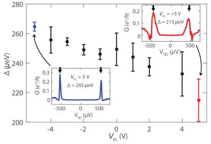
Previous experiments on similar NWs have demonstrated that the induced superconducting gap in the NW can be controlled by the plunger gate voltage ChangNNano . Our interpretation of the origin of the changes in with is that at more positive values of the superconducting gap is smaller on the lead than in the island, . In addition, as becomes more positive there is a softening of the induced superconducting gap. Both of these effects are evident in SIS transport measurements performed on the tunnel junction between the island and the lead. The distance between the two coherence peaks, marked by two black arrows in Fig. 4 insets, gives , where is the superconducting gap on the island (lead) side of the tunnel barrier. We set all plungers , , , and to the same value, denoted , and consider . Figure 4 shows the change in induced superconducting gap while varying . The induced superconducting gap decreases linearly from 270 to 210 eV as the plunger voltage is increased. This is because an increase in gate voltage increases the electron density in the semiconductor, which weakens the proximity effect induced from the ultrathin Al layer. Based on the data in Fig. 4, the drastic change in in Fig. 3(c) over a voltage range V corresponds to a change of superconducting gap of eV. This energy matches approximately the base temperature of our cryostat, suggesting that thermal smearing governs the cross-over from low to high tunneling rates in the observed .
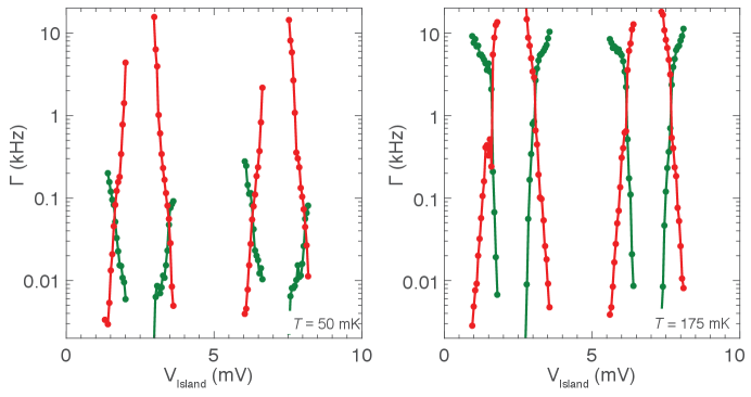
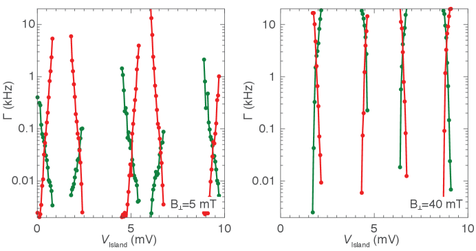
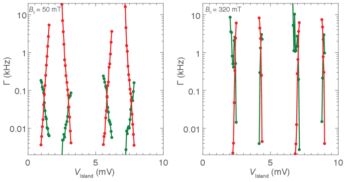
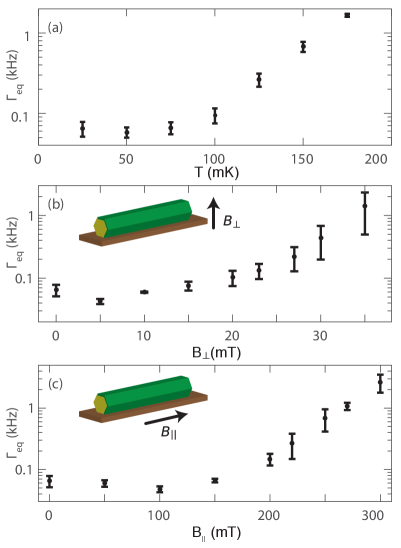
Single-charge tunneling rates were also investigated as a function of the temperature and magnetic field. Keeping the same gate configuration as in Fig. 2, we repeat the counting measurement. Inside a Coulomb valley, the charge state is always stable, similar to Fig. 2(a). Next, we focus on the tunneling rate at degeneracy as introduced above. increases with temperature [Fig. 5(a)] and magnetic field applied perpendicular to the substrate [Fig. 5(b)] and along the NW [Fig. 5(c)]. The increased rate as a function of these parameters is consistent with the softening and reduction of the induced superconducting gap leading to an enhancement of QP generation rates and . At the highest measured axial magnetic field value in Fig. 2(b), = 300 mT, the island changes its ground state configuration approximately every 300 s ( 3 kHz), similar to metallic devices MaisiPRL14 ; DelsingPRB08 ; ClarkPRB08 .
In summary, we investigated a gate-defined Coulomb island in the InAs/Al nanowire such that quasiparticles can only tunnel from one side of the island. Employing reflectometry, we count tunneling events on an island through that tunnel barrier in real time. Deep in the Coulomb valley the island shows no signal of quasiparticle tunneling on time scales ranging from sub-microsecond time scales to hours MannilaNPhys . At charge degeneracy points, the tunneling rate varies by orders of magnitude with electrostatic gating of the island (Fig. 3c) as well as the lead (Supplemental Fig. S1). We interpret the dependence as arising from the gate dependence of the relative sizes of the induced gaps in the island and lead Mannila ; AumentadoPRB06 ; FergusonPRL06 as well as the softness of the induced gaps. Tunneling rates also shows a strong dependence temperature and magnetic field, effects not yet modeled.
We thank Roman Lutchyn, Dmitry Pikulin, Judith Suter, and Jukka Vayrynen for valuable discussions, and Shiv Upadhyay for help with fabrication. Research is supported by Microsoft, the Danish National Research Foundation, and the European Research Commission, grant 716655, and a grant (Project 43951) from VILLUM FONDEN.
References
- (1) R. M. Lutchyn, E. P. A. M. Bakkers, L. P. Kouwenhoven, P. Krogstrup, C. M. Marcus, and Y. Oreg, Majorana zero modes in superconductor-semiconductor heterostructures, Nature Reviews Materials 3, 52 (2018).
- (2) Y. Oreg, G. Refael, and F. von Oppen, Helical Liquids and Majorana Bound States in Quantum Wires, Phys. Rev. Lett. 105, 177002 (2010).
- (3) R. M. Lutchyn, J. D. Sau, S. Das Sarma, Majorana fermions and a topological phase transition in semiconductor-superconductor heterostructures, Phys. Rev. Lett. 105, 077001 (2010).
- (4) V. Mourik, K. Zuo, S. M. Frolov, S. R. Plissard, E. P. A. M. Bakkers and L. P. Kouwenhoven, Signatures of Majorana Fermions in Hybrid Superconductor-Semiconductor Nanowire Devices, Science 336, 1003 (2012).
- (5) S. M. Albrecht, A. P. Higginbotham, M. Madsen, F. Kuemmeth, T. S. Jespersen, J. Nygård, P. Krogstrup, and C. M. Marcus, Exponential protection of zero modes in Majorana islands, Nature 531, 206 (2016).
- (6) J. Alicea, Y. Oreg, G. Refael, F. Von Oppen, and M. P. Fisher, Non-Abelian statistics and topological quantum information processing in 1D wire networks. Nature Physics 7, 412 (2011).
- (7) T. W. Larsen, K. D. Petersson, F. Kuemmeth, T. S. Jespersen, P. Krogstrup, J. Nygård, and C. M. Marcus, Semiconductor-nanowire-based superconducting qubit, Phys. Rev. Lett. 115, 127001 (2010).
- (8) G. de Lange, B. van Heck, A. Bruno, D. J. van Woerkom, A. Geresdi, S. R. Plissard, E. P. A. M. Bakkers, A. R. Akhmerov, and L. DiCarlo, Realization of microwave quantum circuits using hybrid superconducting-semiconducting nanowire Josephson elements, Phys. Rev. Lett. 105, 127002 (2015).
- (9) L. Casparis, M. R. Connolly, M. Kjaergaard, N. J. Pearson, A. Kringhøj, T. W. Larsen, F. Kuemmeth, T. Wang, C. Thomas, S. Gronin, G. C. Gardner, M. J. Manfra, C. M. Marcus, K. D. Petersson, Superconducting gatemon qubit based on a proximitized two-dimensional electron gas, Nature Nanotech 13, 915 (2018).
- (10) M. Hays, V. Fatemi, D. Bouman, J. Cerrillo, S. Diamond, K. Serniak, T. Connolly, P. Krogstrup, J. Nygård, A. L. Yeyati, A. Geresdi, and M. H. Devoret, Coherent manipulation of an Andreev spin qubit, Science 373, 430 (2021).
- (11) A. P. Higginbotham, S. M. Albrecht, G. Kiršanskas, W. Chang, F. Kuemmeth, P. Krogstrup, P., T. S. Jespersen, J. Nygård, K. Flensberg, and C .M. Marcus, Parity lifetime of bound states in a proximitized semiconductor nanowire, Nature Physics 11, 1017, 2015.
- (12) S. J. MacLeod, S. Kafanov, and J. P. Pekola, Periodicity in Al/Ti superconducting single electron transistors, Appl. Phys. Lett., 95, 052503 (2009).
- (13) J. Aumentado, M. W. Keller, M. H. Devoret and John M. Martinis, Nonequilibrium quasiparticles and periodicity in Single-Cooper-Pair Transistors, Phys. Rev. Lett. 92, 066802 (2004).
- (14) W. Chang, S. M. Albrecht, T. S. Jespersen, F. Kuemmeth, P. Krogstrup, J. Nygård and C. M. Marcus, Hard gap in epitaxial semiconductor-superconductor nanowires, Nature Nanotech. 10, 232 (2015).
- (15) A. J. Ferguson, N. A. Court, F. E. Hudson, and R. G. Clark, Microsecond resolution of quasiparticle tunneling in the single-Cooper-pair transistor, Phys. Rev. Lett. 97, 106603 (2006).
- (16) N. A. Court, A. J. Ferguson, R. Lutchyn, and R. G. Clark, Quantitative study of quasiparticle traps using the single-Cooper-pair transistor, Phys. Rev. B 77, 100501(R) (2008).
- (17) N. J. Lambert, A. A. Esmail, F. A. Pollock, M. Edwards, B. W. Lovett, and A. J. Ferguson, Microwave irradiation and quasiparticles in a superconducting double dot, Phys. Rev. B 95, 235413 (2017).
- (18) M. D. Shaw, R. M. Lutchyn, P. Delsing, and P. M. Echternach, Kinetics of nonequilibrium quasiparticle tunneling in superconducting charge qubits, Phys. Rev. B 78, 024503 (2008).
- (19) J. Bylander, T. Duty, and P. Delsing, Current measurement by real-time counting of single electrons, Nature, 434, 361 (2005).
- (20) V. F. Maisi, D. Kambly, C. Flindt, J. P. Pekola, Full Counting Statistics of Andreev Tunneling, Phys. Rev. Lett. 112, 036801 (2014).
- (21) O. Naaman and J. Aumentado, Time-domain measurement of quasiparticle tunneling rates in a single-Cooper-pair transistor, Phys. Rev. B 73, 172504 (2006).
- (22) G. C. Menard, F. K. Malinowski, D. Puglia, D. I. Pikulin, T. Karzig, B. Bauer, P. Krogstrup, and C. M. Marcus, Suppressing quasiparticle poisoning with a voltage-controlled filter, Phys. Rev. B 100, 165307 (2019).
- (23) D. Razmadze, D. Sabonis, F. K. Malinowski, G. C. Menard, S. Pauka, H. Q. Nguyen, D. M.T. van Zanten, E. C.T. O Farrell, J. Suter, P. Krogstrup, F. Kuemmeth, and C. M. Marcus, Radio-Frequency Methods for Majorana-Based Quantum Devices: Fast Charge Sensing and Phase-Diagram Mapping, Phys. Rev. Appl. 11, 064011 (2019).
- (24) D. J. van Woerkom, A. Geresdi and L. P. Kouwenhoven, One minute parity lifetime of a NbTiN Cooper-pair transistor, Nature Physics, 11, 547 (2015).
- (25) J. van Veen, A. Proutski, T. Karzig, D. Pikulin, R. Lutchyn, J. Nygård, P. Krogstrup, A. Geresdi, L. P. Kouwenhoven, and J. D. Watson, Magnetic field dependent quasiparticle dynamics of nanowire single Cooper pair transistors, Phys. Rev. B 98, 174502 (2018).
- (26) R. J. Schoelkopf, P. Wahlgren, A. A. Kozhevnikov, P. Delsing, and D. E. Prober, The radio frequency single electron transistor (RF-SET): a fast and ultrasensitive electrometer, Science 280, 1238 (1998).
- (27) P. Krogstrup, N. L. B. Ziino, W. Chang, S. M. Albrecht, M. H. Madsen, E. Johnson, J. Nygård, C. M. Marcus and T. S. Jespersen, Epitaxy of semiconductor-superconductor nanowires, Nature Materials, 14, 400 (2015).
- (28) S. Vaitieknas, M. T. Deng, J. Nygård, P. Krogstrup, C. M. Marcus. Effective g factor of subgap states in hybrid nanowires, Phys. Rev. 121 037703, (2018).
- (29) M. W. A. de Moor, J. D. S. Bommer, D. Xu, G. W. Winkler, A. E. Antipov, A. Bargerbos, G. Wang, N. van Loo, R. L. M. Op het Veld, S. Gazibegovic, D. Car, J. A. Logan, M. Pendharkar, J. Sue Lee, E. P. A. M. Bakkers, C. J. Palmstrøm, R. M. Lutchyn, L. P. Kouwenhoven, and H. Zhang, Electric field tunable superconductor semiconductor coupling in Majorana nanowires, New Journal of Physics, 20 103049 (2018).
- (30) T. M. Eiles, J. M. Martinis, and M. H. Devoret, Even-odd asymmetry of a superconductor revealed by the Coulomb blockade of Andreev reflection, Phys. Rev. Lett. 70, 1862 (1993).
- (31) The signal to noise ratio is defined as SNR = , with denotes the mean value and denotes the standard deviation of the data.
- (32) J. R. Prance, B. J. Van Bael, C. B. Simmons, D. E. Savage, M. G. Lagally, M. Friesen, S. N. Coppersmith and M. A. Eriksson, Identifying single electron charge sensor events using wavelet edge detection, Nanotechnology, 26, 215201 (2015).
- (33) V. F. Maisi, O. P. Saira, Yu A. Pashkin, J. S. Tsai, D. V. Averin, and J. P. Pekola, Real-Time Observation of Discrete Andreev Tunneling Events, Phys. Rev. Lett. 21, 217003 (2011).
- (34) To further rule out the effect of resonances associated with the middle cutter , we perform an extra counting measurement with a fixed , and change from open to closed. This data, presented in the Supplemental parts, confirms that there is a plateau for that depends weakly on the value of .
- (35) E. T. Mannila, P. Samuelsson, S. Simbierowicz, J. T. Peltonen, V. Vesterinen, L. Gronberg, J. Hassel, V. F. Maisi and J. P. Pekola, A superconductor free of quasiparticles for seconds, Nat. Physics (2021).
- (36) E. T. Mannila, V. F. Maisi, H. Q. Nguyen, C. M. Marcus, and J. P. Pekola, Detecting parity effect in a superconducting device in the presence of parity switches, Phys. Rev. B 100, 020502 (2019).
SUPPLEMENTARY MATERIAL
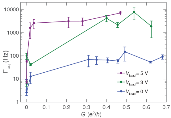
.1 Equilibrium poisoning rate as a function of
We repeat the quasiparticle counting experiment at different voltages on the lead gate as a function of cutter voltage . In Fig. S1, the poisoning rate is plotted as a function of high-bias conductance for three different lead voltages V, V, and V. When is set to negative voltages (closed), there is no electron tunneling into the island, as is also closed throughout the experiment. The time traces show a constant signal with no switching behavior. As is opened, the poisoning rate increases and quickly reaches a saturation plateau. The effect of disorder does not play a major role in the tunneling rate of electrons but introduces only local non-monotonicity in dependence on tunnel-barrier conductance . The plateau in Fig. 3(c) in the main text holds for a large voltage range on the cutter , and as a result allows the increase in the poisoning rate to be associated with the difference between and .
.2 Absence of quasiparticle poisoning as a function of temperature and fields
To emphasize the absence of quasiparticle poisoning in the hybrid InAs/Al island, we next present the study of tunneling rates as a function of the island plunger voltage when the device is in a similar configuration to Fig. 2 presented in the main text. For this study the voltage is again set to a very negative value such that the tunnelling rate to the left lead is negligible, whereas is set such that the high-bias conductance through the junction is and = 0 V. In all three experiments where we change temperature (Fig. S2), perpendicular magnetic field (Fig. S3), and parallel magnetic field (Fig. S4), the Coulomb valleys always show small tunnelling rates indicating that the island rarely changes its parity when deep in the Coulomb valley. At the charge degeneracy points a rate increase is observed when increasing temperature or magnetic field, consistent with the softening of the superconducting gap. For all three dependencies shown below the measurements were stopped when the tunneling rates became too fast to measure.