Electromagnetic evanescent field associated with surface acoustic wave:
Response of metallic thin films
Abstract
Surface acoustic waves (SAWs), coherent vibrational modes localized at solid surfaces, have been employed to manipulate and detect electronic and magnetic states in condensed-matter systems via strain. SAWs are commonly excited in a piezoelectric material, often the substrate. In such systems, SAWs not only generate strain but also electric field at the surface. Conventional analysis of the electric field accompanying the SAW invokes the electrostatic approximation, which may fall short in fully capturing its essential characteristics by neglecting the effect of the magnetic field. Here we study the electric and magnetic fields associated with SAWs without introducing the electrostatic approximation. The plane wave solution takes the form of an evanescent field that decays along the surface normal with a phase velocity equal to the speed of sound. If a metallic film is placed on the piezoelectric substrate, a time- and space-varying electric field permeates into the film with a decay length along the film normal defined by the skin depth and the SAW wavelength. For films with high conductivity, the phase of the electric field varies along the film normal. The emergence of the evanescent field is a direct consequence of dropping the electrostatic approximation, providing a simple but critical physical interpretation of the SAW-induced electromagnetic field.
I Introduction
Surface acoustic waves (SAWs), which are vibrational modes localized at the surfaces of solids, serve as distinctive tools for non-invasive manipulation and detection of the electronic states in condensed matter systems. Coherent excitation of SAWs is typically achieved by applying an rf signal to periodically spaced electrodes patterned on a piezoelectric substrate White and Voltmer (1965), which induces an accompanying ac electric field. This electric field mobilizes charge carriers within a conducting material positioned along the SAW’s delay line, while the back reaction alters the SAW’s amplitude and velocity Collins et al. (1968); Ingebrigtsen (1970); Ricco et al. (1985); Wixforth et al. (1986). Consequently, SAWs can be effectively employed as a contactless electrical probe operating in the microwave frequency range, offering a robust technique for tracking low-frequency conductivity Adler et al. (1981); Fritzsche (1984); Paalanen et al. (1992); Karl et al. (2000); Müller et al. (2005); Wu et al. (2024) and diagnosing quantum Hall states Efros and Galperin (1990); Fal’ko et al. (1993); Rotter et al. (1998); Fang et al. (2023). In addition, the SAW has attracted a growing interest in the field of spintronics as a source of rf mechanical motions that can interact with electron spins via magnetostriction Weiler et al. (2011); Dreher et al. (2012); Thevenard et al. (2014); Sasaki et al. (2017), or spin-vorticity coupling Matsuo et al. (2013); Kobayashi et al. (2017); Huang et al. (2023). Precise understanding of the SAW-induced electric field is thus of vital importance to distinguish electrical origins of the charge and spin dynamics from mechanical ones.
Conventional analysis of the electric field () typically employs the electrostatic approximation Tiersten (1963); Tseng and White (1967); Campbell and Jones (1968); Ingebrigtsen (1969, 1970), which introduces a scalar potential and sets . It also implies the absence of the time derivative of the magnetic field, being equivalent to neglecting the Ampère-Maxwell law. With regard to the analysis of SAW-induced electric fields, the approximation typically provides a quantitatively accurate description so far as the field amplitude is concerned since the phase velocity of the SAW () is about five orders of magnitude smaller than the speed of light (). However, it may be inadequate for fully capturing characteristics of the electric field, particularly in systems involving metallic films on piezoelectric substrates. First, the approximation can yield quantitatively different conclusions if additional small parameters, comparable to , are present in the system. Such parameters in the piezoelectric substrate/metal composite include the ratio of the Thomas-Fermi length (0.1 nm) to the SAW wavelength (1-10 m), and the ratio of displacement current to conduction current. Second, the neglectance of the electromagnetic induction can obscure the field screening mechanisms in conducting materials. The electric field associated with the SAW turns out to include a transverse component () and, according to the Faraday’s law, must induce an ac magnetic field. In metals, this magnetic field leads to the screening of electromagnetic waves via electric currents to satisfy the Ampère-Maxwell law, a phenomenon known as the skin effect; the penetration is characterized by the skin depth, which is typically several tens of micrometers for microwave frequency fields. Under the electrostatic approximation, however, the skin effect cannot be treated due to the absence of the magnetic field.
In this work, we study electric and magnetic fields associated with SAW without invoking the electrostatic approximation and identify the applicable conditions. We find that the SAW generates a transverse electric field, which can be considered as an electromagnetic evanescent wave that travels at the speed of sound, in addition to the conventional longitudinal electric field. We derive the decay length of the former, which is determined by the SAW wavelength and the skin depth. For films with large conductivity and thickness, the distribution of the electric field inside the film is a quantitatively different from that under the electrostatic approximation. The electrostatic approximation is justified when the skin depth is sufficiently larger than the SAW wavelength, which is not necessarily always the case for metallic films. This work bridges the gap between the general framework for the electromagnetic response of metallic films and the simplified treatment under the electrostatic approximation commonly employed in SAW studies, offering a clear and straightforward physical interpretation of the SAW-induced electric field.
II Setup
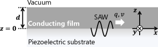
We are primarily concerned with plane wave propagation along the interface between a piezoelectric substrate and a (nonmagnetic) conducting layer of thickness facing vacuum. Let the coordinate system be oriented such that the wave propagates along and the substrate occupies as shown in Fig. 1. We would like to know the electromagnetic waves described by the macroscopic Maxwell’s equations,
| (1) | |||||
| (2) | |||||
| (3) | |||||
| (4) |
where denote the free charge density and current density, respectively. Different material media are distinguished by the constitutive relations between and as well as the assumptions on the free charges. We model each region as follows:
- Vacuum ()
-
(5) where are the permittivity and permeability of vacuum respectively.
- Conducting slab ()
-
(6) where are the relative permittivity, conductivity, and the diffusion constant.
- Piezoelectric substrate ()
-
(7) where is the dielectric tensor, and is the electric polarization associated with the linear strain tensor through the piezoelectric tensor . The displacement vector , related to the strain by , obeys the equation of motion,
(8) where is the mass density of the piezoelectric substrate and is the elastic stiffness tensor. Repeated Latin indices are understood to be summed over.
Since all the equations involved are linear, the solutions can be sought in the form where and are the in-plane wavenumber and phase velocity, respectively. To avoid notational mess, we hereafter understand all the dependent variables are of this form and suppress the appearance of . Under our assumption that holds everywhere, we can eliminate and via Eqs. (1) and (2),
| (9) |
Note that Eq. (2) is redundant for . From Eqs. (1) and (3), one obtains
| (10) |
We again note that the constraint Eq. (4) becomes redundant for because and satisfy the conservation law. The equations are supplemented by boundary conditions appropriate for different material interfaces. In the following, we first solve the equations in each region with a boundary condition if it can be discussed independently of the other regions. We then glue the solutions together at the interfaces by imposing the remaining boundary conditions.
III Solution in each region
In this section, we solve Eq. (LABEL:eq:TM_TE) in each region separately. The obtained solutions will be conjoined by the electromagnetic boundary conditions in the next section.
III.1 Vacuum half-space
First we consider the vacuum half-space (). We demonstrate that the evanescent field is a universal feature of vacuum electromagnetic waves forced to propagate slower than the speed of light . Noting , Eq. (LABEL:eq:TM_TE) yields
| (11) |
Imposing the vanishing boundary condition at , one obtains from Eq. (11),
| (12) | |||||
| (13) |
where is the Lorentz factor, and we assume in the following. The integration constants, and , will be determined by the boundary conditions at . Equations (12) and (13) represent the transverse magnetic (TM) and the transverse electric (TE) modes, respectively.
The above solution has been derived independently of the boundary conditions at . This shows that any electromagnetic waves in vacuum that decay at infinity automatically take the form of the evanescent wave Bliokh et al. (2014), as pointed out for the special case of the Bleustein-Glyaev type SAW Bleustein (1968); Gulyaev (1969) in highly symmetric piezoelectric materials Li (1996). As an example, the TM mode Eq. (12) is schematically illustrated in Fig. 2. The electric and magnetic field lines display the presence of an electromagnetic field associated with the SAW. Note that going beyond the electrostatic approximation predicts a nonzero magnetic field, hence the transverse component of the electric field, associated with the SAW. Although the magnetic field component is significantly smaller compared to the free electromagnetic field, this result can potentially be relevant because it directly couples to electron spin and magnetization Jiang et al. (2023); Kline et al. (2024).
III.2 Conducting slab
Next we consider the solution inside a conducting slab. We assume that the conductor is isotropic, and introduce the reduced speed of light , the skin depth , and the Thomas-Fermi length . One then obtains
| (14) |
with
| (15) |
The general solutions are written in the form,
| (16) |
where , , and
| (17) | ||||
with
| (18) | |||||
| (19) | |||||
| (20) |
whereas the other components vanish, . Thus, the electric field consists of TM, TE, and longitudinal components with two integration constants each. Note that represents the ratio of displacement current () to drift current (), which is several orders of magnitude smaller than unity in metals for microwave frequency field. For later use, we give electric current density and charge density,
| (21) |
| (22) |
Without relying on the electrostatic approximation, we have obtained the precise decay length of the transverse components, Eq. (18), which explicitly takes the skin effect into account. Equation (18) reproduces the previous result Ingebrigtsen (1970) if we neglect the skin effect () and take the limit , whereas it reduces to the ordinary skin effect if we set . Since the SAW velocity is about five orders of magnitude smaller than the speed of light, is always satisfied. Thus the difference between the updated [Eq. (18)] and the conventional one Ingebrigtsen (1970) comes from the imaginary term under the square root. The derived expression suggests that the contribution of the skin effect cannot be neglected when is comparable to and in such a case it predicts a shorter decay length than the conventional model. Such a situation occurs in materials with sufficiently large conductivity and thus the result obtained here can be important especially for metallic films.
Let us proceed to discuss the boundary conditions that can be imposed independently of the other regions. Equation (17) has six integration constants corresponding to three dynamical degrees of freedom; two for photons and another for conduction electrons. Two of the constants can be eliminated by imposing at the boundaries, enabling one to express in terms of ;
| (23) |
Thus the general solutions in the conducting slab have four constants to be determined by the electromagnetic boundary conditions. At this stage, one already sees that the ratio is roughly equal to . This is a robust consequence of the current conservation at the boundaries and holds irrespective of the materials outside as long as they are insulating. Then, from Eq. (21), the ratio of the in-plane current induced by the longitudinal field to that by the transverse field is . As explicitly shown in Sec. VI, there typically exists a hierarchy , so that the in-plane current is induced mostly by the transverse field. As for the electric field [Eq. (17)], the longitudinal component dominates near the interface whereas the transverse one decays slower and becomes prominent in relative terms into the depth of the metal, which is a different behavior from the electric current. This is because the electric current contains the diffusive component induced by the charge accumulation in addition to the drift current proportional to the electric field. Note that these estimates can be easily confirmed for films of infinite thickness, where , and
| (24) |
| (25) |
III.3 Half-infinite piezoelectric substrate
In general, the analytical solutions for this case () are either unavailable or intractable mainly because the system intrinsically lacks rotational symmetry. Since our model ignores mechanical degrees of freedom in the conductor, the electromagnetic field inside the piezoelectric substrate affects the conducting slabs only via the boundary conditions, i.e., the amplitudes of the electric and magnetic fields at . Taking advantage of this, we merely outline the framework of the numerical calculation here, avoiding the actual evaluation of the electromagnetic field and treating their interface values as input parameters in the later analysis.
The solutions can be computed by simultaneously solving Eqs. (8) and (LABEL:eq:TM_TE) under the constraints Eqs. (4) and (7) and given boundary conditions Tiersten (1963); Tseng and White (1967); Campbell and Jones (1968); Ingebrigtsen (1969). Eliminating by Eq. (7), there exist six unknown functions, and , governed by the six time-evolution equations (8) and (LABEL:eq:TM_TE) with one constraint Eq. (4), implying five dynamical degrees of freedom. The equations are explicitly shown in Eq. (41) in Appendix IX.1, which do not contain the second order derivative of with respect to . This makes it harder to determine the order of the equations in , or the number of the integration constants. One may thus algebraically eliminate and from the seven equations (Eqs. (8), (LABEL:eq:TM_TE), and Eq. (4)) and obtain five equations of second order in for five dependent variables (, and ), which yields ten integration constants. The number is reduced by half by demanding either exponential decay towards Ingebrigtsen and Tonning (1969). The stress-free boundary condition, i.e., the vanishment of the stress normal to the substrate surface, should be able to eliminate three of the five remaining constants, leaving two to be determined through the electromagnetic boundary conditions, which in fact encode the information of the adjoining medium, i.e., the conductor facing vacuum in our case.
IV Solutions for the full film stack
Now we are in a position to glue the solutions obtained above together by the electromagnetic boundary conditions. To guide the calculations, we first review the structure of the present boundary value problem. Per interface, there are six boundary conditions that follow from Maxwell’s equations (continuity of tangential and normal ), only four of which are independent. This can be understood as follows. If all the field components are independent of , the -components of Eqs. (1) and (3),
| (26) |
together with the plane-wave ansatz , and the metal-insulator boundary condition lead to
| (27) |
at the boundaries. Thus, the continuity of is equivalent to that of , leaving four independent conditions for each boundary ( and ). In the present system, the eight conditions are imposed on the eight integration constants; and in vacuum, and in the conducting slab, and the remaining two in the piezoelectric substrate. As have been represented by [Eq. (23)], they are not included here. Note that the SAW’s phase velocity is also a parameter that must be determined. The above conditions contain as a parameter, and we numerically look for a value of that satisfies all conditions. Through this process, the eight integration constants are determined up to an overall multiplicative factor representing the SAW amplitude, which should be assigned by the external force to excite the SAW, e.g. the input power to the interdigital transducer.
The above procedure allows one to obtain a numerical solution for a specific stack, provided that the material constants of the piezoelectric substrate and the film are known. To obtain an analytical expression, however, is a heavy burden due to the low crystal symmetry of the substrate. As our interest here is the general behavior of the electric current and charge in the metallic film, here we assume that the parameters associated with the substrate are given and seek to provide an explicit form for and . We therefore regard and the amplitudes,
| (28) |
as given and fixed. and , the electric field amplitude at the film/substrate interface, are later used as units for the TM and TE mode amplitudes in the conducting slab, respectively. The two parameters are in general coupled and an additional relationship arises between and . Thus one may set either or as given and express and in units of the other. However, the analytical expression of the relation, which is obtained from the boundary condition at (see Appendix, Sec. IX.2), is prohibitively complicated and we proceed with two fixed constants, and .
Let us consider the boundary at between the vacuum and conductor. Two of the four boundary conditions can be used to eliminate and the remaining two impose conditions among and . As a result, one obtains the following two equations on :
| (29) |
| (30) |
where can be expressed with via Eq. (23). We remark that these equations are equivalent to the continuity of surface impedances and across the boundary. Equations (29) and (30), together with (23), offer four conditions among six constants , , and , which we choose to represent through two auxiliary constants, and , as
| (31) | |||||
| (32) | |||||
| (33) |
Next we move on to the boundary at . Looking at Eqs. (17) and (31) - (33), the continuity of at is sufficient to determine and in terms of and ,
| (34) | ||||
This achieves our goal of expressing the electromagnetic field and current in the conducting slab between vacuum and substrate in terms of tangential electric fields at the substrate/film interface. We reiterate that the remaining boundary conditions, i.e., the continuity of and at , can be used to determine and the relative amplitude between and , though we would not carry it out here (see Appendix IX.2 for the detail). Instead, we employ these results to evaluate the electric current and charge distribution within a metallic film.
V Electrostatic limit
V.1 Definition of the electrostatic approximation
Let us discuss the relation between the results described above and those obtained from the electrostatic approximation. First, we comment on the definition of the electrostatic approximation. It is often the case that one neglects the time derivative of . Setting in Eq. (1) leads to , which allows one to use . However, Eq. (3) does not exactly hold when : substituting into the time derivative of Eq. (3) multiplied by reads
| (35) |
This is the requirement to justify the electrostatic approximation. When , and in Eq. (17) are plugged into Eq. (35), one obtains
| (36) |
Equation (36) shows that we must assume together with to uphold Eq. (3) under . We therefore define the electrostatic approximation as and , where the latter emerges from substituting the former into Eq. (1). Indeed, this is the approach taken by Ingebrigtsen Ingebrigtsen (1970). The sufficient conditions to uphold all the Maxwell equations under the electrostatic approximation are and . Note that is independent of . For the case under interest here, the former is of the order unity while the latter is small, providing an example where is not a sufficient condition to justify the electrostatic approximation.
V.2 Connection to the electrostatic limit
Here we remark on how our results fit into the electrostatic approximation.
The electric field is then purely longitudinal, which should be screened by free charges and cannot penetrate into the conductor beyond the electrostatic screening length (). This apparently contradicts our results [Eq. (17)] in which the transverse component remains nonzero and unscreened up to a much larger distance even in the electrostatic limit. To resolve this puzzle, one should carefully distinguish two possible definitions of the longitudinal and transverse components. Namely, one may call () longitudinal (transverse) if
(i) (),
or if
(ii) ().
So far, we have used (i) to classify longitudinal and transverse fields, which conforms with the terminology often used.
However, (ii) is better adapted in the screening argument as it is the condition for generating the screening charges and currents through the Gauss’ and Ampère-Maxwell law, respectively.
The difference between the two definitions is usually immaterial, but it does matter when and , i.e., when is a harmonic function. Such a harmonic qualifies to be longitudinal as well as transverse under (i), whereas it is neither of them according to (ii).
It turns out that in Eq. (17) is exactly the harmonic under the electrostatic approximation.
That is, satisfies both and as .
Thus is longitudinal by (i) but is not by (ii).
If we were to use (ii), it is reasonable to have that penetrates deep into the conductor with a decay length of .
Note that abandoning the electrostatic approximation removes such ambiguity: the longitudinal and transverse components are clearly distinguished (there is no equivalent harmonic component) and they are respectively screened by induced charges and currents.
VI Quantitative estimation
In this section, we calculate the profile of the electric current and charge density in metallic films. First, we compare the profile calculated with and without the electrostatic approximation. For this purpose, the electrical conductivity of the film is set large such that the condition for the electrostatic approximation, , does not hold. Next, we model a system in which SAW-induced spin current was observed experimentally. Material parameters that match the experimental conditions are used. We discuss the consequence of the results obtained here on the SAW-induced spin current.
As noted in the previous section, we regard as given and use the value of Y-cut LiNbO3, m/s Datta (1986).
In the following, we also assume and m-1. The diffusion coefficient is chosen to be , a representative value for metals Maekawa et al. (2017); Niimi et al. (2013). With these parameters, we obtain nm and . The latter satisfies one of the sufficient conditions for the electrostatic approximation, .
VI.1 Difference with the electrostatic approximation
As shown in Section III.2, calculations with and without the electrostatic approximation provide quantitatively different results unless .
To see this, we estimate the distribution of the electric current in films with large electrical conductivity: m. With these parameters, , and m. Consequently, we have that violates the condition for the electrostatic approximation.
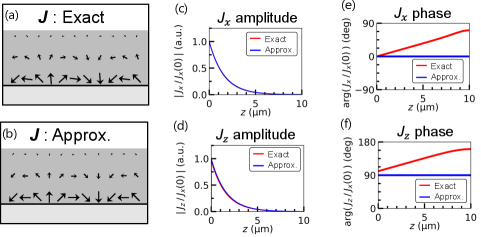
Figure 3 shows the profiles of the electric current density profiles with and without the electrostatic approximation. The solutions under the approximation are obtained by substituting and into those without it. We set the film thickness m to display the changes along the -axis. Without the approximation, the electric current changes its phase monotonically along the -axis whereas the phase remains constant under the approximation This is caused by the imaginary part of [Eq. (18)], which is not negligible for films with large conductivity. As is evident from the plots shown in Fig. 3(a,b), the phase change manifests itself in the current flow distribution along the -axis. At a given position in the - plane, the current changes its direction as one moves along the -axis when the electrostatic approximation is abandoned, whereas the direction remains the same throughout the entire film when the approximation is maintained.
VI.2 Modeling of an experimental setup
Next, we model an experimental setup in which SAW-induced spin current was foundKawada et al. (2021). In accordance with the experiments, the film conductivity and thickness are set to and nm, respectively; however, qualitatively similar results are obtained as long as nm. These parameters return , and m. Thus , allowing one to use the electrostatic approximation. However, here we do not apply the approximation and follow the discussion described above.
From the parameters defined above, and hold so that , , . Therefore, Eq. (34) is well approximated by
| (37) |
Note that cannot be set to zero even at this leading order. Using the same approximations, one obtains
| (38) | |||||
| (39) |
As shown in Eqs. (21) and (22), is effectively screened by the small factor while remains sizable in the film. Therefore, the charge current inside metal is completely dominated by the transverse contribution whereas the charge density is mostly induced by . We note that is consistent with as the smallness of is a result of cancellation between the and terms; such cancellation is absent in the derivative because of the sign change of the latter term.
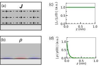
The uniformity of the electric current and the localization of the charge density within the metallic thin film are directly demonstrated by evaluating Eqs. (21) and (22) using Eq. (17). The results are schematically illustrated in Fig. 4 (a) and (b). Due to the small factor of originating from the electrostatic screening, the longitudinal components of that originates from localized at the film surfaces become negligibly small. In addition, cancellation between and results in a significant decrease of overall. The charge density is confined at the interface between the substrate and film to screen out coming from the substrate. To illustrate the distribution along more quantitatively, the absolute values of and are plotted against in Fig. 4 (c) and (d). We see that is almost uniform along in the whole film and is concentrated within the range of the Thomas-Fermi length from the substrate surface.
Recent experimental work has demonstrated that SAWs induce an ac spin current in metallic thin films with significant spin-orbit interaction, an effect referred to as the acoustic spin Hall effect Kawada et al. (2021). The observed spin current flows parallel to the surface normal with its polarization orthogonal to both the flow and SAW propagation directions, and is distributed uniformly across the film thickness direction. Under the assumption that electric fields are efficiently screened by conduction electrons and decay rapidly in metals, the latter feature suggests that the spin current should have a mechanical origin rather than electromagentic one. From this work, however, we conclude that the SAW-induced electric field generates an electric current uniformly in the thickness direction in metallic thin films. This allows the uniform spin current to flow in strong spin orbit metals via the spin Hall effect, which can reasonably explain the microscopic origin of the acoustic spin Hall effect.
VII Conclusion
In summary, we have studied the electromagnetic response of a metallic thin film to the electric field associated with the piezoelectrically excited surface acoustic wave (SAW) without employing the electrostatic approximation. The electromagnetic field accompanying the SAW contains a component that behaves as an evanescent field and carries a transverse field, which is not screened by the electric charge but via the skin effect inside conductors. We refined the decay length of the SAW-induced electric field in conducting slabs, and found that it is determined by both the SAW wavelength and the skin depth. The electromagnetic evanescent field that accompanies SAW can therefore influence the transport properties of metallic thin films deposited on piezoelectric substrates, a playground for studies on acoustoelectronics and spintronics.
VIII Acknowledgements
We acknowledge fruitful discussions with K. Usami. This work was partly supported by JSPS KAKENHI (Grant Nos. 20J21915, 20J20952, 21K13886, 23KJ1419, 23KJ1159, 23H05463, and 24K00576), JST PRESTO Grant No. JPMHPR20LB, Japan, and JSPS Bilateral Program Number JPJSBP120245708.
IX Appendix
IX.1 Explicit form for half-infinite piezoelectric substrate
Here we explicitly describe equations for SAWs in a piezoelectric substrate. To emphasise the algebraic structure, let us introduce three-by-three matrices
| (40) |
Equations (8) and (LABEL:eq:TM_TE) under the constraints Eqs. (4) and (7) can be written as
| (41) | ||||
| (42) |
where is the three-by-three unit matrix and
| (43) |
Since Eq. (41) does not contain second order derivative on , the mathematical structure of the problem is harder to see than the other cases. One formal approach is to eliminate and by using the last of Eq. (41) and Eq. (42), which should leave an equation for of second order in . Although this procedure cannot be used to eliminate when , it is applicable for the Rayleigh-type SAW, the system of our interest. Then, one expects to obtain five independent solutions of the form , and the stress-free boundary condition
| (44) |
should be able to eliminate three of the five arbitrary constants, leaving two to be determined through the electromagnetic boundary conditions.
IX.2 Surface impedance at substrate/film interface
In the main text, we expressed the electric field inside the conducting slab in terms of the electric field at the substrate/film interface. As we mentioned in the last paragraph of Sec. IV, obtaining and the relative amplitude between and requires the continuity of and at . The conditions are equivalent to equating the surface impedance of both sides, as described by Refs. Ingebrigtsen (1969, 1970). The surface impedance is defined in each region independently. We first derive the analytical formula of the surface impedances in the conducting slab, which read
| (45) | ||||
From Eqs. (31) and (32), one obtains the surface impedance for the conducting slab as
| (46) |
| (47) |
agrees with the expression given in Ref. Ingebrigtsen (1970) when setting and . The expression of can be derived only when the electrostatic approximation is not employed. Assuming is neither very small nor large, involves two small parameters; and . In any case, the dominant contributions arise from the terms proportional to in both the numerator and denominator. We also remark that the limit implies , which yields a well-defined limit and consistent with the so-called shorted boundary condition Campbell and Jones (1968).
Next we outline how the surface impedance of the adjoining piezoelectric medium can be obtained. The general structure of the bulk solution of the electromagnetic fields can be inferred as discussed in Sec. III.3. This solution should contain two arbitrary constants that characterize it (for instance, and ), allowing for the numerical computation of the surface impedance , on the side if the value of is determined.
References
- White and Voltmer (1965) R. M. White and F. W. Voltmer, “Direct piezoelectric coupling to surface elastic waves,” Appl. Phys. Lett. 7, 314 (1965).
- Collins et al. (1968) J. H. Collins, K. M. Lakin, C. F. Quate, and H. J. Shaw, “Amplification of Acoustic Surface Waves with Adjacent Semiconductor and Piezoelectric Crystals,” Applied Physics Letters 13, 314–316 (1968).
- Ingebrigtsen (1970) K. A. Ingebrigtsen, “Linear and nonlinear attenuation of acoustic surface waves in a piezoelectric coated with a semiconducting film,” J. Appl. Phys. 41, 454 (1970).
- Ricco et al. (1985) A.J. Ricco, S.J. Martin, and T.E. Zipperian, “Surface acoustic wave gas sensor based on film conductivity changes,” Sensors and Actuators 8, 319–333 (1985).
- Wixforth et al. (1986) Achim Wixforth, Jörg P Kotthaus, and G Weimann, “Quantum oscillations in the surface-acoustic-wave attenuation caused by a two-dimensional electron system,” Physical review letters 56, 2104 (1986).
- Adler et al. (1981) R. Adler, D. Janes, B. J. Hunsinger, and S. Datta, “Acoustoelectric measurement of low carrier mobilities in highly resistive films,” Applied Physics Letters 38, 102–103 (1981).
- Fritzsche (1984) H. Fritzsche, “Analysis of the traveling-wave technique for measuring mobilities in low-conductivity semiconductors,” Phys. Rev. B 29, 6672–6678 (1984).
- Paalanen et al. (1992) M. A. Paalanen, R. L. Willett, P. B. Littlewood, R. R. Ruel, K. W. West, L. N. Pfeiffer, and D. J. Bishop, “rf conductivity of a two-dimensional electron system at small landau-level filling factors,” Phys. Rev. B 45, 11342–11345 (1992).
- Karl et al. (2000) Norbert Karl, Karl-Heinz Kraft, and Jörg Marktanner, “Charge carrier mobilities in dark-conductive organic thin films determined by the surface acoustoelectric travelling wave (saw) technique,” Synthetic Metals 109, 181–188 (2000).
- Müller et al. (2005) C. Müller, A. A. Nateprov, G. Obermeier, M. Klemm, R. Tidecks, A. Wixforth, and S. Horn, “Surface acoustic wave investigations of the metal-to-insulator transition of V2O3 thin films on lithium niobate,” Journal of Applied Physics 98, 084111 (2005).
- Wu et al. (2024) Mengmeng Wu, Xiao Liu, Renfei Wang, Yoon Jang Chung, Adbhut Gupta, Kirk W. Baldwin, Loren Pfeiffer, Xi Lin, and Yang Liu, “Probing quantum phases in ultra-high-mobility two-dimensional electron systems using surface acoustic waves,” Phys. Rev. Lett. 132, 076501 (2024).
- Efros and Galperin (1990) A. L. Efros and Yu. M. Galperin, “Quantization of the acoustoelectric current in a two-dimensional electron system in a strong magnetic field,” Phys. Rev. Lett. 64, 1959–1962 (1990).
- Fal’ko et al. (1993) Vladimir I. Fal’ko, S. V. Meshkov, and S. V. Iordanskii, “Acoustoelectric drag effect in the two-dimensional electron gas at strong magnetic field,” Phys. Rev. B 47, 9910–9912 (1993).
- Rotter et al. (1998) M. Rotter, A. Wixforth, W. Ruile, D. Bernklau, and H. Riechert, “Giant acoustoelectric effect in GaAs/LiNbO3 hybrids,” Appl. Phys. Lett. 73, 2128–2130 (1998).
- Fang et al. (2023) Yawen Fang, Yang Xu, Kaifei Kang, Benyamin Davaji, Kenji Watanabe, Takashi Taniguchi, Amit Lal, Kin Fai Mak, Jie Shan, and BJ Ramshaw, “Quantum oscillations in graphene using surface acoustic wave resonators,” Physical Review Letters 130, 246201 (2023).
- Weiler et al. (2011) M. Weiler, L. Dreher, C. Heeg, H. Huebl, R. Gross, M. S. Brandt, and S. T. B. Goennenwein, “Elastically driven ferromagnetic resonance in nickel thin films,” Phys. Rev. Lett. 106, 117601 (2011).
- Dreher et al. (2012) L. Dreher, M. Weiler, M. Pernpeintner, H. Huebl, R. Gross, M. S. Brandt, and S. T. B. Goennenwein, “Surface acoustic wave driven ferromagnetic resonance in nickel thin films: Theory and experiment,” Phys. Rev. B 86, 134415 (2012).
- Thevenard et al. (2014) L. Thevenard, C. Gourdon, J. Y. Prieur, H. J. von Bardeleben, S. Vincent, L. Becerra, L. Largeau, and J. Y. Duquesne, “Surface-acoustic-wave-driven ferromagnetic resonance in (Ga,Mn)(As,P) epilayers,” Phys. Rev. B 90, 094401 (2014).
- Sasaki et al. (2017) R. Sasaki, Y. Nii, Y. Iguchi, and Y. Onose, “Nonreciprocal propagation of surface acoustic wave in Ni/LiNbO3,” Phys. Rev. B 95, 020407 (2017).
- Matsuo et al. (2013) Mamoru Matsuo, Jun’ichi Ieda, Kazuya Harii, Eiji Saitoh, and Sadamichi Maekawa, “Mechanical generation of spin current by spin-rotation coupling,” Phys. Rev. B 87, 180402 (2013).
- Kobayashi et al. (2017) D. Kobayashi, T. Yoshikawa, M. Matsuo, R. Iguchi, S. Maekawa, E. Saitoh, and Y. Nozaki, “Spin current generation using a surface acoustic wave generated via spin-rotation coupling,” Phys. Rev. Lett. 119, 077202 (2017).
- Huang et al. (2023) Mingxian Huang, Wenbin Hu, Huaiwu Zhang, and Feiming Bai, “Giant coupling excited by shear-horizontal surface acoustic waves,” Phys. Rev. B 107, 134401 (2023).
- Tiersten (1963) H. F. Tiersten, “Wave propagation in an infinite piezoelectric plate,” Journal of the Acoustical Society of America 35, 234 (1963).
- Tseng and White (1967) Chin‐Chong Tseng and R. M. White, “Propagation of piezoelectric and elastic surface waves on the basal plane of hexagonal piezoelectric crystals,” J. Appl. Phys. 38, 4274–4280 (1967).
- Campbell and Jones (1968) J. J. Campbell and W. R. Jones, “A method for estimating optimal crystal cuts and propagation directions for excitation of piezoelectric surface waves,” IEEE Transactions on Sonics and Ultrasonics SU15, 209 (1968).
- Ingebrigtsen (1969) K. A. Ingebrigtsen, “Surface waves in piezoelectrics,” J. Appl. Phys. 40, 2681 (1969).
- Bliokh et al. (2014) Konstantin Y. Bliokh, Aleksandr Y. Bekshaev, and Franco Nori, “Extraordinary momentum and spin in evanescent waves,” Nat. Commun. 5, 3300 (2014).
- Bleustein (1968) J. L. Bleustein, “A new surface wave in piezoelectric materials,” Appl. Phys. Lett. 13, 412 (1968).
- Gulyaev (1969) Y. V. Gulyaev, “Electroacoustic surface waves in solids,” JETP Lett. 9, 37 (1969).
- Li (1996) S. F. Li, “The electromagneto-acoustic surface wave in a piezoelectric medium: The Bleustein-Gulyaev mode,” J. Appl. Phys. 80, 5264 (1996).
- Jiang et al. (2023) Zhengzhi Jiang, Hongbing Cai, Robert Cernansky, Xiaogang Liu, and Weibo Gao, “Quantum sensing of radio-frequency signal with NV centers in SiC,” Sci. Adv. 9, eadg2080 (2023).
- Kline et al. (2024) Cecile Skoryna Kline, Jorge Monroy-Ruz, and Krishna C Balram, “Piezoelectric microresonators for sensitive spin detection,” arXiv:2405.02212 (2024).
- Ingebrigtsen and Tonning (1969) K. A. Ingebrigtsen and A. Tonning, “Elastic surface waves in crystals,” Physical Review 184, 942–951 (1969).
- Datta (1986) S. Datta, Surface Acoustic Wave Devices (Prentice-Hall, 1986).
- Maekawa et al. (2017) Sadamichi Maekawa, Sergio O. Valenzuela, Eiji Saitoh, and Takashi Kimura, Spin Current (Oxford University Press, 2017).
- Niimi et al. (2013) Yasuhiro Niimi, Dahai Wei, Hiroshi Idzuchi, Taro Wakamura, Takeo Kato, and YoshiChika Otani, “Experimental verification of comparability between spin-orbit and spin-diffusion lengths,” Phys. Rev. Lett. 110, 016805 (2013).
- Kawada et al. (2021) T. Kawada, M. Kawaguchi, T. Funato, H. Kohno, and M. Hayashi, “Acoustic spin Hall effect in strong spin-orbit metals,” Science Advances 7, eabd9697 (2021).