This paper was converted on www.awesomepapers.org from LaTeX by an anonymous user.
Want to know more? Visit the Converter page.


Effects of valley splitting on resonant-tunneling readout of spin qubits

Tetsufumi Tanamoto Department of Information and Electronic Engineering, Teikyo University, Toyosatodai, Utsunomiya 320-8511, Japan [email protected]    Keiji Ono Advanced device laboratory, RIKEN, Wako-shi, Saitama 351-0198, Japan
Abstract

The effect of valley splitting on the readout of qubit states is theoretically investigated in a three-quantum-dot (QD) system. A single unit of the three-QD system consists of qubit-QDs and a channel-QD that is connected to a conventional transistor. The nonlinear source–drain current characteristics under resonant-tunneling effects are used to distinguish different qubit states. Using nonequilibrium Green functions, the current formula for the three-QD system is derived when each QD has two valley energy levels. Two valley states in each QD are considered to be affected by variations in the fabrication process. We found that when valley splitting is smaller than Zeeman splitting, the current nonlinearity can improve the readout, provided that the nonuniformity of the valley energy levels is small. Conversely, when the valley splitting is larger than the Zeeman splitting, the nonuniformity degraded the readout. In both cases, we showed that there are regions where the measurement time tmeast_{\rm meas} is much less than the decoherence time tdect_{\rm dec} such that tdec/tmeas>100t_{\rm dec}/t_{\rm meas}>100. This suggests that less than 1% measurement error is anticipated, which opens up the possibility for implementing surface codes even in the presence of valley splitting.

I Introduction

Background— Quantum computers have undergone rapid developments, targeting near-future applicationsGoogle2023 ; IBM2023 ; Fowler . In this respect, silicon qubits have attracted attention because of their affinity to advanced semiconductor circuits, which leads to the integration of qubits to build surface codes and control complementary metal-oxide semiconductor (CMOS) circuits on the same chip Loss ; Zwanenburg . At present, advanced commercial transistors have entered the 2-nm gate-length generation with three-dimensional stacked structures TSMC2023 ; Intel2023 ; IMEC2023 ; Kim ; Ryckaert . Because quantum effects become more prominent as the device size decreases, semiconductor qubits can get the most benefit from advanced semiconductor technologies Michniewicz .

Readout of spin qubits—The reading out of qubit states is one of the most important process to control the qubit. The Elzerman readout Elzerman , which is currently a mainstream for silicon qubits, uses a Zeeman-split spin 1/2 electron in a quantum dot (QD) as the qubit. The experimental setup of the Elzerman readout consists of a QD, an electrode (reservoir) weakly tunnel-coupled to the QD, and a charge sensor that monitors the charge state of the QD Koch ; Keith . The charge sensor detects the spin-dependent charge transfer between the QD and the electrode. However, this setup of the electrodes and the charge sensor for each qubit requires a large circuit area, when the qubits are integrated. In addition, each electrode and charge sensor requires multiple wiring, so the wiring circuitry is inevitably complex. These are factors that limit the large-scale integration of qubits with the Elzerman readout.

Regarding this readout process, we proposed a different method, a resonant-tunneling readouttanaJAP . This method is superior to the Elzerman readout in terms of the small number of circuit parts required for readout, and the simplicity of the circuit wiring, which are suitable for large-scale integration of qubits. In the resonant-tunneling readout, a ”channel-QD” is tunnel-coupled to a qubit (Zeeman-split spin 1/2 of a single electron QD). The channel-QD is also tunnel-coupled to the source and drain electrodes, and generates the resonant-tunneling current between the source and drain (Fig.1). The qubit is read out by utilizing the fact that the resonant-tunneling current depends on the qubit state (\uparrow or \downarrow). In a system in which two QDs are coupled to one channel-QD, it is possible to distinguish between the three states of the two qubits: \downarrow\downarrow, \downarrow\uparrow or \uparrow\downarrow, and \uparrow\uparrow (Fig.1(b)). Therefore, when qubits and channel-QDs are arranged side by side (Fig.1(a)), it is possible to integrate all qubits and readout the results of the qubit states. In addition to the qubit readout mechanism, when no source-drain voltage is applied, the channel-QD also functions as a coupler that mediates the coupling of two adjacent qubits (two qubit operation). More details are provided below.

Valley-splitting problem— Bulk silicon conduction band has sixfold degenerated valley states. The degenerated valley states are split into the upper four states and lower two states in silicon qubits. The upper four states can be separated by the sharp interface, and the lowers two energy states (which are written as EV+E_{\rm V+} and EVE_{\rm V-} in the following) have to be considered in the process of the spin qubit operations. It has been pointed out that the nearly degenerate valley degrees of freedom have a negative effect on qubit operations Sankar ; Xuedong . Many researchers have utilized these additional degrees of freedom of the valley states as new qubit states to control the spin states Goswami ; Dzurak ; Eriksson1 ; Hao ; Eriksson2 ; Ferdous ; Zhang ; Cai ; Degli ; Smelyanskiy ; Culcer ; Gamble ; Losert ; Bosco . However, many past proposals, including our proposal above, did not appropriately take the valley degree of freedom into account, from viewpoint of the integrated qubit system.

Refer to caption
Figure 1: Qubit structure proposed in Ref. tanaJAP , where there were no valley splittings. (a) Qubit array which consist of the nn qubits and transistors. The qubits (yellow circle) and the channel (green circle) are placed side by side. A control gate attached to the qubit array controls the electric potentials of the qubits. The channel current IDI_{\rm D} reflects the qubit states. Static magnetic field BzB_{z} is applied. (b) Single unit of the three-QD system calculated in this study. The channel-QD is directly connected to the conventional transistor. Γα\Gamma_{\alpha} denotes the tunneling couplings between the electrodes (α=S,D\alpha=S,D, s=±1/2s=\pm 1/2), and WijW_{ij}s are the coupling strengths between the QDs. (c) The QD band structures for xx and yy directions of Fig.(b). The thick arrows express electron spins. By changing the energy level of the channel-QD, two modes are available: coupling (VD=0V_{\rm D}=0) and readout (VD0V_{\rm D}\neq 0) modes. The circles denote the energy level to which electrons of channel-QD can tunnel. EiE_{i} (i=1,2,3i=1,2,3) represents resonant energy levels of QDs without the magnetic field in the readout mode.

Purpose of this study— Here, we describe how the existence of the valley splitting affects the readout process using the resonant-tunneling of Ref. tanaJAP . In order to treat the valley splittings, we newly formulate the transport properties of three coupled QDs in which each QD has two energy levels, by using Green function method. Note that a single energy level is assumed in most of the conventional cases Jauho ; Kim2 ; tanaPRB . By extending the theory to the case of two energy levels in each QD, we can treat more general case regarding the three-QD system.

Outline of this study— The rest of this study is organized as follows. In Section II, our basic model is explained, and in Section III.1 the formalism using the Green’s function method for the valley splitting cases and transistor models are described. In Section IV, the numerical results are presented. In Section V, discussions regarding our results are provided. Section VI summarizes and concludes this study. Appendix presents additional explanations, including a detailed derivation of the Green functions and a discussion on large valley splitting.

II Model

II.1 Basic structure of the readout using resonant-tunneling

Device structure— Here, we explain the basic spin qubit system without the valley splitting proposed in Ref. tanaJAP . We utilize the nonlinear current behavior of the resonant-tunneling of the channel-QD to detect the spin states of the qubit-QDs (Fig.1(a)). Figure 1(b) is the single unit which consists of a channel-QD coupled with the qubit-QDs that represents qubits. The qubit is represented by an electron spin confined in the qubit-QD with its lowest energy level. The qubit states |0|0\rangle and |1|1\rangle are defined as the \downarrow-spin and \uparrow-spin states, respectively. The channel-QD coupled to the qubit-QDs is connected to the source and drain electrodes. The drain electrode is connected to a conventional transistor such as metal-oxide-semiconductor field-effect transistors(MOSFETs), which controls the channel current IDI_{\rm D}. The channel-QD plays both roles of the coupling between the qubits, and the readout. The electric potential of the qubit-QDs is controlled by the control gates VcgV_{\rm cg}. The electric potential of the channel-QD is also changed by adjusting that of the source and drain voltage VDV_{\rm D}. Static magnetic field BzB_{z} is applied to generate Zeeman splitting. The both ends of the qubit array are channel-QDs which couple one qubit which corresponds W12=0W_{12}=0 or W23=0W_{23}=0 in Fig. 1(b).

Single qubit operation— Single qubit operations are carried out in a conventional way by using the gradient magnetic field method Takeda2 ; Yoneda (local magnets are not shown in Fig. 1).

Qubit-qubit coupling— The coupling between qubits are carried out when there is no applied voltage (VD=0V_{\rm D}=0). The electron in the channel-QD mediates the coupling between the two qubits (upper-left figure of Fig.1(c)). The coupling between qubits are described as the three QD system which has been already investigated in the literatureFei ; Burkard ; Kandel ; Noiri ; Medford .

Readout process— Readout of the qubit states is carried out by applying VDV_{\rm D}. In order not to directly change the qubit states, the energy level of the qubit-QD(QD1 or QD3) is lowered downward as shown in the upper-right figure of Fig.1(c). This situation is realized by applying VcgV_{\rm cg}. By adjusting the energy level of the channel-QD(QD2) to the upper energy-level of the singlet states of the qubits, the channel electrons go back and forth between these energy levels and reflect the qubit states on IDI_{\rm D}, as denoted by the red arrows in the right figures of Fig.1(c).

It is also assumed that the qubit-QD has a large on-site Coulomb energy UU Engel . The spin direction of the upper energy levels of the singlet is opposite to that of the lower electron spin. The IDI_{\rm D} changes when the energy level of the channel-QD resonates with those of the upper energy levels of the singlet states. The backaction of the readout is estimated by comparing the measurement time tmeast_{\rm meas} with a coherence time tdect_{\rm dec}. The ratio tdec/tmeast_{\rm dec}/t_{\rm meas} corresponds to the possible number of the readout, which is desirable to exceed more than hundred to realize the surface code. In Ref. tanaJAP , we found the parameter regions in which tdec/tmeas>100t_{\rm dec}/t_{\rm meas}>100 is satisfied.

Under the applied magnetic field, both the energy levels of the QDs and the source and drain exhibit spin-splitting Sanchez , as illustrated later in Fig. 4. We assume that the up-spin current (\uparrow-current) and the down-spin current (\downarrow-current) are independent, then, the \uparrow-current and \downarrow-current can be treated to have different Fermi energies EF±=EFΔz/2E_{F\pm}=E_{F}\mp\Delta_{z}/2. The \uparrow and \downarrow-currents are controlled by the transistor which is connected to the channel-QD.

Stacking the three-QD array system will form the surface code, if the forthcoming 2nm-transistor architecture TSMC2023 ; Intel2023 ; IMEC2023 ; Kim ; Ryckaert is used. Two types of stacking forms are discussed in appendix A.

II.2 Two regions of valley splitting

The valley-splitting energy EVSEV+EVE_{\rm VS}\equiv E_{V+}-E_{V-} between the two valley states EV+E_{V+} and EVE_{V-} are approximately within the range from 10 μ\mueV to 2 meVGoswami ; Gamble . The valley splitting can be treated separately into three regions relating with an applied magnetic field described by the Zeeman splitting energy ΔzgμBBz\Delta_{z}\equiv g\mu_{B}B_{z}:
(1) EVS<ΔzE_{\rm VS}<\Delta_{z} (small valley region),
(2) EVSΔzE_{\rm VS}\approx\Delta_{z} (intermediate valley region),
(3) EVS>ΔzE_{\rm VS}>\Delta_{z} (large valley region).
In this study, the small valley region of EVS<ΔzE_{\rm VS}<\Delta_{z} is mainly considered. The large valley region of EVS>ΔzE_{\rm VS}>\Delta_{z} is treated in appendix C. In these two regions, no spin flip can be assumed. The intermediate region EVSΔzE_{\rm VS}\approx\Delta_{z}, where the spin flips happen, is not treated here.

In general, the valley energies are randomly distributed in space due to variations in the fabrication process. Consequently, it is possible for the three quantum dots (QDs) depicted in Fig. 1(b) to have different valley energies, indicating a nonuniformity in these energies. In the latter part of this study, we will present the current characteristics for different energy levels among the QDs. The valley splitting is modeled by replacing a single energy level EiE_{i} in a QD with two energy levels EiaE_{ia} and EibE_{ib} (i=1,2,3)i=1,2,3). The source and drain electrodes consist of three-dimensional electrons, and it is assumed that there are no valley splittings in the electrodes, similar to bulk silicon.

II.3 Model for spin qubit system with small valley splitting

Figure 2 shows the change in the energy band diagram when there are small valley splittings for qubit-QDs (EVS<ΔzE_{\rm VS}<\Delta_{z}). Because of the valley splitting, the energy diagram of qubit-QDs changes from Fig. 2(a) to Fig. 2(b). A large on-site Coulomb energy UU is assumed (UΔz,EVSU\gg\Delta_{z},E_{\rm VS}).

Figure 3 shows the energy diagram of the relationship between the qubit-QDs (QD1 or QD3) and the channel-QD (QD2). In the readout mode, the bottom of the energy band of the channel-QD is higher than those of the qubits (Fig. 1(c)). Depending on the qubit states (|0|0\rangle or |1|1\rangle) and currents (\uparrow or \downarrow-currents), different distributions of the current characteristics are considered. The readout mechanism is described such that if there is an energy level in the qubit-QDs (circles in Figs. 2 and 3 for the qubit-QDs), electrons with the same spin can tunnel into the qubit-QDs. When there is no corresponding energy for a given VDV_{\rm D}, the tunneling is blocked. This blocked feature is expressed by the no tunneling term in the Hamiltonian shown below (Wiξ,jξ=0W_{i\xi,j\xi^{\prime}}=0 in Eq.(1)).

From Fig. 3, the \uparrow-spin electron of the \uparrow-current can enter the qubit-QD only when the qubit-QD is in |0|0\rangle, and \downarrow-spin electron of the \downarrow-current can enter the qubit-QD only when the qubit-QD is in |1|1\rangle. Depending on the spin states of the two-qubit-QD (QD1 or QD3), four qubit states |00|00\rangle(or ||\downarrow\downarrow\rangle), |01|01\rangle(or ||\downarrow\uparrow\rangle), |10|10\rangle(or ||\uparrow\downarrow\rangle), and |11|11\rangle (or ||\uparrow\uparrow\rangle) exist. Because ||\downarrow\uparrow\rangle has the same effect as ||\uparrow\downarrow\rangle, only ||\uparrow\downarrow\rangle is considered in the following.

The valley splitting energy of EVS100μE_{\rm VS}\ll 100\mueV is close to the expected operating temperature of approximately 100 mK (which is around 10 μ\mueV). As a result, the mixing of valley energy levels (EiaE_{ia} and EibE_{ib}(i=1,2,3i=1,2,3)) during the tunneling process must be taken into account, regardless of whether the qubit electron (the first electron) is positioned at the lower (EVE_{V-}) or the upper (EV+E_{V+}) of the valley energy level.

Refer to caption
Figure 2: The energy band diagram of the two qubit states (|0|0\rangle or |1|1\rangle). (a) No valley splitting case. (b) Small valley splitting case of EVS<ΔzE_{\rm VS}<\Delta_{z}. The solid arrows indicate the spins of the qubits (first electron). The arrows with white circles indicate the possible spin state which the second electron enters the QDs from the channel-QD. The second electron can enter the QD forming a singlet state (SS) whose energy level exist UU higher than the lowest energy level of the QD.
Refer to caption
Figure 3: The tunneling profile between the channel-QD(QD2) and qubit-QD for small valley splitting. Here, the qubit-QD represents both QD1 and QD3. (a) and (b) for the \uparrow-current. (c) and (d) for \downarrow-current. From (a) and (b), \uparrow-current can exchange \uparrow-spin electron only when the qubit state is |0|0\rangle. From (c) and (d), \downarrow-current can exchange \downarrow-spin electron only when the qubit state is |1|1\rangle. EVE_{V-} and EV+E_{V+} are the valley energies of the qubit. EiaE_{ia} and EibE_{ib} are the valley energies of the singlet state, where EVS=EV+EV=EiaEibE_{\rm VS}=E_{V+}-E_{V-}=E_{ia}-E_{ib} (i=1,2,3)i=1,2,3).

III Formulation

III.1 Green function methods

In the readout process, the energy levels EiaE_{ia} and EibE_{ib} (i=1,2,3)i=1,2,3) are considered as depicted in Fig. 3. Thus, we formulate three QDs each of which have two valley energy levels. Strong uniform magnetic field BzB_{z} is applied, and there is no gradient magnetic field. Because no spin flip is assumed, the \uparrow and \downarrow spins can be treated separately. Then, the Hamiltonian of the three QDs depicted in Fig. 3 is given by

H\displaystyle H =\displaystyle= i=13s=,ξ=a,bEiξsdiξsdiξs+α=S,Dkα,sEkαsfkαsfkαs\displaystyle\sum_{i=1}^{3}\sum_{s=\uparrow,\downarrow}\sum_{\xi=a,b}E_{i\xi s}d_{i\xi s}^{\dagger}d_{i\xi s}\!+\!\!\sum_{\alpha=S,D}\sum_{k_{\alpha},s}E_{k_{\alpha}s}f_{k_{\alpha}s}^{\dagger}f_{k_{\alpha}s} (1)
+\displaystyle+ α=S,Dkα,sξ=a,b[Vkα,s,ξfkα,sd2ξs+Vkαsd2ξsfkαs]\displaystyle\!\sum_{\alpha=S,D}\sum_{k_{\alpha},s}\sum_{\xi=a,b}[V_{k_{\alpha},s,\xi}f_{k_{\alpha},s}^{\dagger}d_{2\xi s}+V_{k_{\alpha}s}^{*}d_{2\xi s}^{\dagger}f_{k_{\alpha}s}]
+\displaystyle+ i=12s=,ξ,ξ=a,bWiξ,i+1ξ(diξsdi+1,ξ,s+h.c.),\displaystyle\sum_{i=1}^{2}\sum_{s=\uparrow,\downarrow}\sum_{\xi,\xi^{\prime}=a,b}W_{i\xi,i+1\xi^{\prime}}(d_{i\xi s}^{\dagger}d_{i+1,\xi^{\prime},s}+h.c.),

where fkα,sf_{k_{\alpha},s}^{\dagger} (fkα,sf_{k_{\alpha},s}) creates (annihilates) an electron of momentum kαk_{\alpha} and spin s(=±1/2)s(=\pm 1/2) in the electrodes (α=S,D)(\alpha=S,D). diξsd^{\dagger}_{i\xi s} (diξsd_{i\xi s}) creates (annihilates) an electron in the QDs (i=1,2,3i=1,2,3) where ξ=a\xi=a and ξ=b\xi=b correspond to the lower and higher valley levels. Ekαs=Ekα+sgμBBzE_{k_{\alpha}s}=E_{k_{\alpha}}+sg\mu_{B}B_{z} is the energy level of the electrode (α=S,D\alpha=S,D), and Eiξs=Ei+sgμBBz+ΞξE_{i\xi s}=E_{i}+sg\mu_{B}B_{z}+\Xi_{\xi} is the energy level for three QDs (i=1,2,3i=1,2,3) with Ξa=EVS/2\Xi_{a}=-E_{\rm VS}/2 and Ξb=EVS/2\Xi_{b}=E_{\rm VS}/2. EiE_{i} is an energy level without the valley splitting or magnetic fields.

The coupling coefficients of the electrodes to the channel-QD are given by

Γα,s,ξ(ω)=2πkα|Vkαs,ξ|2δ(ωEkαs),\Gamma_{\alpha,s,\xi}(\omega)=2\pi\sum_{k_{\alpha}}|V_{k_{\alpha}s,\xi}|^{2}\delta(\omega-E_{k_{\alpha}s}), (2)

(α=S,D\alpha=S,D, ξ=a,b\xi=a,b). Strictly speaking, Γα,s,ξ(ω)\Gamma_{\alpha,s,\xi}(\omega) depends on the spin direction through the density of states, and the valley levels. However, for the sake of simplicity, we take ΓαΓα,,ξ(ω)=Γα,,ξ(ω)(α=S,D,ξ=a,b)\Gamma_{\alpha}\equiv\Gamma_{\alpha,\uparrow,\xi}(\omega)=\Gamma_{\alpha,\downarrow,\xi}(\omega)(\alpha=S,D,\xi=a,b).

Following Ref. Jauho ; Meir1 , the current ISI_{S} of the source electrode is derived from the time-derivative of the number of the electrons NSkSsfkSsfkSsN_{S}\equiv\sum_{k_{S}s}f_{k_{S}s}^{\dagger}f_{k_{S}s} of the source electrode given by

IS(t)\displaystyle I_{S}(t) =\displaystyle= edNSdt=ie[H,NS]\displaystyle-e\left\langle\frac{dN_{S}}{dt}\right\rangle=-\frac{ie}{\hbar}\langle[H,N_{S}]\rangle (3)
=\displaystyle= iek,sξ=a,b[VkSsfkSsd2ξsVkSsd2ξsfkSs]\displaystyle\frac{ie}{\hbar}\sum_{k,s}\sum_{\xi=a,b}[V_{k_{S}s}\langle f_{k_{S}s}^{\dagger}d_{2\xi s}\rangle-V_{k_{S}s}^{*}\langle d_{2\xi s}^{\dagger}f_{k_{S}s}\rangle]
=\displaystyle= 2edω2πRe{ksξ=a,bVkSsGd2ξs,fkSs<(ω)},\displaystyle\frac{2e}{\hbar}\int\frac{d\omega}{2\pi}{\rm Re}\left\{\sum_{ks}\sum_{\xi=a,b}V_{k_{S}s}G^{<}_{d_{2\xi s},f_{k_{S}s}}(\omega)\right\},

where

Gd2ξs,fkαs<(t,t)\displaystyle G^{<}_{d_{2\xi s},f_{k_{\alpha}s}}(t,t^{\prime}) \displaystyle\equiv ifkαs(t)d2ξs(t),\displaystyle i\langle f_{k_{\alpha}s}^{\dagger}(t^{\prime})d_{2\xi s}(t)\rangle, (4)
Gfkαsd2ξs>(t,t)\displaystyle G^{>}_{f_{k_{\alpha}s}d_{2\xi s}}(t,t^{\prime}) \displaystyle\equiv ifkαs(t)d2ξs(t),\displaystyle-i\langle f_{k_{\alpha}s}(t)d_{2\xi s}^{\dagger}(t^{\prime})\rangle, (5)

and

Gfkαs,d2ξs<(t,t)=[Gd2ξs,fkαs<(t,t)].\displaystyle G^{<}_{f_{k_{\alpha}s},d_{2\xi s}}(t,t)=-[G^{<}_{d_{2\xi s},f_{k_{\alpha}s}}(t,t)]^{*}. (6)

When the direction of the drain current IDI_{\rm D} is defined as the increase in the number of electrons in the drain electrode, we can take IS=IDI_{\rm S}=I_{\rm D}. Because we assume that the spin-flip process is neglected, the suffix ss is omitted in the following.

The Green functions are derived using the equation of motion method Jauho . For example, the time-dependent behavior of the operator fkα,sf_{k_{\alpha},s} is derived from idfkα,sdt=[H,fkα,s]i\frac{df_{k_{\alpha},s}}{dt}=[H,f_{k_{\alpha},s}], and we have

ωfkα,s=i[H,fkα,s].\displaystyle\omega f_{k_{\alpha},s}=\frac{i}{\hbar}[H,f_{k_{\alpha},s}]. (7)

The Green functions of the electrodes (α=S,D\alpha=S,D) are the free-particle Green functions given by

gα<(k,ω)\displaystyle g_{\alpha}^{<}(k,\omega) =\displaystyle= 2πifα(Ekα)δ(ωEkα),\displaystyle 2\pi if_{\alpha}(E_{k_{\alpha}})\delta(\omega-E_{k_{\alpha}}), (8)
gα>(k,ω)\displaystyle g_{\alpha}^{>}(k,\omega) =\displaystyle= 2πi(fα(Ekα)1)δ(ωEkα),\displaystyle 2\pi i(f_{\alpha}(E_{k_{\alpha}})-1)\delta(\omega-E_{k_{\alpha}}), (9)
gαr(k,ω)\displaystyle g_{\alpha}^{r}(k,\omega) =\displaystyle= 1ωEkα+iδ,\displaystyle\frac{1}{\omega-E_{k_{\alpha}}+i\delta}, (10)

where fα(ω)=[exp[(ωμα)/(kBT)]+1]1f_{\alpha}(\omega)=[\exp[(\omega-\mu_{\alpha})/(k_{B}T)]+1]^{-1} (kBk_{B}, μα\mu_{\alpha}, and TT denote the Boltzmann constant, the chemical potential of the α\alpha-electrode, and temperature, respectively). As shown in the appendix D, all Green functions are obtained after a long derivation process. Eventually, the current formula is expressed by

ID\displaystyle I_{\rm D}\! =\displaystyle= eh𝑑ω[P1ωE2a+P1ωE2b]2ΓSΓD(fS(ω)fD(ω))|barbbravbaravabr|2,\displaystyle\!\frac{e}{h}\!\int\!\!d\omega\!\!\left[P\frac{1}{\omega\!-\!E_{2a}}\!+\!P\frac{1}{\omega\!-\!E_{2b}}\right]^{2}\!\!\frac{\Gamma_{S}\Gamma_{D}(f_{S}(\omega)\!-\!f_{D}(\omega))}{|b_{a}^{r}b_{b}^{r}-a_{vba}^{r}a_{vab}^{r}|^{2}},

where barb_{a}^{r}, brb^{r}, avbara_{vba}^{r}, and avabra_{vab}^{r} are the retarded expressions of the functions given by

ba\displaystyle b_{a} =\displaystyle= 1(Σf+Ava)Σ2a,\displaystyle 1-(\Sigma_{f}+A_{va})\Sigma_{2a},
bb\displaystyle b_{b} =\displaystyle= 1(Σf+Avb)Σ2b,\displaystyle 1-(\Sigma_{f}+A_{vb})\Sigma_{2b},
avab\displaystyle a_{vab} =\displaystyle= (Σf+Ava)Σ2a,\displaystyle(\Sigma_{f}+A_{va})\Sigma_{2a},
avba\displaystyle a_{vba} =\displaystyle= (Σf+Avb)Σ2b.\displaystyle(\Sigma_{f}+A_{vb})\Sigma_{2b}. (12)

Here, we define

Σf<\displaystyle\Sigma_{f}^{<} =\displaystyle= kα(|Vkα,s,ξ|2ωEkα)<=i[ΓSfS(ω)+ΓDfD(ω)],\displaystyle\sum_{k_{\alpha}}\left(\frac{|V_{k_{\alpha},s,\xi}|^{2}}{\omega-E_{k_{\alpha}}}\right)^{<}=i[\Gamma_{S}f_{S}(\omega)+\Gamma_{D}f_{D}(\omega)],
Σfr\displaystyle\Sigma_{f}^{r} =\displaystyle= kα|Vkα,s,ξ|2(P1ωEkαiπδ(ωEkα))\displaystyle\sum_{k_{\alpha}}|V_{k_{\alpha},s,\xi}|^{2}\left(P\frac{1}{\omega-E_{k_{\alpha}}}-i\pi\delta(\omega-E_{k_{\alpha}})\right) (13)
=\displaystyle= Λf(ω)iγf,\displaystyle\Lambda_{f}(\omega)-i\gamma_{f},

with γf[ΓS+ΓD]/2\gamma_{f}\equiv[\Gamma_{S}+\Gamma_{D}]/2 (Λi(ω)\Lambda_{i}(\omega) is assumed to be constant and included in EiE_{i} in the following), and Σ2a1/(ωE2a)\Sigma_{2a}\equiv 1/(\omega-E_{2a}) and Σ2b1/(ωE2b)\Sigma_{2b}\equiv 1/(\omega-E_{2b}). AvaA_{va} and AvbA_{vb} are given by

Ava\displaystyle A_{va} \displaystyle\equiv |W12aa|2Σ1a+|W12ab|2Σ1b\displaystyle|W_{12aa}|^{2}\Sigma_{1a}+|W_{12ab}|^{2}\Sigma_{1b}
+|W32aa|2Σ3a+|W32ab|2Σ3b,\displaystyle+|W_{32aa}|^{2}\Sigma_{3a}+|W_{32ab}|^{2}\Sigma_{3b},
Avb\displaystyle A_{vb} \displaystyle\equiv |W12bb|2Σ1b+|W12ba|2Σ1a\displaystyle|W_{12bb}|^{2}\Sigma_{1b}+|W_{12ba}|^{2}\Sigma_{1a} (14)
+|W32bb|2Σ3b+|W32bb|2Σ3a,\displaystyle+|W_{32bb}|^{2}\Sigma_{3b}+|W_{32bb}|^{2}\Sigma_{3a},

where Σ1ξ1/(ωE1ξ)\Sigma_{1\xi}\equiv 1/(\omega-E_{1\xi}) and Σ3ξ1/(ωE3ξ)\Sigma_{3\xi}\equiv 1/(\omega-E_{3\xi}) (ξ=a,b\xi=a,b). W12ξξW_{12\xi\xi^{\prime}} expresses the coupling between the 1ξ1\xi state and the 2ξ2\xi^{\prime} state. We assume that W12ab=W12aaW_{12ab}=W_{12aa}, W32ab=W32aaW_{32ab}=W_{32aa}, W12ba=W12bbW_{12ba}=W_{12bb}, and W32ba=W32bbW_{32ba}=W_{32bb}, which means that the tunneling probabilities between different valley energies are the same as those between the same valley energies. Using these formalisms, four distributions can be distinguished as follows. For only the channel-QD without coupling to qubits (no qubit case), W12aa=W12aa=W32aa=W32aa=0W_{12aa\uparrow}=W_{12aa\downarrow}=W_{32aa\uparrow}=W_{32aa\downarrow}=0 is taken for the \uparrow and \downarrow-currents. For ||\uparrow\downarrow\rangle, W12aa=W32aa=WW_{12aa\uparrow}=W_{32aa\downarrow}=W and W12aa=W32aa=0W_{12aa\downarrow}=W_{32aa\uparrow}=0 are taken (for the state ||\downarrow\uparrow\rangle, the symbols \uparrow and \downarrow are exchanged). For the ||\uparrow\uparrow\rangle case, W12aa=W32aa=WW_{12aa\uparrow}=W_{32aa\uparrow}=W for the \uparrow-current and W12aa=W32aa=0W_{12aa\downarrow}=W_{32aa\downarrow}=0 for the \downarrow-current are taken. For the ||\downarrow\downarrow\rangle case, W12aa=W32aa=0W_{12aa\uparrow}=W_{32aa\uparrow}=0 for the \uparrow-current and W12aa=W32aa=WW_{12aa\downarrow}=W_{32aa\downarrow}=W for the \downarrow-current are taken.

In the large valley region, EVS>ΔzE_{\rm VS}>\Delta_{z} and EVS>VDE_{\rm VS}>V_{\rm D} are assumed, and the effect of the valley splitting is neglected. This is the same situation as that in our previous paper tanaJAP . The current IDI_{\rm D} for the large valley splitting case is given by

ID\displaystyle I_{\rm D} =\displaystyle= eh𝑑ω[P1ωE2a]2ΓSΓD(fS(ω)fD(ω))|bbr|2.\displaystyle\frac{e}{h}\int\!d\omega\!\left[P\frac{1}{\omega-E_{2a}}\!\right]^{2}\frac{\Gamma_{S}\Gamma_{D}(f_{S}(\omega)-f_{D}(\omega))}{|b_{b}^{r}|^{2}}.

III.2 Transistor model

We use the core model for IDI_{\rm D}-VDV_{\rm D} of the fin field-effect transistor (FinFET), given by BSIM

ITR=β(VgVthVds/2)Vds,I_{\rm TR}=\beta(V_{\rm g}-V_{\rm th}-V_{\rm ds}/2)V_{\rm ds}, (16)

where β(μ𝒲/L)(ϵ/EOT)\beta\equiv(\mu{\mathcal{W}}/L)(\epsilon/EOT) (L=1L=1 µm, 𝒲=80{\mathcal{W}}=80 nm, μ=1000\mu=1000 cm2V-1s-1, EOT=1EOT=1 nm, and ϵ=3.9×8.854×1012\epsilon=3.9\times 8.854\times 10^{-12} F/m represent the gate length, gate width, mobility, oxide thickness, and dielectric constant, respectively BSIM ). The output voltage VoutV_{\rm out} is numerically determined by solving the equations of the QD device and the transistor, given by

VD=Vout+Vds.V_{\rm D}=V_{\rm out}+V_{\rm ds}. (17)

where VdsV_{\rm ds} is the bias difference of the source and drain of the transistor. This equation is solved numerically using Newton’s method, assuming IS=ITRI_{S}=I_{\rm TR}.

III.3 Measurement model

Using the current difference ΔI\Delta I depending on different qubit states in Fig. 3, the qubit states are distinguished. The measurement time tmeast_{\rm meas} is estimated using ΔI\Delta I and shot noise SNS_{N}, given by Schon

tmeas1(ΔI)24SN.t_{\rm meas}^{-1}\equiv\frac{(\Delta I)^{2}}{4S_{N}}. (18)

The measurement times of the four cases in Fig. 3 are calculated from the current difference ΔI\Delta I from the reference state where there is no coupling to the qubit (no qubit case). Here, the classical form SN=2eIDS_{N}=2eI_{\rm D} of the shot noise is used.

Although the decoherence time was calculated using Fermi’s golden rule previously tanaJAP , in this study, we introduce a fixed coherence times tdect_{\rm dec}. This is because it is hard to disassemble the many tunneling processes in the present model, and it is rather beneficial to use a fixed coherence time to directly compare the theory to experiments.

Refer to caption
Figure 4: IDI_{\rm D}-VDV_{\rm D} characteristics of a simple resonant-tunneling consisting of a channel-QD with the source and drain under the magnetic field (Zeeman splitting is given by Δz=0.232\Delta_{z}=0.232 meV). There is neither qubit, transistor, nor valley energies. (a) The \downarrow-spin and \uparrow-spin currents are depicted separately. The switching-on voltages are different between the \downarrow-spin and \uparrow-spin currents. However, the resonant peaks end at the same VDV_{\rm D}. Γ0=0.03u0=3.0×10⁶\Gamma_{0}=0.03u_{0}=3.0\times 10^{-6} eV (u0=104u_{0}=10^{-4} eV), EFE_{F}=1 meV, T=100T=100 mK, and E2(0)=0.8(EF+u0)=0.88E_{2}^{(0)}=0.8(E_{F}+u_{0})=0.88 meV. (b) Total current IDI_{\rm D} of the \downarrow-spin and \uparrow-spin currents.
Refer to caption
Figure 5: IDI_{\rm D}-VDV_{\rm D} characteristics coupled with two qubits. There is neither a transistor nor valley splitting. Γ0=3.0×10⁶\Gamma_{0}=3.0\times 10^{-6} eV, EFE_{F}=1 meV, T=100T=100 mK. E1=E3=EF+2u0=1.2E_{1}=E_{3}=E_{F}+2u_{0}=1.2 meV, E2(0)=0.88E_{2}^{(0)}=0.88 meV, and W=0.09W=0.09 meV.

IV Results

Because the structure is a little complicated, we explain the transport properties step by step. In Section IV.1, a simple resonant-tunneling structure is explained, where there is neither qubit, transistor, nor valley. In Section IV.2, the IDI_{\rm D}-VDV_{\rm D} characteristics of the channel-QD with qubits are discussed, where there is neither transistor nor valley. In Section IV.3, the IDI_{\rm D}-VDV_{\rm D} characteristics of the channel-QD with valley splitting but without qubits or a transistor are explained. In Section IV.4, the IDI_{\rm D}-VDV_{\rm D} characteristics with uniform valley splittings are shown depending on the qubit states with the transistor. In Section IV.5, the general IDI_{\rm D}-VDV_{\rm D} characteristics with different valley splitting energies in the two qubit-QDs are explained. The numerical results of the output voltage VoutV_{\rm out} are also presented. Finally, in Section IV.6, the number of possible measurements tdec/tmeast_{\rm dec}/t_{\rm meas} are shown. The results of the large valley spitting cases are shown in the appendix C.

IV.1 Basic resonant-tunneling properties without qubits, transistor, or valley splitting

Figure 4 shows the current characteristics of a single QD coupled to the source and drain under a magnetic field. Figure 4(a) shows the \uparrow and \downarrow-currents separately. Single peaks are observed for each current element. The electrons of the \uparrow and \downarrow-currents have different energy bands, as shown in the upper insets of Fig. 4(a). The switching-on voltage of the \uparrow-current is lower than that of the \downarrow-current for this parameter region because the energy level of the \uparrow-spin is higher than that of the \downarrow-current (see upper-left inset of Fig. 4(a)). Meanwhile, the resonant peaks end at the same VDV_{\rm D} for the \uparrow, and \downarrow-currents (see middle-right inset of Fig. 4(a)). Figure 4(b) shows the total current IDI_{\rm D} without the transistor or valley splitting, which is the summation of the \uparrow and \downarrow-currents. The step structure is the result of the different switching-on voltages of the \uparrow and \downarrow-currents.

The characteristics of the resonant peak can be approximately analyzed by comparing the energy level E2(0)±Δz/2E_{2}^{(0)}\pm\Delta_{z}/2 of channel-QD with those of the two electrodes. The detailed analysis for the resonant peak structure is presented in appendix B. Let us shortly analyze Fig. 4 using Table 2 of appendix B. Because E2(0)+Δz/2=0.88+0.116=0.996E_{2}^{(0)}+\Delta_{z}/2=0.88+0.116=0.996 meV is below EFE_{F}=1 meV, the top row of Table 2 is applied. Then, the switching-on voltages are approximately given by VDon2(EFE2(0)Δz/2)=0.008V_{{\rm D}\uparrow}^{\rm on}\approx 2(E_{F}\!-\!E_{2}^{(0)}\!-\Delta_{z}/2)=0.008 meV and VDon2(EFE2(0)+Δz/2)=0.472V_{{\rm D}\downarrow}^{\rm on}\approx 2(E_{F}\!-\!E_{2}^{(0)}\!+\Delta_{z}/2)=0.472 meV for the \uparrow and \downarrow-currents, respectively. Meanwhile, the switching-off voltages are given by VDoff2E2(0)=1.76V_{{\rm D}\downarrow}^{\rm off}\approx 2E_{2}^{(0)}=1.76 meV. The width of the resonant peaks 4E2(0)+Δz2EF4E_{2}^{(0)}+\Delta_{z}-2E_{F} are 1.752 and 1.288 meV, respectively. The peak centers EFΔz/2E_{F}-\Delta_{z}/2 are 0.884 and 1.116 meV. If we compare these values with those in Fig. 4(a), the VDoffV_{{\rm D}\downarrow}^{\rm off} is approximately correct. However, the other values are shifted. Thus, it is better to use the analysis for obtaining general trends.

IV.2 IDI_{\rm D}-VDV_{\rm D} characteristics without a transistor or valley splitting

Figure 5 shows IDI_{\rm D}-VDV_{\rm D} characteristics when two qubits are added to the simple resonant-tunneling structure of Fig. 4(b). Apparently, the current for the pair \uparrow\downarrow or \downarrow\uparrow exists in the middle of the \uparrow\uparrow and \downarrow\downarrow pair. In the present case, as shown in Fig. 4, the switching-on voltage of the \uparrow-current is lower than that of the \downarrow-current. For the \downarrow\downarrow pair (|00|00\rangle state), the resonant energy level of the qubits, which matches the energy level of the channel-QD, becomes high, as shown in Figs. 3(a) and 3(c). The resonance occurs around E1(=E3)=E2(0)+VD/2E_{1}(=E_{3})=E_{2}^{(0)}+V_{\rm D}/2, which leads to VD2(E1E2(0))=2(1.20.88)=0.64V_{\rm D}\approx 2(E_{1}-E_{2}^{(0)})=2(1.2-0.88)=0.64meV. The small peak structure of \downarrow\downarrow pair around VD0.6V_{\rm D}\approx 0.6 meV is the result of this resonance. Meanwhile, for the \downarrow\downarrow pair (|11|11\rangle state), the resonant energy level of the qubit-QD and the channel-QDs becomes low, as shown in Figs. 3(b) and 3(d). Thus, the corresponding resonance peak is hidden in the original resonant-tunneling peak of Fig. 4(b).

IV.3 Resonant-tunneling properties under valley splitting without qubits or a transistor

In Fig. 6(a), the \uparrow- and \downarrow-currents are separately shown as functions of VDV_{\rm D} for two valley splitting energies (EVS=10μE_{\rm VS}=10\mueV and EVS=100μE_{\rm VS}=100\mueV). The single-peak structures represent the resonant peak by the resonant energy level similar to Fig. 4. In Fig. 6(b), the total current IDI_{\rm D} by the \uparrow- and \downarrow-currents are shown. A shoulder structure becomes clear as EVSE_{\rm VS} becomes larger.

The shoulder structure is analyzed in Table 2 of appendix B. The total current is the summation of the currents of E2aE_{2a} and E2bE_{2b} from Eq.(3). From Table 2, the widths of the resonant peak and peak center are approximately estimated by 4E2(0)+Δz2EF4E_{2}^{(0)}+\Delta_{z}-2E_{F} and EFΔz/2E_{F}-\Delta_{z}/2, respectively. If we apply E2aE_{2a} and E2bE_{2b} into E2(0)E_{2}^{(0)}, the center of the resonant peak does not change, but the width of the resonant peak depends on the valley energies of E2aE_{2a} and E2bE_{2b}. The width of the valley of E2bE_{2b} is wider than that of E2aE_{2a} because E2b=E2a+EVSE_{2b}=E_{2a}+E_{\rm VS}. Then, the shoulder of Fig. 6 is the result of the wide resonant peak added to the narrow resonant peak.

Refer to caption
Figure 6: Spin-dependent currents as a function of VDV_{\rm D} without coupling to qubits (W=0W=0) or a transistor. (a) \uparrow- and \downarrow-currents are described separately. (b) Total current IDI_{\rm D} consisting of the \uparrow- and \downarrow-currents. Γ0=3.0×10⁶\Gamma_{0}=3.0\times 10^{-6} eV, EFE_{F}=1 meV, T=100T=100 mK and E2(0)=0.88E_{2}^{(0)}=0.88 meV. The different characteristics between the \uparrow- and \downarrow-currents come from their different Fermi energies (see Fig. 4).
Refer to caption
Figure 7: IDI_{\rm D}-VDV_{\rm D} characteristics in the small valley region (EVS<ΔzE_{\rm VS}<\Delta_{z}). Γ0=3.0×10⁶\Gamma_{0}=3.0\times 10^{-6} eV, EFE_{F}=1 meV, T=100T=100 mK and E2(0)=0.88E_{2}^{(0)}=0.88 meV. E1=E3=1.2E_{1}=E_{3}=1.2 meV, L=10L=10 µm, and VG=V_{\rm G}=0.1 V. Both QD1 and QD3 have the same EVSE_{\rm VS}. (a) No qubit case, W=0W=0. (b) Either of QD1 or QD3 has a \uparrow-spin state and the other has a \downarrow-spin state. (c) Both QD1 and QD3 have \downarrow-spin states. (d) Both QD1 and QD3 have \uparrow-spin states. For (b–d), W=0.09W=0.09 meV.

IV.4 Uniform valley splitting
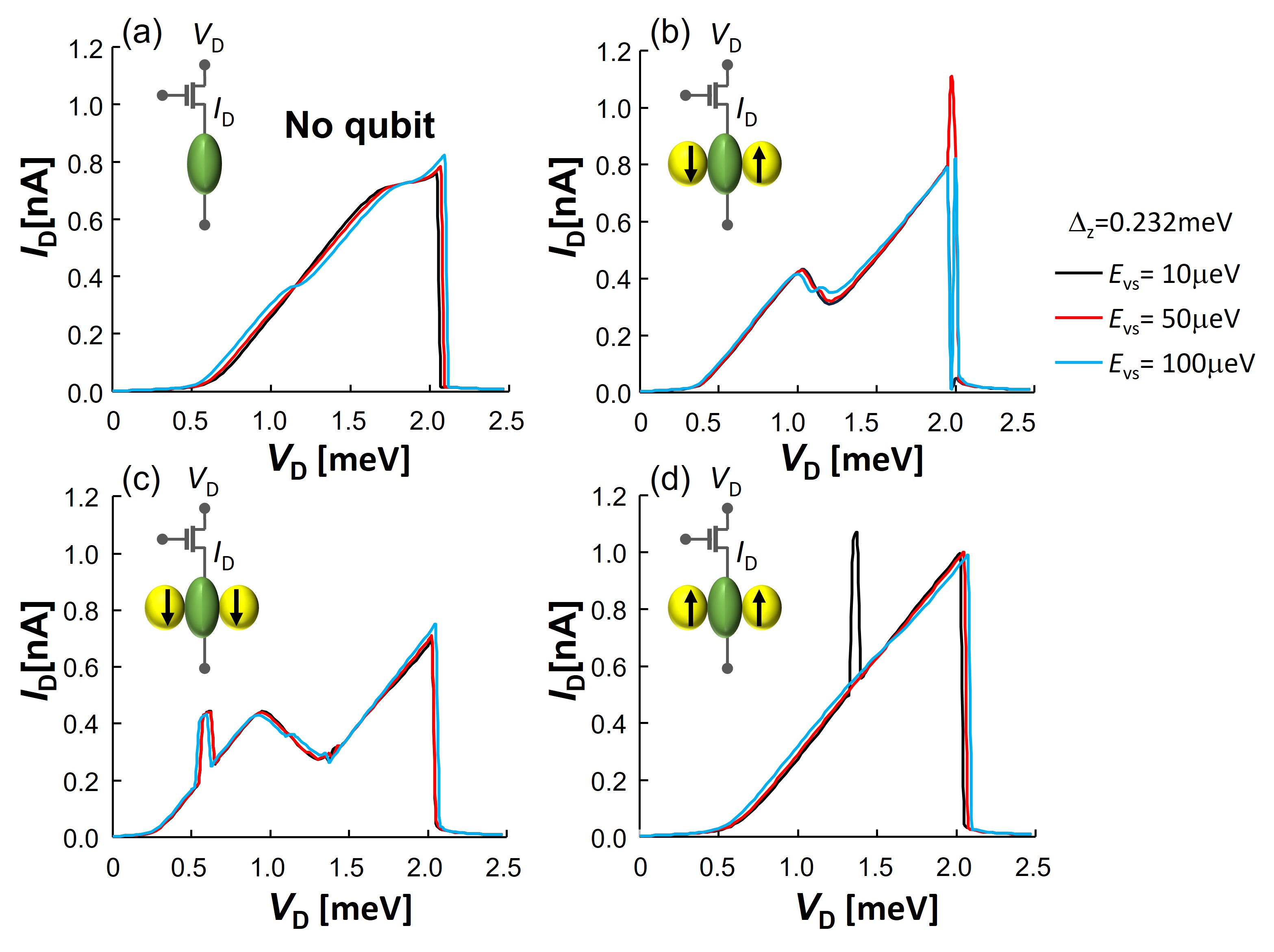
Figure 7 shows IDI_{\rm D}-VDV_{\rm D} with a connection to the transistor when both sides of the qubit-QDs have the same value of EVSE_{\rm VS}. The transistor size L=10L=10 µm is determined to increase the different VoutV_{\rm out} values depending on the qubit states. This situation is realized when the resistance of the transistor is comparable to that of the channel-QD. Because the current characteristics of the transistor have less nonlinearity than those of the channel-QD, the IDI_{\rm D} values of Fig. 7 have gentler slopes than those of Fig. 6(b).

The different IDI_{\rm D}-VDV_{\rm D} characteristics are explained similarly to Fig. 5. For the \downarrow\downarrow pair (|00|00\rangle state) of Fig. 7(c), the resonant energy level of the qubit-QDs, which is the upper energy level of the singlet state, becomes high, as shown in Figs. 3(a) and 3(c), resulting in a peak structure at lower VDV_{\rm D}. Meanwhile, for the \uparrow\uparrow pair (|11|11\rangle state) of Fig. 7(d), the resonant energy level of the qubit-QDs becomes low, as shown in Figs. 3(b) and 3(d). Then, the resonant peak structure is hidden in the original resonant-tunneling peak between the source and drain. The IDI_{\rm D}-VDV_{\rm D} characteristics of Fig. 7(b) takes the middle properties between Figs. 7(c) and 7(d). Due to the presence of two energy levels in each QD, multiple resonant peaks appear in the current characteristics. The sharp peaks observed in Figs. 7(b-d) can be attributed to the complex resonant structure involving six energy levels across the three QDs (as indicated in the denominator of Eq. (LABEL:current_formula)). Consequently, the presence of valley energy levels enhances the transitions between energy levels, resulting in a greater difference in the IDI_{\rm D}s that reflect the qubit states.

IV.5 Nonuniform valley splitting

It has been reported that valley splitting energies vary depending on the location in the range of (100nm)2(100{\rm nm})^{2} Losert . Herein, we consider the case where the three QDs have different valley splitting energies. We calculate EVS=E_{\rm VS}=10, 20, 50, and 100 µeV for QD1(left qubit) and QD3(right qubit). Figure 8 shows the IDI_{\rm D}-VDV_{\rm D} characteristics of the small valley region for W=0.09W=0.09 meV. The shape of the IDI_{\rm D}-VDV_{\rm D} characteristics is primarily determined by E2(0)<E1,E3E_{2}^{(0)}<E_{1},E_{3} (Fig. 8(a)) or E2(0)>E1,E3E_{2}^{(0)}>E_{1},E_{3} (Fig. 8(b)). Because the energy level of QD2 increases as VDV_{\rm D} increases, such as E2=E2(0)+VD/2E_{2}=E_{2}^{(0)}+V_{\rm D}/2, the case of E2(0)<E1,E3E_{2}^{(0)}<E_{1},E_{3} (Fig. 8(a)) shows clear peak structures as a result of energy crossing between E2E_{2} and E1E_{1}, E3E_{3}. Meanwhile, for the case of E2(0)>E1,E3E_{2}^{(0)}>E_{1},E_{3}, nonlinear characteristics appear as a result of higher-order tunneling, resulting in a vague peak structure in Fig. 8(b). By the nonuniformity of the valley splitting, IDI_{\rm D}-VDV_{\rm D} characteristics in Fig. 8 are modified in a more complicated way from those in Fig. 7.

Figure 9 shows the output voltage VoutV_{\rm out} corresponding to Figs. 8(a) and 8(b). For the case of E2(0)<E1,E3E_{2}^{(0)}<E_{1},E_{3} (Fig. 9(a)), a clear separation among various VoutV_{\rm out} values can be observed. In contrast, for the case of E2(0)>E1,E3E_{2}^{(0)}>E_{1},E_{3} (Fig. 9(b)), the difference among VoutV_{\rm out} values becomes small. A larger voltage difference is desirable for distinguishing different qubit states, which is conducted by connected circuits, as in a previous study tanaAPL . Thus, the case of E2(0)<E1,E3E_{2}^{(0)}<E_{1},E_{3} is better for the detection of qubit states.

IV.6 Measurement time

Figure 10 shows the results for tdec/tmeast_{\rm dec}/t_{\rm meas}. Regarding tdec/tmeast_{\rm dec}/t_{\rm meas}, simultaneous peaks of tdec/tmeas>100t_{\rm dec}/t_{\rm meas}>100 appear around the right end of the resonant peak for the case of E2(0)<E1,E3E_{2}^{(0)}<E_{1},E_{3}. In contrast, for the case of E2(0)>E1,E3E_{2}^{(0)}>E_{1},E_{3}, a large tdec/tmeast_{\rm dec}/t_{\rm meas} can be seen around VD=0V_{\rm D}=0, where the energy levels of the three QDs are close to each other. The region of tdec/tmeas>100t_{\rm dec}/t_{\rm meas}>100 for W=0.18W=0.18 meV appears to be smaller than that for W=0.09W=0.09 meV (figure not shown). Increased mixing of resonant energy levels appears to increase the nonlinearity of IDI_{\rm D}-VDV_{\rm D} and increase tdec/tmeast_{\rm dec}/t_{\rm meas}. The valley splitting energy is closer to W=0.09W=0.09 meV than W=0.18W=0.18 meV, and increased energy level mixing is expected at W=0.09W=0.09 meV. Note that tdec/tmeast_{\rm dec}/t_{\rm meas} in Fig. 10 is larger than that in Fig. 18 of appendix C, which is equivalent to no valley splitting case. Therefore, the increased nonlinearity of the current improves the readout in this small nonuniformity of the valley energy levels.

We also calculate EVS1=10E_{\rm VS1}=10 µeV, EVS2=50E_{\rm VS2}=50 µeV, EVS3=100E_{\rm VS3}=100 µeV, and EVS1=10E_{\rm VS1}=10 µeV, EVS2=50E_{\rm VS2}=50 µeV, EVS3=10E_{\rm VS3}=10 µeV, both for E2(0)<E1,E3E_{2}^{(0)}<E_{1},E_{3}. In the former case, we can see the simultaneous peaks tdec/tmeas>100t_{\rm dec}/t_{\rm meas}>100 around the right end of the resonant peak around VD2.0VV_{\rm D}\approx 2.0V (figures not shown). However, in the latter case, the peaks tdec/tmeas>100t_{\rm dec}/t_{\rm meas}>100 around VD2.0VV_{\rm D}\approx 2.0V deviate from each other (figures not shown). Therefore, although it is difficult to obtain a unified understanding of these cases, simultaneous peaks with tdec/tmeas>100t_{\rm dec}/t_{\rm meas}>100 are expected when the valley splitting energies between the nearest QDs are close to each other.

Refer to caption
Figure 8: IDI_{\rm D}-VDV_{\rm D} characteristics in the small valley region (EVS<ΔzE_{\rm VS}<\Delta_{z}). Γ0=3.0×10⁶\Gamma_{0}=3.0\times 10^{-6} eV, EFE_{F}=1 meV, and T=100T=100 mK. L=10L=10 µm, VG=V_{\rm G}=0.1 V, and W=0.09W=0.09 meV. EVS1=10E_{\rm VS1}=10 µeV, EVS2=20E_{\rm VS2}=20 µeV, and EVS3=50E_{\rm VS3}=50 µeV. (a) E1=1.2E_{1}=1.2 meV, E2(0)=0.88E_{2}^{(0)}=0.88 meV, and E3=1.4E_{3}=1.4 meV. (b) E1=1.2E_{1}=1.2 meV, E2(0)=1.4E_{2}^{(0)}=1.4 meV, and E3=1.1E_{3}=1.1 meV.
Refer to caption
Figure 9: VoutV_{\rm out} as a function of VDV_{\rm D} in the small valley region. (a) E1=1.2E_{1}=1.2 meV, E2(0)=0.88E_{2}^{(0)}=0.88 meV, and E3=1.4E_{3}=1.4 meV. (b) E1=1.2E_{1}=1.2 meV, E2(0)=1.4E_{2}^{(0)}=1.4 meV, and E3=1.1E_{3}=1.1 meV. The other parameters are the same as those in Fig. 8.
Refer to caption
Figure 10: tdec/tmeast_{\rm dec}/t_{\rm meas} as a function of VDV_{\rm D} in the small valley region. (a) E1=1.2E_{1}=1.2 meV, E2(0)=0.88E_{2}^{(0)}=0.88 meV, and E3=1.4E_{3}=1.4 meV. (b) E1=1.2E_{1}=1.2 meV, E2(0)=1.4E_{2}^{(0)}=1.4 meV, and E3=1.1E_{3}=1.1 meV. The other parameters are the same as those in Fig. 8. The dotted horizontal line indicates that more than 100 readouts are possible during tdec=100t_{\rm dec}=100 ns above this line. The lower solid line indicates that more than 100 readouts are possible during tdec=1t_{\rm dec}=1 µs above this line.

V Discussions

In this study, we focused on the relationship between the coherence time tdect_{\rm dec} and the measurement time tmeast_{\rm meas} and did not mention how to determine |0|0\rangle and |1|1\rangle in the succeeding circuit, which is connected to the transistor in Fig. 1. Thus, the ratio tdec/tdect_{\rm dec}/t_{\rm dec} does not exactly represent the required number of readouts. In most cases, the qubit state could be determined by taking an average of repeated measurements. If the transistor in Fig. 1 is connected to the sense amplifier such as those in a previous study tanaAPL , a single-shot readout would be possible. For example, tdec/tmeas100t_{\rm dec}/t_{\rm meas}\approx 100 with tdec=100t_{\rm dec}=100 ns means tmeas1t_{\rm meas}\approx 1 ns. Because the switching speed of a conventional CMOS is in the order of ps Jena , the resolution of the output signal by CMOS is higher than the changing time of qubit states, and we can detect the change in the VoutV_{\rm out} using the CMOS circuits. Further analysis regarding the effect of noise by transistors is the future issue.

The electron that enters into the qubit-QD forms a singlet state with the electron in the qubit. If there is no energy relaxation, the electron with the same spin as that when it enters the qubit-QD goes out to the channel-QD because of energy conservation. However, when there is a relaxation process, the qubit state changes. In this study, this process was represented by the static decoherence time of tdect_{\rm dec}. The dynamic description of this process is beyond the scope of this study and is a problem for future studies.

The numerical results of the large valley splitting with the nonuniformity in energy levels are presented in the appendix C. tdec/tmeast_{\rm dec}/t_{\rm meas} becomes smaller with the existence of nonuniformity. This indicates that the nonuniform energy levels degrade the performance of the readout process. However, because of the nonlinear effects of the multiple energy levels, the reduction in tdec/tmeast_{\rm dec}/t_{\rm meas} by the valley splitting seems to be small as long as the nonuniformity is small. The current characteristics under the nonuniformity strongly depend on the system parameters (e.g., EVSE_{\rm VS}, WijW_{ij}, EiE_{i}, and Γi\Gamma_{i}). Thus, the maximum tolerance to the nonuniformity should be determined depending on each system. Hence, systematic estimation is also an issue for future research.

VI Conclusions

In summary, we theoretically investigated the effect of valley splitting on the readout process of spin qubits constructed in a three-QD system, aiming at future two-dimensional qubit arrays. The current formula (Eq.(LABEL:current_formula)) was derived on the basis of the nonequilibrium Green function method by including the mixing of the energy levels in the QDs. In the small valley splitting region (EVS<ΔzE_{\rm VS}<\Delta_{z}) and large valley splitting region (EVS>ΔzE_{\rm VS}>\Delta_{z}), we found the parameter region where more than a hundred readouts are expected (tdec/tmeas>100t_{\rm dec}/t_{\rm meas}>100). In particular, increased mixing of the resonant energy levels enhances the nonlinearity of the current IDI_{\rm D} and improves the readout in the small valley region (larger tdec/tmeast_{\rm dec}/t_{\rm meas}). The degree of mixing is highly dependent on the device parameters, so the optimal values must be determined for each device. These results demonstrate that the proposed system can effectively detect the resonant energy levels of the coupled QD system. Therefore, while a larger valley splitting energy is desirable for qubit operations, the readout of spin states can still be effectively accomplished, even in regions with valley splitting.

DATA AVAILABILITY

The data supporting the findings of this study are available in this article.

Acknowledgements.
We are grateful to T. Mori, H. Fuketa, and S. Takagi for their insightful discussions. This study was partially supported by the MEXT Quantum Leap Flagship Program (MEXT Q-LEAP), Grant Number JPMXS0118069228, Japan. Furthermore, this study was supported by JSPS KAKENHI Grant Number JP22K03497.

AUTHOR CONTRIBUTIONS

T.T. conceived and designed the theoretical calculations. K.O. discussed the results from the experimentalist viewpoint.

CONFLICT OF INTEREST

The authors have no conflicts of interest to disclose.

Appendix A Qubit array aiming at a 3D stacked qubit system

Surface code is a critical area of focus for qubit systems, requiring an error rate of less than 1% Fowler . Various proposals for implementing surface codes using spin qubits have been made Hill ; Veldhorst1 ; Veldhorst ; Li . In Fig. 1(a), it is assumed that independent electrodes are attached to the control gates Vcg,iV_{\text{cg},i} one by one. The wiring for Vcg,iV_{\text{cg},i}s are constructed in parallel to the wiring of the sources and drains.

Our strategy involves leveraging existing commercial transistor architectures to minimize fabrication costs, as advanced transistors can be prohibitively expensive. By stacking the one-dimensional array shown in Fig.1, we can achieve a two-dimensional qubit array suitable for the surface code structure using advanced semiconductor technologies.

Here, we consider the case in which the control gates VcgV_{\text{cg}} in Fig. 1(a) are represented by a single common gate. Two types of stacking structures are shown in Fig. 11. In Fig. 11(a), each qubit-QD is surrounded by four channel-QDs, as proposed in Ref. tanaJAP . In this configuration, each qubit can be controlled by the four channel-QDs, resulting in high controllability. However, the area that the common gate covers over each qubit QD is small, as shown in Fig. 12, meaning that gate controllability will depend on the detailed 3D structure.

In Fig. 11(b), qubits are arranged diagonally, resulting in coupling between diagonally positioned qubits. In this case, the four qubits surrounding each channel QD must have different energy levels to independently control qubit-qubit coupling and individual qubit. On the other hand, the electric potential of the qubits can be effectively controlled because each qubit is surrounded by four directions of influence from the common gate. Currently, the optimal structure for realizing the design in Fig. 1 is a future issue. To further refine our design, we have initiated technical CAD simulations, as detailed in Ref. tanaTCAD .

Refer to caption
Figure 11: Two types of the stacking structures using the qubit array in Fig.1(a). Cross section at the center of QDs. (a) Each qubit is surround by four channel-QDs. (b) Each channel-QD is surrounded by four qubits. The yellow circles represent the qubit-QDs, whereas the green ellipse represents the channel-QDs, which serve as the coupling and readout of the qubits. All QDs are surrounded by insulators such as SiO2. Spin directions are changed using a magnetic field gradient method, utilizing micromagnets placed above the structure (not shown in the figure). The static magnetic field BzB_{z} is applied along the zz-direction.
Refer to caption
Figure 12: Example of the common gate structure in Fig. 11(a). The common gate is connected to the qubit-QD through the gap between the source-drain wires. The source-drain wires are also placed over the qubit-QD. All structures are surrounded by SiO2.
Refer to caption
Figure 13: Simple analysis of the resonant-tunneling phenomena. Two situations are observed depending on the relative energy between the electrode and channel-QD (QD2). (a)E2(0)>EFE_{2}^{(0)}>E_{F}. (b) E2(0)<EFE_{2}^{(0)}<E_{F}. The result is listed in Table 1.

Appendix B Analysis of resonant-tunneling without qubit

B.1 No magnetic field case

In this section, we will analyze the simple resonant peak structure without qubits or a magnetic field. The general trend of the peak current can be understood by examining the simple band structure. Two different cases are considered, based on whether E2(0)<EFE_{2}^{(0)}<E_{F} or E2(0)>EFE_{2}^{(0)}>E_{F}, as shown in Fig. 13. When the resonant current begins to flow, the energy level of the source surpasses that of the channel-QD (QD2). This can be represented as follows:

EF+VD>E2(0)+VD/2.E_{F}+V_{\rm D}>E_{2}^{(0)}+V_{\rm D}/2. (19)

Moreover, the energy of the channel-QD should exceed the drain energy level, resulting in:

E2(0)+VD/2>EF.E_{2}^{(0)}+V_{\rm D}/2>E_{F}. (20)

These result in the following:

VD>2|EFE2(0)|.V_{\rm D}>2|E_{F}-E_{2}^{(0)}|. (21)

The resonant peak disappears when E2(0)+VD/2E_{2}^{(0)}+V_{\rm D}/2 is less than that at the bottom of the source energy level(right side of Fig. 13(a)), which is expressed as follows:

E2(0)+VD/2<VD.E_{2}^{(0)}+V_{\rm D}/2<V_{\rm D}. (22)

Therefore, the bias voltage VDoffV_{\rm D}^{\rm off} representing the disappearance of the resonant peak is expressed as follows:

VDoff=2E2(0).V_{\rm D}^{\rm off}=2E_{2}^{(0)}. (23)

Thus, for E2(0)<EFE_{2}^{(0)}<E_{F}(Fig. 13(a)), the resonant peak region is approximately expressed as follows:

2(EFE2(0))<VD<2E2(0),2(E_{F}-E_{2}^{(0)})<V_{\rm D}<2E_{2}^{(0)}, (24)

where VDonV_{\rm D}^{\rm on} is expressed as follows:

VDon=2(EFE2(0)).V_{\rm D}^{\rm on}=2(E_{F}-E_{2}^{(0)}). (25)

The approximate values of the width and center of the resonant peak are 4E2(0)2EF4E_{2}^{(0)}-2E_{F} and EFE_{F}, respectively.

For E2(0)>EFE_{2}^{(0)}>E_{F} (Fig. 13(b)), we have

2(E2(0)EF)<VD<2E2(0).2(E_{2}^{(0)}-E_{F})<V_{\rm D}<2E_{2}^{(0)}. (26)

where VDonV_{\rm D}^{\rm on} is expressed as follows:

VDon=2(E2(0)EF).V_{\rm D}^{\rm on}=2(E_{2}^{(0)}-E_{F}). (27)

The approximate values of the width and center of the resonant peak are EFE_{F} and 4E2(0)2EF4E_{2}^{(0)}-2E_{F}, respectively. The results are listed in Table I.

Table 1: Analysis of resonant-tunneling structure without magnetic field.
Situations Peak region Peak width Peak center
E2(0)<EFE_{2}^{(0)}\!<\!E_{F} 2(EFE2(0))<VD<2E2(0)2(E_{F}\!-\!E_{2}^{(0)})\!<\!V_{\rm D}\!<\!2E_{2}^{(0)} 4E2(0)2EF4E_{2}^{(0)}\!\!-\!2E_{F} EFE_{F}
E2(0)>EFE_{2}^{(0)}\!>\!E_{F} 2(E2(0)EF)<VD<2E2(0)2(E_{2}^{(0)}\!\!-\!E_{F})\!<\!V_{\rm D}\!<\!2E_{2}^{(0)} 2EF2E_{F} 2E2(0)EF2E_{2}^{(0)}\!\!-\!E_{F}

B.2 Finite magnetic field case

When a magnetic field is present, the \uparrow and \downarrow spin currents can be analyzed by adjusting the Fermi energy to EFΔz/2E_{F}\mp\Delta_{z}/2, as discussed in the main text. Here, we will focus on the \uparrow-current case (the \downarrow-current case can be addressed by substituting Δz\Delta_{z} by Δz-\Delta_{z}). The resonant-tunneling \uparrow-current can be approximated as outlined in Table 2, where EFE_{F} in Table 1 is replaced by EFΔz/2E_{F}-\Delta_{z}/2. For example, when E2(0)+Δz/2<EFE_{2}^{(0)}+\Delta_{z}/2<E_{F} is satisfied, the bias voltage at which the resonant peak appears is expressed as follows:

VDon=2(EFE2(0)Δz/2).V_{\rm D\uparrow}^{\rm on}=2(E_{F}-E_{2}^{(0)}-\Delta_{z}/2). (28)

The end of the resonant peak is expressed as follows:

VDoff=2E2(0).V_{{\rm D}\uparrow}^{\rm off}=2E_{2}^{(0)}. (29)

Correspondingly, the resonant peak region is expressed as:

2(EFE2(0)Δz/2)<VD<2E2(0).2(E_{F}-E_{2}^{(0)}-\Delta_{z}/2)<V_{\rm D}<2E_{2}^{(0)}. (30)

The width and center of the resonant peak are approximated as 4E2(0)2EF+Δz4E_{2}^{(0)}-2E_{F}+\Delta_{z} and EFΔz/2E_{F}-\Delta_{z}/2, respectively.

Table 2: Analysis of the resonant-tunneling structure of the \uparrow-current with magnetic field. The results of the \downarrow-current are obtained by replacing Δz\Delta_{z} by Δz-\Delta_{z}.
Situations Peak region Peak width Peak center
E2(0)+Δz/2<EFE_{2}^{(0)}+\Delta_{z}/2\!<\!E_{F} 2(EFE2(0)Δz/2)<VD<2E2(0)2(E_{F}\!-\!E_{2}^{(0)}\!-\Delta_{z}/2)\!<\!V_{\rm D}\!<\!2E_{2}^{(0)} 4E2(0)+Δz2EF4E_{2}^{(0)}\!\!+\Delta_{z}-\!2E_{F} EFΔz/2E_{F}-\Delta_{z}/2
E2(0)+Δz/2>EFE_{2}^{(0)}+\Delta_{z}/2\!>\!E_{F} 2(E2(0)+Δz/2EF)<VD<2E2(0)2(E_{2}^{(0)}+\Delta_{z}/2\!\!-\!E_{F})\!<\!V_{\rm D}\!<\!2E_{2}^{(0)} 2EFΔz2E_{F}-\Delta_{z} 2E2(0)+Δz/2EF2E_{2}^{(0)}\!\!+\Delta_{z}/2-\!E_{F}

Appendix C Nonuniform large valley region

In this section, we explore the region of nonuniform large valley splitting (E1E3E_{1}\neq E_{3} and EVS>ΔzE_{\rm VS}>\Delta_{z}). Owing to valley splitting, the energy diagram of qubit-QDs changes from Fig. 14(a) to Fig. 14(b). Consequently, in cases of large valley splitting, the tunneling restrictions remain unchanged compared with no valley splitting case (Fig. 15).

The IDI_{\rm D}-VDV_{\rm D}, VoutV_{\rm out}, and tdec/tmeast_{\rm dec}/t_{\rm meas} of the EVS>ΔzE_{\rm VS}>\Delta_{z} and EVS>VDE_{\rm VS}>V_{\rm D} are shown in Figs. 16-18. The difference between Figs. 16 (a) and (b) lies in the condition of E2(0)<E1,E3E_{2}^{(0)}<E_{1},E_{3} (Fig. 16(a)) and E2(0)>E1,E3E_{2}^{(0)}>E_{1},E_{3} (Fig. 16(b)). As the energy level of QD2 increases with VDV_{\rm D}, as indicated by E2=E2(0)+VD/2E_{2}=E_{2}^{(0)}+V_{\rm D}/2, a clear resonant peak is observed for E2(0)<E1,E3E_{2}^{(0)}<E_{1},E_{3} (Fig. 16(a)). The resonant peak structure is influenced by the spin states of QD1 and QD3. Therefore, depending on the qubit state (Fig. 15), different IDI_{\rm D}s are obtained. This difference in current results in different measurement times. For E2(0)>E1,E3E_{2}^{(0)}>E_{1},E_{3}(Fig.16(b)), the variation in IDI_{\rm D}VDV_{\rm D} characteristics among different qubit states is not pronounced as when E2(0)<E1,E3E_{2}^{(0)}<E_{1},E_{3}(Fig.16(a)). However, upon comparing Fig.16(b) with Fig.8(b), the differences in IDI_{\rm D}-VDV_{\rm D} characteristics increases slightly for the large valleys.

The VoutV_{\rm out} for a gate length L=10μL=10~{}\mum of the transistor is shown in Fig. 17. Notably, E2(0)<E1,E3E_{2}^{(0)}<E_{1},E_{3} (Fig. 17(a)) is superior to E2(0)>E1,E3E_{2}^{(0)}>E_{1},E_{3} (Fig. 17(b)) for the detection.

Figure 18 shows the results for tdec/tmeast_{\rm dec}/t_{\rm meas} for the nonuniform large valley splittings. Above the blue dotted line, tdec/tmeast_{\rm dec}/t_{\rm meas} exceeds 100 for tdec=100t_{\rm dec}=100 ns. Above the solid horizontal line, tdec/tmeast_{\rm dec}/t_{\rm meas} exceeds 100 for tdec=1μt_{\rm dec}=1\mus. For the uniform valley splitting energies (E1=E3=1.2E_{1}=E_{3}=1.2 meV and E2(0)=1.1E_{2}^{(0)}=1.1 meV), the region of tdec/tmeas>100t_{\rm dec}/t_{\rm meas}>100 for tdec=100t_{\rm dec}=100 ns to all qubit states is found near VD2.3V_{\rm D}\approx 2.3 meV (figures not shown). However, in Fig. 18, there is no region where tdec/tmeas>100t_{\rm dec}/t_{\rm meas}>100 for tdec=100t_{\rm dec}=100 ns is satisfied for all qubit states. Therefore, the nonuniform energy levels degrade the tdec/tmeast_{\rm dec}/t_{\rm meas}. If we can increase the coherence time to tdec=1μt_{\rm dec}=1\mus, we can find the region of tdec/tmeas>100t_{\rm dec}/t_{\rm meas}>100 for all qubit states in Figs. 18(a) and (b).

Refer to caption
Figure 14: Energy band diagram of the two qubit states (|0|0\rangle or |1|1\rangle). (a) No valley splitting case. (b) Large valley case. The solid arrows denote the spins of the qubits (first electron). The arrows with white circles represent the possible spin state in which the second electron enters the QDs. In the large valley region, the tunneling possibilities are similar to those of the no valley splitting case.
Refer to caption
Figure 15: Tunneling profile between the channel-QD(QD2) and qubit-QD for large valley splitting. The tunneling possibilities are the same as those in small valley splitting (Fig. 3). Here, the qubit-QD represents both QD1 and QD3. (a) and (b) represent the \uparrow-current. (c) and (d) represent \downarrow-current. From (a) and (b), \uparrow-current can exchange \uparrow-spin electron only when the qubit state is |0|0\rangle. From (c) and (d), \downarrow-current can exchange \downarrow-spin electron only when the qubit state is |1|1\rangle.
Refer to caption
Figure 16: IDI_{\rm D}-VDV_{\rm D} characteristics in the small valley region. Γ0=3.0×10⁶\Gamma_{0}=3.0\times 10^{-6} eV, EFE_{F}=1 meV, T=100T=100mK. L=10μL=10\mu m, W=0.18W=0.18 meV, and VG=V_{G}=0.1 V. (a) E1=1.2E_{1}=1.2 meV, E2(0)=1.1E_{2}^{(0)}=1.1 meV, and E3=1.4E_{3}=1.4 meV. (b) E1=1.2E_{1}=1.2 meV, E2(0)=1.4E_{2}^{(0)}=1.4 meV, and E3=1.1E_{3}=1.1meV.
Refer to caption
Figure 17: VoutV_{\rm out} as a function of VDV_{\rm D} in the large valley region. (a) E1=1.2E_{1}=1.2 meV, E2(0)=1.1E_{2}^{(0)}=1.1 meV, and E3=1.4E_{3}=1.4 meV. (b) E1=1.2E_{1}=1.2 meV, E2(0)=1.4E_{2}^{(0)}=1.4 meV, and E3=1.1E_{3}=1.1 meV. Other parameters align with those in Fig. 16.
Refer to caption
Figure 18: tdec/tmeast_{\rm dec}/t_{\rm meas} as a function of VDV_{\rm D} in the large valley region. (a) E1=1.2E_{1}=1.2 meV, E2(0)=1.1E_{2}^{(0)}=1.1 meV, and E3=1.4E_{3}=1.4 meV. (b) E1=1.2E_{1}=1.2 meV, E2(0)=1.4E_{2}^{(0)}=1.4 meV, and E3=1.1E_{3}=1.1 meV. Other parameters align with those in Fig. 16. The dotted horizontal line indicates that more than 100 readouts are possible during the tdec=100t_{\rm dec}=100 ns above this line. The lower solid line indicates that over 100 readouts are possible during the tdec=1μt_{\rm dec}=1\mus above this line.

Appendix D Derivation of Green functions

The equation of motion method can be utilized to derive various Green functions. In the following theoretical approach using nonequilibrium Green functions, the electrodes are referred to as the left and right electrodes, denoted as LL and RR instead of SS and DD, respectively.

The equation for the operator d1a(ω)d_{1a}(\omega) is given by

ωd1a(ω)=[d1a(ω),H]\displaystyle\omega d_{1a}(\omega)=[d_{1a}(\omega),H] (31)
=\displaystyle= E1ad1a+W12aad2a+W12abd2b.\displaystyle E_{1a}d_{1a}+W_{12aa}d_{2a}+W_{12ab}d_{2b}.

Similarly, we have

(ωE1b)d1b\displaystyle(\omega-E_{1b})d_{1b} =\displaystyle= W12bbd2b+W12bad2a,\displaystyle W_{12bb}d_{2b}+W_{12ba}d_{2a},
(ωE3a)d3a\displaystyle(\omega-E_{3a})d_{3a} =\displaystyle= W32aad2a+W32abd2b,\displaystyle W_{32aa}d_{2a}+W_{32ab}d_{2b},
(ωE3b)d3b\displaystyle(\omega-E_{3b})d_{3b} =\displaystyle= W32bbd2b+W32bad2a,\displaystyle W_{32bb}d_{2b}+W_{32ba}d_{2a},
(ωE2a)d2a\displaystyle(\omega-E_{2a})d_{2a} =\displaystyle= α=L,RkαVkαsfkαs+W12aad1a+W12bad1b\displaystyle\!\sum_{\alpha=L,R}\sum_{k_{\alpha}}V_{k_{\alpha}s}^{*}f_{k_{\alpha}s}+W_{12aa}^{*}d_{1a}+W_{12ba}^{*}d_{1b}
+W32aad3a+W32bad3b,\displaystyle+W_{32aa}^{*}d_{3a}+W_{32ba}^{*}d_{3b},
(ωEkα)fkα\displaystyle(\omega-E_{k_{\alpha}})f_{k_{\alpha}} =\displaystyle= Vkα,ad2a+Vkα,bd2b,\displaystyle V_{k_{\alpha},a}d_{2a}+V_{k_{\alpha},b}d_{2b},

From Eq.(31),

(ωE1a)d1ad1b=W12aad2ad1b+W12abd2bd1b,(\omega-E_{1a})\langle d_{1a}^{\dagger}d_{1b}\rangle=W_{12aa}^{*}\langle d_{2a}^{\dagger}d_{1b}\rangle+W_{12ab}^{*}\langle d_{2b}^{\dagger}d_{1b}\rangle, (32)

which results in the construction of the conventional time-ordered Green function, expressed as follows:

(ωE1a)Gd1bd1at=W12aaGd1bd2at+W12abGd1bd2bt.(\omega-E_{1a})G_{d_{1b}d_{1a}}^{t}=W_{12aa}^{*}G_{d_{1b}d_{2a}}^{t}+W_{12ab}^{*}G_{d_{1b}d_{2b}}^{t}. (33)

According to Jauho’s procedure Jauho , no interaction is included in the lead, and we have

Gd1bd1at\displaystyle G_{d_{1b}d_{1a}}^{t} =\displaystyle= [W12aaGd1bd2at+W12abGd1bd2bt]Σ1a,\displaystyle\bigl{[}W_{12aa}^{*}G_{d_{1b}d_{2a}}^{t}+W_{12ab}^{*}G_{d_{1b}d_{2b}}^{t}\bigr{]}\Sigma_{1a}, (34)

where Σ1a1/(ωE1a)\Sigma_{1a}\equiv 1/(\omega-E_{1a}). For simplicity, tt is omitted from the shoulder of Gd1bd1atG_{d_{1b}d_{1a}}^{t} in the following. We then obtain the equations of the Green functions as follows:

Gd1bd1a\displaystyle G_{d_{1b}d_{1a}} =\displaystyle= [W12aaGd1bd2a+W12abGd1bd2b]Σ1a,\displaystyle\bigl{[}W_{12aa}^{*}G_{d_{1b}d_{2a}}+W_{12ab}^{*}G_{d_{1b}d_{2b}}\bigr{]}\Sigma_{1a},
Gd1ad1a\displaystyle G_{d_{1a}d_{1a}} =\displaystyle= [W12aaGd1ad2a+W12abGd1ad2b+1]Σ1a,\displaystyle\bigl{[}W_{12aa}^{*}G_{d_{1a}d_{2a}}+W_{12ab}^{*}G_{d_{1a}d_{2b}}+1\bigr{]}\Sigma_{1a},
Gd3ad1a\displaystyle G_{d_{3a}d_{1a}} =\displaystyle= [W12aaGd3ad2a+W12abGd3ad2b]Σ1a,\displaystyle\bigl{[}W_{12aa}^{*}G_{d_{3a}d_{2a}}+W_{12ab}^{*}G_{d_{3a}d_{2b}}\bigr{]}\Sigma_{1a},
Gd3bd1a\displaystyle G_{d_{3b}d_{1a}} =\displaystyle= [W12aaGd3bd2a+W12abGd3bd2b]Σ1a,\displaystyle\bigl{[}W_{12aa}^{*}G_{d_{3b}d_{2a}}+W_{12ab}^{*}G_{d_{3b}d_{2b}}\bigr{]}\Sigma_{1a},
Gd2ad1a\displaystyle G_{d_{2a}d_{1a}} =\displaystyle= [W12aaGd2ad2a+W12abGd2ad2b]Σ1a,\displaystyle\bigl{[}W_{12aa}^{*}G_{d_{2a}d_{2a}}+W_{12ab}^{*}G_{d_{2a}d_{2b}}\bigr{]}\Sigma_{1a}, (35)
Gd2bd1a\displaystyle G_{d_{2b}d_{1a}} =\displaystyle= [W12aaGd2bd2a+W12abGd2bd2b]Σ1a.\displaystyle\bigl{[}W_{12aa}^{*}G_{d_{2b}d_{2a}}+W_{12ab}^{*}G_{d_{2b}d_{2b}}\bigr{]}\Sigma_{1a}. (36)

Regarding the Green function of the electrodes, we obtain

(ωEkαa)fkαVkα,ad2a+Vkα,bd2b.(\omega-E_{k_{\alpha}a})f_{k_{\alpha}}V_{k_{\alpha},a}d_{2a}+V_{k_{\alpha},b}d_{2b}. (37)

Therefore,

(ωEkαa)Gd2afkα=Vkα,aGd2ad2a+Vkα,bGd2ad2b.(\omega-E_{k_{\alpha}a})G_{d_{2a}f_{k_{\alpha}}}=V_{k_{\alpha},a}^{*}G_{d_{2a}d_{2a}}+V_{k_{\alpha},b}^{*}G_{d_{2a}d_{2b}}. (38)

This results in

Gd2afkα\displaystyle G_{d_{2a}f_{k_{\alpha}}} =\displaystyle= [Vkα,aGd2ad2a+Vkα,bGd2ad2b]gkαa,\displaystyle\bigl{[}V_{k_{\alpha},a}^{*}G_{d_{2a}d_{2a}}+V_{k_{\alpha},b}^{*}G_{d_{2a}d_{2b}}\bigr{]}g_{k_{\alpha}a}, (39)
Gd2bfkα\displaystyle G_{d_{2b}f_{k_{\alpha}}} =\displaystyle= [Vkα,aGd2bd2a+Vkα,bGd2bd2b]gkαa,\displaystyle\bigl{[}V_{k_{\alpha},a}^{*}G_{d_{2b}d_{2a}}+V_{k_{\alpha},b}^{*}G_{d_{2b}d_{2b}}\bigr{]}g_{k_{\alpha}a},
Gd1afkα\displaystyle G_{d_{1a}f_{k_{\alpha}}} =\displaystyle= [Vkα,aGd1ad2a+Vkα,bGd1ad2b]gkαa,\displaystyle\bigl{[}V_{k_{\alpha},a}^{*}G_{d_{1a}d_{2a}}+V_{k_{\alpha},b}^{*}G_{d_{1a}d_{2b}}\bigr{]}g_{k_{\alpha}a},
Gd1bfkα\displaystyle G_{d_{1b}f_{k_{\alpha}}} =\displaystyle= [Vkα,aGd1bd2a+Vkα,bGd1bd2b]gkαa,\displaystyle\bigl{[}V_{k_{\alpha},a}^{*}G_{d_{1b}d_{2a}}+V_{k_{\alpha},b}^{*}G_{d_{1b}d_{2b}}\bigr{]}g_{k_{\alpha}a},
Gd3afkα\displaystyle G_{d_{3a}f_{k_{\alpha}}} =\displaystyle= [Vkα,aGd3ad2a+Vkα,bGd3ad2b]gkαa,\displaystyle\bigl{[}V_{k_{\alpha},a}^{*}G_{d_{3a}d_{2a}}+V_{k_{\alpha},b}^{*}G_{d_{3a}d_{2b}}\bigr{]}g_{k_{\alpha}a},
Gd3bfkα\displaystyle G_{d_{3b}f_{k_{\alpha}}} =\displaystyle= [Vkα,aGd3bd2a+Vkα,bGd3bd2b]gkαa,\displaystyle\bigl{[}V_{k_{\alpha},a}^{*}G_{d_{3b}d_{2a}}+V_{k_{\alpha},b}^{*}G_{d_{3b}d_{2b}}\bigr{]}g_{k_{\alpha}a},
Gd1afkα\displaystyle G_{d_{1a}f_{k_{\alpha}}} =\displaystyle= [Vkα,aGd1ad2a+Vkα,bGd1ad2b]gkαa,\displaystyle\bigl{[}V_{k_{\alpha},a}^{*}G_{d_{1a}d_{2a}}+V_{k_{\alpha},b}^{*}G_{d_{1a}d_{2b}}\bigr{]}g_{k_{\alpha}a},
Gfkβfkα\displaystyle G_{f_{k_{\beta}}f_{k_{\alpha}}} =\displaystyle= [Vkα,aGfkβd2a+Vkα,bGfkβd2b+δkα,kβ]gkαa.\displaystyle\bigl{[}V_{k_{\alpha},a}^{*}G_{f_{k_{\beta}}d_{2a}}+V_{k_{\alpha},b}^{*}G_{f_{k_{\beta}}d_{2b}}+\delta_{k_{\alpha},k_{\beta}}\bigr{]}g_{k_{\alpha}a}.

D.1 Equations of the channel-QD Green functions

Regarding the Green functions of the channel-QD, we obtain

(ωE2a)d2a\displaystyle(\omega-E_{2a})d_{2a} =\displaystyle= α=L,RkαVkαafkαa+W12aad1a+W12bad1b\displaystyle\!\sum_{\alpha=L,R}\sum_{k_{\alpha}}V_{k_{\alpha}a}^{*}f_{k_{\alpha}a}+W_{12aa}^{*}d_{1a}+W_{12ba}^{*}d_{1b}
+W32aad3a+W32bad3b.\displaystyle+W_{32aa}^{*}d_{3a}+W_{32ba}^{*}d_{3b}.

Therefore,

Gd1ad2a=[α=L,RkαVkα,aGd1afkα+W12aaGd1ad1a\displaystyle G_{d_{1a}d_{2a}}=\bigl{[}\!\sum_{\alpha=L,R}\sum_{k_{\alpha}}V_{k_{\alpha},a}G_{d_{1a}f_{k_{\alpha}}}+W_{12aa}G_{d_{1a}d_{1a}}
+W12baGd1ad1b+W32aaGd1ad3a+W32baGd1ad3b]Σ2a,\displaystyle+W_{12ba}G_{d_{1a}d_{1b}}+W_{32aa}G_{d_{1a}d_{3a}}+W_{32ba}G_{d_{1a}d_{3b}}\bigr{]}\Sigma_{2a},
Gd1bd2a=[α=L,RkαVkα,aGd1bfkα+W12aaGd1bd1a\displaystyle G_{d_{1b}d_{2a}}=\!\bigl{[}\sum_{\alpha=L,R}\sum_{k_{\alpha}}V_{k_{\alpha},a}G_{d_{1b}f_{k_{\alpha}}}+W_{12aa}G_{d_{1b}d_{1a}}
+W12baGd1bd1b+W32aaGd1bd3a+W32baGd1bd3b]Σ2a,\displaystyle+W_{12ba}G_{d_{1b}d_{1b}}+W_{32aa}G_{d_{1b}d_{3a}}+W_{32ba}G_{d_{1b}d_{3b}}\bigr{]}\Sigma_{2a},
Gd3ad2a=[α=L,RkαVkα,aGd3afkα+W12aaGd3ad1a\displaystyle G_{d_{3a}d_{2a}}=\!\bigl{[}\sum_{\alpha=L,R}\sum_{k_{\alpha}}V_{k_{\alpha},a}G_{d_{3a}f_{k_{\alpha}}}+W_{12aa}G_{d_{3a}d_{1a}}
+W12baGd3ad1b+W32aaGd3ad3a+W32baGd3ad3b]Σ2a,\displaystyle+W_{12ba}G_{d_{3a}d_{1b}}+W_{32aa}G_{d_{3a}d_{3a}}+W_{32ba}G_{d_{3a}d_{3b}}\bigr{]}\Sigma_{2a},
Gd3bd2a=[α=L,RkαVkα,aGd3bfkα+W12aaGd3bd1a\displaystyle G_{d_{3b}d_{2a}}=\!\bigl{[}\sum_{\alpha=L,R}\sum_{k_{\alpha}}V_{k_{\alpha},a}G_{d_{3b}f_{k_{\alpha}}}+W_{12aa}G_{d_{3b}d_{1a}}
+W12baGd3bd1b+W32aaGd3bd3a+W32baGd3bd3b]Σ2a,\displaystyle+W_{12ba}G_{d_{3b}d_{1b}}+W_{32aa}G_{d_{3b}d_{3a}}+W_{32ba}G_{d_{3b}d_{3b}}\bigr{]}\Sigma_{2a},
Gd2ad2a=[α=L,RkαVkα,aGd2afkα+W12aaGd2ad1a\displaystyle G_{d_{2a}d_{2a}}\!=\!\bigl{[}\sum_{\alpha=L,R}\sum_{k_{\alpha}}\!V_{k_{\alpha},a}G_{d_{2a}f_{k_{\alpha}}}\!+W_{12aa}G_{d_{2a}d_{1a}}
+W12baGd2ad1b+W32aaGd2ad3a+W32baGd2ad3b+1]Σ2a,\displaystyle\!+W_{12ba}G_{d_{2a}d_{1b}}\!+W_{32aa}G_{d_{2a}d_{3a}}\!+\!W_{32ba}G_{d_{2a}d_{3b}}\!+\!1\bigr{]}\Sigma_{2a},
Gd2bd2a=[α=L,RkαVkα,aGd2bfkαΣ2a+W12aaGd2bd1a\displaystyle G_{d_{2b}d_{2a}}=\!\bigl{[}\sum_{\alpha=L,R}\sum_{k_{\alpha}}V_{k_{\alpha},a}G_{d_{2b}f_{k_{\alpha}}}\Sigma_{2a}+W_{12aa}G_{d_{2b}d_{1a}}
+W12baGd2bd1b+W32aaGd2bd3a+W32baGd2bd3b]Σ2a,\displaystyle+W_{12ba}G_{d_{2b}d_{1b}}+W_{32aa}G_{d_{2b}d_{3a}}+W_{32ba}G_{d_{2b}d_{3b}}\bigr{]}\Sigma_{2a},
Gfkβd2a=[α=L,RkαVkα,aGfkβfkα+W12aaGfkβd1a\displaystyle G_{f_{k_{\beta}}d_{2a}}=\!\bigl{[}\sum_{\alpha=L,R}\sum_{k_{\alpha}}V_{k_{\alpha},a}G_{f_{k_{\beta}}f_{k_{\alpha}}}+W_{12aa}G_{f_{k_{\beta}}d_{1a}}
+W12baGfkβd1b+W32aaGfkβd3a+W32baGfkβd3b]Σ2a.\displaystyle+W_{12ba}G_{f_{k_{\beta}}d_{1b}}+W_{32aa}G_{f_{k_{\beta}}d_{3a}}+W_{32ba}G_{f_{k_{\beta}}d_{3b}}\bigr{]}\Sigma_{2a}.

Using Eqs.(35), and (36) with other Green functions, Eq.(D.1) is transformed to:

Gd2ad2a=[α=L,RkαVkα,aGd2afkα+W12aaGd2ad1a\displaystyle G_{d_{2a}d_{2a}}\!=\bigl{[}\!\!\sum_{\alpha=L,R}\sum_{k_{\alpha}}V_{k_{\alpha},a}G_{d_{2a}f_{k_{\alpha}}}\!+\!W_{12aa}G_{d_{2a}d_{1a}} (42)
+\displaystyle+ W12baGd2ad1b+W32aaGd2ad3a+W32baGd2ad3b+1]Σ2a\displaystyle\!W_{12ba}G_{d_{2a}d_{1b}}\!+\!W_{32aa}G_{d_{2a}d_{3a}}\!+\!W_{32ba}G_{d_{2a}d_{3b}}\!+\!1\bigr{]}\Sigma_{2a}
=\displaystyle= α=L,RkαVkα,a(Vkα,aGd2ad2a+Vkα,bGd2ad2b)gkαaΣ2a\displaystyle\sum_{\alpha=L,R}\sum_{k_{\alpha}}V_{k_{\alpha},a}(V_{k_{\alpha},a}^{*}G_{d_{2a}d_{2a}}+V_{k_{\alpha},b}^{*}G_{d_{2a}d_{2b}})g_{k_{\alpha}a}\Sigma_{2a}
+\displaystyle+ W12aa(W12aaGd2ad2a+W12abGd2ad2b)Σ1aΣ2a\displaystyle W_{12aa}(W_{12aa}^{*}G_{d_{2a}d_{2a}}+W_{12ab}^{*}G_{d_{2a}d_{2b}})\Sigma_{1a}\Sigma_{2a}
+\displaystyle+ W12ba(W12bbGd2ad2b+W12baGd2ad2a)Σ1bΣ2a\displaystyle W_{12ba}(W_{12bb}^{*}G_{d_{2a}d_{2b}}+W_{12ba}^{*}G_{d_{2a}d_{2a}})\Sigma_{1b}\Sigma_{2a}
+\displaystyle+ W32aa(W32aaGd2ad2a+W32abGd2ad2b)Σ3aΣ2a\displaystyle W_{32aa}(W_{32aa}^{*}G_{d_{2a}d_{2a}}+W_{32ab}^{*}G_{d_{2a}d_{2b}})\Sigma_{3a}\Sigma_{2a}
+\displaystyle+ W32ba(W32bbGd2ad2b+W32baGd2ad2a)Σ3bΣ2a+Σ2a\displaystyle W_{32ba}(W_{32bb}^{*}G_{d_{2a}d_{2b}}+W_{32ba}^{*}G_{d_{2a}d_{2a}})\Sigma_{3b}\Sigma_{2a}\!+\!\Sigma_{2a}
=\displaystyle= (Gd2ad2a+Gd2ad2b)ΣfaΣ2a\displaystyle(G_{d_{2a}d_{2a}}+G_{d_{2a}d_{2b}})\Sigma_{fa}\Sigma_{2a}
+\displaystyle+ Gd2ad2aAvaa+Gd2ad2bAvab+Σ2a.\displaystyle G_{d_{2a}d_{2a}}A_{vaa}+G_{d_{2a}d_{2b}}A_{vab}\!+\!\Sigma_{2a}.

Therefore, we have

Gd2ad2a[1ΣfaΣ2aAvaa]=Gd2ad2b[ΣfaΣ2a+Avab]+Σ2a.\displaystyle G_{d_{2a}d_{2a}}\![1-\Sigma_{fa}\Sigma_{2a}-A_{vaa}]=G_{d_{2a}d_{2b}}[\Sigma_{fa}\Sigma_{2a}+A_{vab}]\!+\!\Sigma_{2a}.
(43)

Here, we define

Avaa\displaystyle A_{vaa} \displaystyle\equiv (|W12aa|2Σ1a+|W12ba|2Σ1b+|W32aa|2Σ3a\displaystyle(|W_{12aa}|^{2}\Sigma_{1a}+|W_{12ba}|^{2}\Sigma_{1b}+|W_{32aa}|^{2}\Sigma_{3a}
+|W32ba|2Σ3b)Σ2a,\displaystyle+|W_{32ba}|^{2}\Sigma_{3b})\Sigma_{2a},
Avbb\displaystyle A_{vbb} \displaystyle\equiv (|W12bb|2Σ1b+|W12ab|2Σ1a+|W32bb|2Σ3b\displaystyle(|W_{12bb}|^{2}\Sigma_{1b}+|W_{12ab}|^{2}\Sigma_{1a}+|W_{32bb}|^{2}\Sigma_{3b}
+|W32ab|2Σ3a)Σ2b,\displaystyle+|W_{32ab}|^{2}\Sigma_{3a})\Sigma_{2b},
Avab\displaystyle A_{vab} \displaystyle\equiv (W12aaW12abΣ1a+W12baW12bbΣ1b+W32aaW32abΣ3a\displaystyle(W_{12aa}W_{12ab}^{*}\Sigma_{1a}+W_{12ba}W_{12bb}^{*}\Sigma_{1b}+W_{32aa}W_{32ab}^{*}\Sigma_{3a}
+W32baW32bbΣ3b)Σ2a,\displaystyle+W_{32ba}W_{32bb}^{*}\Sigma_{3b})\Sigma_{2a},
Avba\displaystyle A_{vba} \displaystyle\equiv (W12bbW12baΣ1b+W12abW12aaΣ1a+W32bbW32baΣ3b\displaystyle(W_{12bb}W_{12ba}^{*}\Sigma_{1b}+W_{12ab}W_{12aa}^{*}\Sigma_{1a}+W_{32bb}W_{32ba}^{*}\Sigma_{3b} (44)
+W32abW32aaΣ3a)Σ2b.\displaystyle+W_{32ab}W_{32aa}^{*}\Sigma_{3a})\Sigma_{2b}.

W12aaW_{12aa} (W12abW_{12ab}) represents the tunneling between the energy level E1aE_{1a} in QD1 and energy level E2aE_{2a} (E2bE_{2b}) in channel-QD. W12baW_{12ba} (W12bbW_{12bb}) represents the tunneling between the energy level E1bE_{1b} in QD1 and energy level E2aE_{2a} (E2bE_{2b}) in channel-QD. Here, we assume

W12ab\displaystyle W_{12ab} =\displaystyle= W12aa,W12ba=W12bb,\displaystyle W_{12aa},\ \ W_{12ba}=W_{12bb},
W32ab\displaystyle W_{32ab} =\displaystyle= W32aa,W32ba=W32bb.\displaystyle W_{32aa},\ \ W_{32ba}=W_{32bb}.

Therefore, we have

Avab\displaystyle A_{vab} =\displaystyle= (|W12aa|2Σ1a+|W12bb|2Σ1b+|W32aa|2Σ3a\displaystyle(|W_{12aa}|^{2}\Sigma_{1a}+|W_{12bb}|^{2}\Sigma_{1b}+|W_{32aa}|^{2}\Sigma_{3a}
+|W32bb|2Σ3b)Σ2a=Avaa,\displaystyle+|W_{32bb}|^{2}\Sigma_{3b})\Sigma_{2a}=A_{vaa},
Avba\displaystyle A_{vba} =\displaystyle= (|W12bb|2Σ1b+|W12aa|2Σ1a+|W32bb|2Σ3b\displaystyle(|W_{12bb}|^{2}\Sigma_{1b}+|W_{12aa}|^{2}\Sigma_{1a}+|W_{32bb}|^{2}\Sigma_{3b} (45)
+|W32aa|2Σ3a)Σ2b=Avbb.\displaystyle+|W_{32aa}|^{2}\Sigma_{3a})\Sigma_{2b}=A_{vbb}.

Furthermore, we define

Σfξ<(ω)\displaystyle\Sigma_{f\xi}^{<}(\omega) =\displaystyle= ks|Vks,ξ|2gks<(ω)\displaystyle\sum_{ks}|V_{ks,\xi}|^{2}g_{ks}^{<}(\omega)
=\displaystyle= i[ΓLfL(ω)+ΓRfR(ω)]=iF(ω)\displaystyle i[\Gamma^{L}f_{L}(\omega)+\Gamma^{R}f_{R}(\omega)]=iF(\omega)
Σfξr(ω)\displaystyle\Sigma_{f\xi}^{r}(\omega) =\displaystyle= ks|Vks|2gksr(ω),\displaystyle\sum_{ks}|V_{ks}|^{2}g_{ks}^{r}(\omega),
=\displaystyle= ks|Vks,ξ|2(P1ωEksiπδ(ωEks))\displaystyle\sum_{ks}|V_{ks,\xi}|^{2}(P\frac{1}{\omega-E_{ks}}-i\pi\delta(\omega-E_{ks}))
=\displaystyle= ks|Vks,ξ|2P1ωEksiγ,\displaystyle\sum_{ks}|V_{ks,\xi}|^{2}P\frac{1}{\omega-E_{ks}}-i\gamma,

where ξ=a,b\xi=a,b, and we take Σfa=Σfb=Σf\Sigma_{fa}=\Sigma_{fb}=\Sigma_{f}.

Similarly, from Eq.(D.1), we have

Gd2bd2a=[α=L,RkαVkα,aGd2bfkα+W12aaGd2bd1a\displaystyle G_{d_{2b}d_{2a}}=\bigl{[}\!\sum_{\alpha=L,R}\sum_{k_{\alpha}}V_{k_{\alpha},a}G_{d_{2b}f_{k_{\alpha}}}+W_{12aa}G_{d_{2b}d_{1a}}
+\displaystyle+ W12baGd2bd1b+W32aaGd2bd3a+W32baGd2bd3b]Σ2a\displaystyle W_{12ba}G_{d_{2b}d_{1b}}+W_{32aa}G_{d_{2b}d_{3a}}+W_{32ba}G_{d_{2b}d_{3b}}\bigr{]}\Sigma_{2a}
=\displaystyle= [Gd2bd2a+Gd2bd2b]ΣfaΣ2a+Gd2bd2aAvaa+Gd2bd2bAvab.\displaystyle[G_{d_{2b}d_{2a}}+G_{d_{2b}d_{2b}}]\Sigma_{fa}\Sigma_{2a}+G_{d_{2b}d_{2a}}A_{vaa}+G_{d_{2b}d_{2b}}A_{vab}.

Therefore, we obtain

Gd2ad2b[1ΣfbΣ2bAvaa]=Gd2ad2a[ΣfbΣ2b+Avba].\displaystyle G_{d_{2a}d_{2b}}[1-\Sigma_{fb}\Sigma_{2b}-A_{vaa}]=G_{d_{2a}d_{2a}}[\Sigma_{fb}\Sigma_{2b}+A_{vba}].
(46)

D.2 Solutions of Gd2ad2aG_{d_{2a}d_{2a}}, Gd2ad2bG_{d_{2a}d_{2b}}

Here, we solve the Green functions of the channel-QDs. Eqs.(43) and (46) can be expressed as follows:

Gd2ad2aba=Gd2ad2bavab+Σ2a,\displaystyle G_{d_{2a}d_{2a}}b_{a}=G_{d_{2a}d_{2b}}a_{vab}+\Sigma_{2a}, (47)
Gd2ad2bbb=Gd2ad2aavba,\displaystyle G_{d_{2a}d_{2b}}b_{b}=G_{d_{2a}d_{2a}}a_{vba}, (48)

where

ba\displaystyle b_{a} \displaystyle\equiv 1ΣfaΣ2aAvaa,\displaystyle 1-\Sigma_{fa}\Sigma_{2a}-A_{vaa},
bb\displaystyle b_{b} \displaystyle\equiv 1ΣfbΣ2bAvbb,\displaystyle 1-\Sigma_{fb}\Sigma_{2b}-A_{vbb},
avab\displaystyle a_{vab} \displaystyle\equiv ΣfaΣ2a+Avab,\displaystyle\Sigma_{fa}\Sigma_{2a}+A_{vab},
avba\displaystyle a_{vba} \displaystyle\equiv ΣfbΣ2b+Avba.\displaystyle\Sigma_{fb}\Sigma_{2b}+A_{vba}. (49)

Eqs.(47) and (48) can be solved directly as follows:

Gd2ad2a\displaystyle G_{d_{2a}d_{2a}} =\displaystyle= bbΣ2ababbavbaavab,\displaystyle\frac{b_{b}\Sigma_{2a}}{b_{a}b_{b}-a_{vba}a_{vab}},
Gd2ad2b\displaystyle G_{d_{2a}d_{2b}} =\displaystyle= avbaΣ2ababbavbaavab.\displaystyle\frac{a_{vba}\Sigma_{2a}}{b_{a}b_{b}-a_{vba}a_{vab}}. (50)

These forms have been utilized for restarted and advanced Green functions. When the three Green functions, A(E)A(E), B(E)B(E), and C(E)C(E) have the relationship A(E)=B(E)C(E)A(E)=B(E)C(E), the lesser Green function A<(E)A^{<}(E) is given by Jauho

A<(E)=Br(E)C<(E)+B<(E)Ca(E).A^{<}(E)=B^{r}(E)C^{<}(E)+B^{<}(E)C^{a}(E). (51)

By applying this equation to Eqs.(47) and (48), we obtain

Gd2ad2arba<+Gd2ad2a<baa=Gd2ad2bravab<+Gd2ad2b<avaba+Σ2a<,\displaystyle G_{d_{2a}d_{2a}}^{r}b_{a}^{<}+G_{d_{2a}d_{2a}}^{<}b_{a}^{a}=G_{d_{2a}d_{2b}}^{r}a_{vab}^{<}+G_{d_{2a}d_{2b}}^{<}a_{vab}^{a}+\Sigma_{2a}^{<},
(52)
Gd2ad2brbb<+Gd2ad2b<bba=Gd2ad2aravba<+Gd2ad2a<avbaa.\displaystyle G_{d_{2a}d_{2b}}^{r}b_{b}^{<}+G_{d_{2a}d_{2b}}^{<}b_{b}^{a}=G_{d_{2a}d_{2a}}^{r}a_{vba}^{<}+G_{d_{2a}d_{2a}}^{<}a_{vba}^{a}. (53)

From Eq.(53),

Gd2ad2b<bba=Gd2ad2brbb<+Gd2ad2aravba<+Gd2ad2a<avbaa,G_{d_{2a}d_{2b}}^{<}b_{b}^{a}=-G_{d_{2a}d_{2b}}^{r}b_{b}^{<}+G_{d_{2a}d_{2a}}^{r}a_{vba}^{<}+G_{d_{2a}d_{2a}}^{<}a_{vba}^{a}, (54)

resulting in

Gd2ad2b<\displaystyle G_{d_{2a}d_{2b}}^{<} =\displaystyle= Σ2aravbarbb<+bbravba<barbbravbaravabr1bba+Gd2ad2a<avbaa1bba.\displaystyle\Sigma_{2a}^{r}\frac{-a_{vba}^{r}b_{b}^{<}+b_{b}^{r}a_{vba}^{<}}{b_{a}^{r}b_{b}^{r}-a_{vba}^{r}a_{vab}^{r}}\frac{1}{b_{b}^{a}}+G_{d_{2a}d_{2a}}^{<}a_{vba}^{a}\frac{1}{b_{b}^{a}}.
(55)

By substituting this equation into Eq.(52), we obtain

Gd2ad2a<\displaystyle G_{d_{2a}d_{2a}}^{<} =\displaystyle= Σ2arba<|bbr|2+bbravba<avaba+avbaravab<bbabb<avbaravaba|barbbravbaravabr|2\displaystyle\Sigma_{2a}^{r}\frac{-b_{a}^{<}|b_{b}^{r}|^{2}+b_{b}^{r}a_{vba}^{<}a_{vab}^{a}+a_{vba}^{r}a_{vab}^{<}b_{b}^{a}-b_{b}^{<}a_{vba}^{r}a_{vab}^{a}}{|b_{a}^{r}b_{b}^{r}-a_{vba}^{r}a_{vab}^{r}|^{2}} (56)
+\displaystyle+ Σ2a<bba(baabbaavbaaavaba).\displaystyle\frac{\Sigma_{2a}^{<}b_{b}^{a}}{(b_{a}^{a}b_{b}^{a}-a_{vba}^{a}a_{vab}^{a})}.

From Eq.(55), we obtain

Gd2ad2b<\displaystyle G_{d_{2a}d_{2b}}^{<} =\displaystyle= Σ2aravbarbb<baa+bbrbaaavba<+(ba<bbr+avbaravab<)avbaa|barbbravbaravabr|2\displaystyle\Sigma_{2a}^{r}\frac{-a_{vba}^{r}b_{b}^{<}b_{a}^{a}+b_{b}^{r}b_{a}^{a}a_{vba}^{<}+(-b_{a}^{<}b_{b}^{r}+a_{vba}^{r}a_{vab}^{<})a_{vba}^{a}}{|b_{a}^{r}b_{b}^{r}-a_{vba}^{r}a_{vab}^{r}|^{2}} (57)
+\displaystyle+ Σ2a<avbaa(baabbaavbaaavaba).\displaystyle\frac{\Sigma_{2a}^{<}a_{vba}^{a}}{(b_{a}^{a}b_{b}^{a}-a_{vba}^{a}a_{vab}^{a})}.

D.3 Derivation of the current formula

By substituting Eq.(56) and Eq.(57) into Eq.(39), we obtain

kLVkL,aGd2afkL<=Gd2ad2arΣfaL<+(Σ2arba<|bbr|2+bbravba<avaba+avbaravab<bbabb<avbaravaba|barbbravbaravabr|2+Σ2a<bba(baabbaavbaaavaba))ΣfaLa\displaystyle\sum_{k_{L}}V_{k_{L},a}G_{d_{2a}f_{k_{L}}}^{<}=G_{d_{2a}d_{2a}}^{r}\Sigma_{faL}^{<}+\Bigl{(}\Sigma_{2a}^{r}\frac{-b_{a}^{<}|b_{b}^{r}|^{2}+b_{b}^{r}a_{vba}^{<}a_{vab}^{a}+a_{vba}^{r}a_{vab}^{<}b_{b}^{a}-b_{b}^{<}a_{vba}^{r}a_{vab}^{a}}{|b_{a}^{r}b_{b}^{r}-a_{vba}^{r}a_{vab}^{r}|^{2}}+\frac{\Sigma_{2a}^{<}b_{b}^{a}}{(b_{a}^{a}b_{b}^{a}-a_{vba}^{a}a_{vab}^{a})}\Bigr{)}\Sigma_{faL}^{a}
+Gd2ad2brΣfaL<+(Σ2aravbarbb<baa+bbrbaaavba<+(ba<bbr+avbaravab<)avbaa|barbbravbaravabr|2+Σ2a<avbaa(baabbaavbaaavaba))ΣfaLa.\displaystyle+G_{d_{2a}d_{2b}}^{r}\Sigma_{faL}^{<}+\Bigl{(}\Sigma_{2a}^{r}\frac{-a_{vba}^{r}b_{b}^{<}b_{a}^{a}+b_{b}^{r}b_{a}^{a}a_{vba}^{<}+(-b_{a}^{<}b_{b}^{r}+a_{vba}^{r}a_{vab}^{<})a_{vba}^{a}}{|b_{a}^{r}b_{b}^{r}-a_{vba}^{r}a_{vab}^{r}|^{2}}+\frac{\Sigma_{2a}^{<}a_{vba}^{a}}{(b_{a}^{a}b_{b}^{a}-a_{vba}^{a}a_{vab}^{a})}\Bigr{)}\Sigma_{faL}^{a}. (58)

The first and third terms are expressed as follows:

Gd2ad2arΣfL<+Gd2ad2brΣfL<=Σ2arΣfL<barbbravbaravabr.G_{d_{2a}d_{2a}}^{r}\Sigma_{fL}^{<}+G_{d_{2a}d_{2b}}^{r}\Sigma_{fL}^{<}=\Sigma_{2a}^{r}\frac{\Sigma_{fL}^{<}}{b_{a}^{r}b_{b}^{r}-a_{vba}^{r}a_{vab}^{r}}. (59)

The numerators of the second and fourth terms in Eq.(58) are expressed as follows:

ba<bbr(bba+avbaa)+bbravba<(baa+avaba)\displaystyle-b_{a}^{<}b_{b}^{r}(b_{b}^{a}+a_{vba}^{a})+b_{b}^{r}a_{vba}^{<}(b_{a}^{a}+a_{vab}^{a})
+avbaravab<(bba+avbaa)bb<avbar(baa+avaba)\displaystyle+a_{vba}^{r}a_{vab}^{<}(b_{b}^{a}+a_{vba}^{a})-b_{b}^{<}a_{vba}^{r}(b_{a}^{a}+a_{vab}^{a})
(bbr+avbar)(avab<bb<)(avab<bb<)\displaystyle\rightarrow(b_{b}^{r}+a_{vba}^{r})(a_{vab}^{<}-b_{b}^{<})\rightarrow(a_{vab}^{<}-b_{b}^{<})
=ΣfAr[x2a<+x2b<]+ΣfA<[x2aa+x2ba].\displaystyle=\Sigma_{fA}^{r}[x_{2a}^{<}+x_{2b}^{<}]+\Sigma_{fA}^{<}[x_{2a}^{a}+x_{2b}^{a}]. (60)

Here, we have used

ba\displaystyle b_{a} \displaystyle\rightarrow 1ΣfvaΣ2a,\displaystyle 1-\Sigma_{fva}\Sigma_{2a},
bb\displaystyle b_{b} \displaystyle\rightarrow 1ΣfvbΣ2b,\displaystyle 1-\Sigma_{fvb}\Sigma_{2b},
avab\displaystyle a_{vab} \displaystyle\rightarrow ΣfvaΣ2a,\displaystyle\Sigma_{fva}\Sigma_{2a},
avba\displaystyle a_{vba} \displaystyle\rightarrow ΣfvbΣ2b,\displaystyle\Sigma_{fvb}\Sigma_{2b}, (61)

where ΣfvaΣf+Ava\Sigma_{fva}\equiv\Sigma_{f}+{A}_{va} and ΣfvbΣf+Avb\Sigma_{fvb}\equiv\Sigma_{f}+{A}_{vb}. Furthermore, we utilized

bba+avbaa\displaystyle b_{b}^{a}+a_{vba}^{a} =\displaystyle= 1ΣfbaΣ2baAvbba+ΣfbaΣ2ba+Avbaa=1,\displaystyle 1-\Sigma_{fb}^{a}\Sigma_{2b}^{a}-A_{vbb}^{a}+\Sigma_{fb}^{a}\Sigma_{2b}^{a}+A_{vba}^{a}=1,
baa+avaba\displaystyle b_{a}^{a}+a_{vab}^{a} =\displaystyle= 1ΣfaaΣ2aaAvaaa+ΣfaaΣ2aa+Avaba=1,\displaystyle 1-\Sigma_{fa}^{a}\Sigma_{2a}^{a}-A_{vaa}^{a}+\Sigma_{fa}^{a}\Sigma_{2a}^{a}+A_{vab}^{a}=1,
avba<ba<\displaystyle a_{vba}^{<}-b_{a}^{<} =\displaystyle= (1ΣfaΣ2aAvaa)<+(ΣfbΣ2b+Avba)<\displaystyle-(1-\Sigma_{fa}\Sigma_{2a}-A_{vaa})^{<}+(\Sigma_{fb}\Sigma_{2b}+A_{vba})^{<}
=\displaystyle= [Σfr+Avar]Σ2a<+[Σfr+Avbr]Σ2b<\displaystyle[\Sigma_{f}^{r}+{A}_{va}^{r}]\Sigma_{2a}^{<}+[\Sigma_{f}^{r}+{A}_{vb}^{r}]\Sigma_{2b}^{<}
+[Σf<+Ava<]Σ2aa+[Σf<+Avb<]Σ2ba\displaystyle+[\Sigma_{f}^{<}+{A}_{va}^{<}]\Sigma_{2a}^{a}+[\Sigma_{f}^{<}+{A}_{vb}^{<}]\Sigma_{2b}^{a}
=\displaystyle= ΣfvarΣ2a<+ΣfvbrΣ2b<+Σfva<Σ2aa+Σfvb<Σ2ba.\displaystyle\Sigma_{fva}^{r}\Sigma_{2a}^{<}+\Sigma_{fvb}^{r}\Sigma_{2b}^{<}+\Sigma_{fva}^{<}\Sigma_{2a}^{a}+\Sigma_{fvb}^{<}\Sigma_{2b}^{a}.

Therefore, we have

kLVkL,aGd2afkL<=Σ2arΣfL<barbbravbaravabr+ΣfAr[x2a<+x2b<]+ΣfA<[x2aa+x2ba]|barbbravbaravabr|2Σ2arΣfLa+Σ2a<(baabbaavbaaavaba)ΣfLa\displaystyle\sum_{k_{L}}V_{k_{L},a}G_{d_{2a}f_{k_{L}}}^{<}=\Sigma_{2a}^{r}\frac{\Sigma_{fL}^{<}}{b_{a}^{r}b_{b}^{r}-a_{vba}^{r}a_{vab}^{r}}+\frac{\Sigma_{fA}^{r}[x_{2a}^{<}+x_{2b}^{<}]+\Sigma_{fA}^{<}[x_{2a}^{a}+x_{2b}^{a}]}{|b_{a}^{r}b_{b}^{r}-a_{vba}^{r}a_{vab}^{r}|^{2}}\Sigma_{2a}^{r}\Sigma_{fL}^{a}+\frac{\Sigma_{2a}^{<}}{(b_{a}^{a}b_{b}^{a}-a_{vba}^{a}a_{vab}^{a})}\Sigma_{fL}^{a} (62)
=\displaystyle= Σ2ar([ΣfL<(1ΣfAa)+ΣfA<ΣfLa][x2aa+x2ba]+ΣfArΣfLa[x2a<+x2b<]|barbbravbaravabr|2)+Σ2a<(baabbaavbaaavaba)ΣfLa.\displaystyle\Sigma_{2a}^{r}\Bigl{(}\frac{\Bigl{[}\Sigma_{fL}^{<}(1-\Sigma_{fA}^{a})+\Sigma_{fA}^{<}\Sigma_{fL}^{a}\Bigr{]}[x_{2a}^{a}+x_{2b}^{a}]+\Sigma_{fA}^{r}\Sigma_{fL}^{a}[x_{2a}^{<}+x_{2b}^{<}]}{|b_{a}^{r}b_{b}^{r}-a_{vba}^{r}a_{vab}^{r}|^{2}}\Bigr{)}+\frac{\Sigma_{2a}^{<}}{(b_{a}^{a}b_{b}^{a}-a_{vba}^{a}a_{vab}^{a})}\Sigma_{fL}^{a}.

The real part of the numerator is expressed as follows:

ReΣ2ar(ΣfL<(1ΣfAa)+ΣfA<ΣfLa)[x2aa+x2ba]\displaystyle{\rm Re}\Sigma_{2a}^{r}\Bigl{(}\Sigma_{fL}^{<}(1-\Sigma_{fA}^{a})+\Sigma_{fA}^{<}\Sigma_{fL}^{a}\Bigr{)}[x_{2a}^{a}+x_{2b}^{a}]
\displaystyle\Rightarrow P1ωE2a(ΓLfLImΣfAaF(ω)ImΣfLa)\displaystyle P\frac{1}{\omega-E_{2a}}\Bigl{(}\Gamma_{L}f_{L}{\rm Im}\Sigma_{fA}^{a}-F(\omega){\rm Im}\Sigma_{fL}^{a}\Bigr{)}
×\displaystyle\times [P1ωE2a+P1ωE2b]\displaystyle[P\frac{1}{\omega-E_{2a}}+P\frac{1}{\omega-E_{2b}}]
=\displaystyle= P1ωE2a[P1ωE2a+P1ωE2b][ΓLΓR2(fLfR)].\displaystyle P\frac{1}{\omega-E_{2a}}[P\frac{1}{\omega-E_{2a}}+P\frac{1}{\omega-E_{2b}}][\frac{\Gamma_{L}\Gamma_{R}}{2}(f_{L}-f_{R})].

We assume ΣfA<=Σf<+Av<Σf<\Sigma_{fA}^{<}=\Sigma_{f}^{<}+A_{v}^{<}\Rightarrow\Sigma_{f}^{<}. Terms, such as Σ2a<\Sigma_{2a}^{<} can be neglected, because from the denominator |barbbravbaravabr|2|b_{a}^{r}b_{b}^{r}-a_{vba}^{r}a_{vab}^{r}|^{2}, we have (ωE2a)Σ2a<(ωE2a)δ(ωE2a)=0(\omega-E_{2a})\Sigma_{2a}^{<}\propto(\omega-E_{2a})\delta(\omega-E_{2a})=0. Therefore, we obtain the current formula IDI_{\rm D} expressed as follows:

ID=2eh𝑑ωRe(kLVkL,aGd2afkL<+kLVkL,bGd2bfkL<)\displaystyle I_{\rm D}=\frac{2e}{h}\int d\omega{\rm Re}(\sum_{k_{L}}V_{k_{L},a}G_{d_{2a}f_{k_{L}}}^{<}+\sum_{k_{L}}V_{k_{L},b}G_{d_{2b}f_{k_{L}}}^{<})
=\displaystyle= eh𝑑ω[P1ωE2a+P1ωE2b]2ΓLΓR(fLfR)|barbbravbaravabr|2.\displaystyle\!\frac{e}{h}\!\int d\omega\left[P\frac{1}{\omega-E_{2a}}+P\frac{1}{\omega-E_{2b}}\right]^{2}\frac{\Gamma_{L}\Gamma_{R}(f_{L}-f_{R})}{|b_{a}^{r}b_{b}^{r}-a_{vba}^{r}a_{vab}^{r}|^{2}}.

The denominator is expressed as follows:

bbbaavbaavab\displaystyle b_{b}b_{a}-a_{vba}a_{vab} =\displaystyle= (1ΣfvaΣ2a)(1ΣfvbΣ2b)\displaystyle(1-\Sigma_{fva}\Sigma_{2a})(1-\Sigma_{fvb}\Sigma_{2b}) (64)
ΣfvaΣ2aΣfvbΣ2b\displaystyle-\Sigma_{fva}\Sigma_{2a}\Sigma_{fvb}\Sigma_{2b}
=\displaystyle= 1ΣfvaΣ2aΣfvbΣ2b.\displaystyle 1-\Sigma_{fva}\Sigma_{2a}-\Sigma_{fvb}\Sigma_{2b}.

Therefore, the following equation is utilized

(1ΣfarΣ2arΣfbrΣ2brAvaarAvbbr)(ωE2a)(ωE2b)(ωE1a)(ωE1b)(ωE3a)(ωE3b)\displaystyle(1-\Sigma_{fa}^{r}\Sigma_{2a}^{r}-\Sigma_{fb}^{r}\Sigma_{2b}^{r}-A_{vaa}^{r}-A_{vbb}^{r})(\omega-E_{2a})(\omega-E_{2b})(\omega-E_{1a})(\omega-E_{1b})(\omega-E_{3a})(\omega-E_{3b})
\displaystyle\Rightarrow (ωE2a)(ωE2b)(ωE1a)(ωE1b)(ωE3a)(ωE3b)\displaystyle(\omega-E_{2a})(\omega-E_{2b})(\omega-E_{1a})(\omega-E_{1b})(\omega-E_{3a})(\omega-E_{3b})
[P|W12aa|2ωE1a+P|W12bb|2ωE1b+P|W32aa|2ωE3a+P|W32bb|2ωE3b](ωE2b)(ωE1a)(ωE1b)(ωE3a)(ωE3b)\displaystyle-[P\frac{|W_{12aa}|^{2}}{\omega-E_{1a}}+P\frac{|W_{12bb}|^{2}}{\omega-E_{1b}}+P\frac{|W_{32aa}|^{2}}{\omega-E_{3a}}+P\frac{|W_{32bb}|^{2}}{\omega-E_{3b}}](\omega-E_{2b})(\omega-E_{1a})(\omega-E_{1b})(\omega-E_{3a})(\omega-E_{3b})
[P|W12bb|2ωE1b+P|W12aa|2ωE1a+P|W32bb|2ωE3b+P|W32aa|2ωE3a](ωE2a)(ωE1a)(ωE1b)(ωE3a)(ωE3b)\displaystyle-[P\frac{|W_{12bb}|^{2}}{\omega-E_{1b}}+P\frac{|W_{12aa}|^{2}}{\omega-E_{1a}}+P\frac{|W_{32bb}|^{2}}{\omega-E_{3b}}+P\frac{|W_{32aa}|^{2}}{\omega-E_{3a}}](\omega-E_{2a})(\omega-E_{1a})(\omega-E_{1b})(\omega-E_{3a})(\omega-E_{3b})
i[γa(ωE2b)+γb(ωE2a)](ωE1a)(ωE1b)(ωE3a)(ωE3b).\displaystyle-i[\gamma_{a}(\omega-E_{2b})+\gamma_{b}(\omega-E_{2a})](\omega-E_{1a})(\omega-E_{1b})(\omega-E_{3a})(\omega-E_{3b}).

References

  • (1) Google Quantum AI, Nature 614, 676, (2023).
  • (2) D. Castelvecchi, Nature 624,238 (2023).
  • (3) A.G. Fowler, M. Mariantoni, J.M. Martinis, and A.N. Cleland, Phys. Rev. A 86, 032324 (2012).
  • (4) D. Loss, and D.P. DiVincenzo, Phys.Rev. A 57, 120 (1998).
  • (5) F. A. Zwanenburg, A. S. Dzurak, A. Morello, M. Y. Simmons, L. C. L. Hollenberg, G. Klimeck, S. Rogge, S. N. Coppersmith, and M. A. Eriksson Rev. Mod. Phys. 85, 961 (2013).
  • (6) S. Liao, L. Yang, T.K. Chiu, W.X. You, T.Y. Wu, K.F. Yang, W.Y. Woon, W.D. Ho, Z.C. Lin, H.Y. Hung, J.C. Huang, S.T. Huang, M.C. Tsai, C.L. Yu, S.H. Chen, K.K. Hu, C.C. Shih, Y.T. Chen, C.Y. Liu, H.Y. Lin, C.T. Chung, L. Su, C.Y. Chou, Y.T. Shen, C.M. Chang, Y.T. Lin, M.Y. Lin, W.C. Lin, B.H. Chen, C.S. Hou, F. Lai, X. Chen, J. Wu, C.K. Lin, Y.K. Cheng, H.T. Lin, Y.C. Ku, S.S. Lin, L.C. Lu, S.M. Jang, and M. Cao in 2023 International Electron Devices Meeting (IEDM). 29.6 (2023).
  • (7) C. J. Dorow, T. Schram, Q. Smets, K. P. O’Brien , K. Maxey, C.-C. Lin, L. Panarella, B. Kaczer , N. Arefin, A. Roy, R. Jordan, A. Oni, A. Penumatcha , C. H. Naylor, M. Kavrik, D. Cott, B. Groven, V. Afanasiev, P. Morin , I. Asselberghs, C. J. Lockhart de la Rosa, G. Sankar Kar, M. Metz, and U. Avci in 2023 International Electron Devices Meeting (IEDM).
  • (8) I. Radu, B-Y. Nguyen, C-H. Chang, C. Roda Neve, G. Gaudin, G. Besnard, P. Batude, V. Loup, L. Brunet, A. Vandooren and N. Horiguchi, in 2023 International Electron Devices Meeting (IEDM).
  • (9) S. D. Kim, M. Guillorn, I. Lauer, P. Oldiges, T. Hook, and M.-H. Na, Microelectron. Technol. Unified Conf. (S3S), 1, (2015).
  • (10) J. Ryckaert, M. H. Na, P. Weckx, D. Jang, P. Schuddinck, B. Chehab, S. Patli, S. Sarkar, O. Zografos, R. Baert, and D. Verkest, 2019 IEEE International Electron Devices Meeting (IEDM), 29.4 (2019).
  • (11) J. Michniewicz, and M. S. Kim Appl. Phys. Lett. 124, 260502 (2024).
  • (12) J. M. Elzerman, R. Hanson, L. H. Willems van Beveren, B. Witkamp, L. M. K. Vandersypen, and L. P. Kouwenhoven, Nature 430, 431(2004).
  • (13) M. Koch, J. G. Keizer, P. Pakkiam, D. Keith, M. G. House, E. Peretz, and M. Y. Simmons, Nature Nanotech 14, 137–140 (2019).
  • (14) D. Keith , M. G. House, M. B. Donnelly, T. F. Watson, B. Weber, and M. Y. Simmons, Phys. Rev. X 9, 041003 (2019).
  • (15) T. Tanamoto and K. Ono, J. Appl. Phys. 134, 214402 (2023).
  • (16) D. Buterakos and S. Das Sarma, PRX Quantum 2, 040358 (2021).
  • (17) B. Tariq and X. Hu, npj Quantum Inf 8, 53 (2022).
  • (18) S. Goswami, K. A. Slinker, M. Friesen, L. M. McGuire, J. L. Truitt, C. Tahan, L. J. Klein, J. O. Chu, P. M. Mooney, D. W. van der Weide, Robert Joynt, S. N. Coppersmith, and M. A. Eriksson Nature Phys. 3, 41 (2007).
  • (19) C. H. Yang, A. Rossi, R. Ruskov, N. S. Lai, F. A. Mohiyaddin, S. Lee, C. Tahan, G. Klimeck, A. Morello, and A. S. Dzurak, Nat Commun 4, 2069 (2013).
  • (20) Z. Shi, C. B. Simmons, D. R. Ward, J. R. Prance, X. Wu, T. S. Koh, J. K. Gamble, D. E. Savage, M. G. Lagally, M. Friesen, S. N. Coppersmith, and M. A. Eriksson, Nat Commun 5, 3020 (2014).
  • (21) X. Hao, R. Ruskov, M. Xiao, C. Tahan, and H. Jiang, Nat Commun 5, 3860 (2014).
  • (22) S. F. Neyens, R, H. Foote, B. Thorgrimsson, T. J. Knapp, T. McJunkin, L. M. K. Vandersypen, P. Amin, N. K. Thomas, J. S. Clarke, D. E. Savage, M. G. Lagally, M. Friesen, S. N. Coppersmith, and M. A. Eriksson, Appl. Phys. Lett. 112, 243107 (2018)
  • (23) R. Ferdous, E. Kawakami, P. Scarlino, M. P. Nowak, D. R. Ward, D. E. Savage, M. G. Lagally, S. N. Coppersmith, M. Friesen, M. A. Eriksson, L. M. K. Vandersypen, and R. Rahman, npj Quantum Inf 4, 26 (2018).
  • (24) X. Zhang, R. Hu, H.-O. Li, F.-M. Jing, Y. Zhou, R.-L. Ma, M. Ni, G. Luo, G. Cao, G.-L. Wang, X. Hu, H.-W. Jiang, G.-C. Guo, and G.-P. Guo, Phys. Rev. Lett. 124, 257701 (2020).
  • (25) X. Cai, E. J. Connors, L. F. Edge, and J. M. Nichol, Nat. Phys. 19, 386 (2023).
  • (26) D. D. Esposti, L. E. A. Stehouwer, Ö. Gül, N. Samkharadze, C. Déprez, M. Meyer, I. N. Meijer, L. Tryputen, S. Karwal, M. Botifoll, J. Arbiol, S. V. Amitonov, L. M. K. Vandersypen, A. Sammak, M. Veldhorst, and G. Scappucci, npj Quantum Inf 10, 32 (2024).
  • (27) V. N. Smelyanskiy, A. G. Petukhov, and V. V. Osipov, Phys. Rev. B 72,081304 (2005).
  • (28) D. Culcer, A. L. Saraiva, B. Koiller, X. Hu, and S. Das Sarma, Phys. Rev. Lett. 108, 126804 (2012)
  • (29) J. K. Gamble, P. Harvey-Collard, N. T. Jacobson, A. D. Baczewski, E. Nielsen, L. Maurer, I. Montaño, M. Rudolph, M. S. Carroll, C. H. Yang, A. Rossi, A. S. Dzurak and R. P. Muller Appl. Phys. Lett. 109, 253101 (2016).
  • (30) M. P. Losert, M. A. Eriksson, R. Joynt, R. Rahman, G. Scappucci, S. N. Coppersmith, and Mark Friesen Phys. Rev. B 108, 125405 (2023).
  • (31) C. Adelsberger, S. Bosco, J. Klinovaja, and D. Loss, Phys. Rev. Lett. 133, 037001 (2024).
  • (32) A.P. Jauho, N.S. Wingreen, and Y. Meir, Phys. Rev. B 50, 5528 (1994).
  • (33) T. -S. Kim and S. Hershfield Phys. Rev. B 63, 245326 (2001).
  • (34) T. Tanamoto and T. Aono, Phys. Rev. B 106, 125401 (2022).
  • (35) K. Takeda, J. Kamioka, T. Otsuka, J. Yoneda, T. Nakajima, M.R. Delbecq, S. Amaha, G. Allison, T. Kodera, S. Oda, and S. Tarucha, Sci. Adv. 2, e1600694 (2016).
  • (36) J. Yoneda, K. Takeda, A. Noiri, T. Nakajima, S. Li, J. Kamioka, T. Kodera, S. Tarucha, Nat. Communications, 11, 1144 (2020).
  • (37) J. Fei, D. Zhou, Y. -P. Shim, S. Oh, X. Hu, and M. Friesen, Phys. Rev. A 86, 062328 (2012).
  • (38) M. Russ, J. R. Petta, and G. Burkard, Phys. Rev. Lett. 121, 177701 (2018).
  • (39) Y. P. Kandel, H. Qiao, and J. M. Nichol Appl. Phys. Lett. 119, 030501 (2021).
  • (40) A. Noiri, K. Takeda, T. Nakajima, T. Kobayashi, A. Sammak, G. Scappucci, and S. Tarucha, Nat Commun 13, 5740 (2022).
  • (41) J. Medford, J. Beil, J. M. Taylor, E. I. Rashba, H. Lu, A. C. Gossard, and C. M. Marcus Phys. Rev. Lett. 111, 050501 (2013).
  • (42) H.-A. Engel and D. Loss, Phys. Rev. B 65, 195321(2002).
  • (43) D. Sánchez, C. Gould, G. Schmidt, and L. W. Molenkamp, IEEE Trans. Electron Devices 54, 984 (2007).
  • (44) Y. Meir, N.S. Wingreen, and P. A. Lee, Phys. Rev. Lett. 66, 3048 (1991).
  • (45) Y. S. Chauhan, D. D. Lu, V. Sriramkumar, S. Khandelwal, J. P. Duarte, N. Payvadosi, A. Niknejad, and C. Hu, FinFET Modeling for IC Simulation and Design: Using the BSIM-CMG Standard. (Academic Press, London, 2015).
  • (46) Y. Makhlin, G. Schön, and A. Shnirman, Rev. Mod. Phys. 73, 357 (2001).
  • (47) T. Tanamoto and K. Ono, Appl. Phys. Lett. 119, 174002 (2021).
  • (48) B. Jena, S. Dash, and G. P. Mishra, IEEE Trans. Electron Devices 65, 2422 (2018).
  • (49) C. D. Hill, E. Peretz, S. J. Hile, M. G. House, M. Fuechsle, S. Rogge, M. Y. Simmons, and L. C.L. Hollenberg, Sci. Adv. 1, e1500707 (2015).
  • (50) M. Veldhorst, H. G. J. Eenink, C. H. Yang, and A. S. Dzurak, Nat. Commun. 8, 1766 (2017).
  • (51) L. Petit, D.P. Franke, J.P. Dehollain, J. Helsen, M. Steudtner, N.K. Thomas, Z.R. Yoscovits, K.J. Singh, S. Wehner, L.M.K. Vandersypen, J.S. Clarke, and M. Veldhorst, Sci. Adv. 4, eaar3960 (2018).
  • (52) M. Veldhorst, C. H. Yang, J. C. C. Hwang, W. Huang, J. P. De hollain, J. T. Muhonen, S. Simmons, A. Laucht, F. E. Hudson, K. M. Itoh, A. Morello, and A. S. Dzurak, Nature 526, 410 (2015).
  • (53) T. Tanamoto, 2024 IEEE International 3D Systems Integration Conference (3DIC), Sendai, Japan, 2024.