Dislocation and Indium Droplet Related Emission Inhomogeneities in InGaN LEDs
Abstract
This report classifies emission inhomogeneities that manifest in InGaN quantum well blue light-emitting diodes grown by plasma-assisted molecular beam epitaxy on free-standing GaN substrates. By a combination of spatially resolved electroluminescence and cathodoluminescence measurements, atomic force microscopy, scanning electron microscopy and hot wet KOH etching, the identified inhomogeneities are found to fall in four categories. Labeled here as type I through IV, they are distinguishable by their size, density, energy, intensity, radiative and electronic characteristics and chemical etch pits which correlates them with dislocations. Type I exhibits a blueshift of about 120 meV for the InGaN quantum well emission attributed to a perturbation of the active region, which is related to indium droplets that form on the surface in the metal-rich InGaN growth condition. Specifically, we attribute the blueshift to a decreased growth rate of and indium incorporation in the InGaN quantum wells underneath the droplet which is postulated to be the result of reduced incorporated N species due to increased N2 formation. The location of droplets are correlated with mixed type dislocations for type I defects. Types II through IV are due to screw dislocations, edge dislocations, and dislocation bunching, respectively, and form dark spots due to leakage current and nonradiative recombination.
The development of free-standing GaN substrates in the last decade has enabled significant progress in GaN-based radio frequency and power device technology Sun et al. (2017); Kruszewski et al. (2014); Cao and Arthur (2004); Disney et al. (2013), as well as enhanced efficiencies in light-emitting diodes (LEDs) and laser diodes (LDs) Skierbiszewski et al. (2005); Cich et al. (2012); Bharadwaj et al. (2020); Lee et al. (2020). Contributing to these improvements is the reduced number of threading dislocations in homoepitaxial heterostructures, down millionfold to cm-2 on bulk substrates from cm-2 on sapphire or silicon Mikawa et al. (2020). Indeed, threading dislocations alter the electronic and radiative properties of the semiconductor and act as scattering centers for mobile carriers or optical modes in photonic devices and waveguides. During a long and turbulent history of study, it has been proposed that edge, screw and mixed type dislocations in wurtzite InGaN can form radiative or nonradiative recombination centers Miyajima et al. (2001); Cherns et al. (2001); Albrecht et al. (2008); Hino et al. (2000); Liu et al. (2016); Elsner et al. (1997); Sugahara et al. (1998); Lähnemann et al. (2020). On the other hand, for indium-containing InAlGaN LEDs, it has been suggested that dislocations do not affect the internal quantum efficiency (IQE) of spontaneous emitters greatly due to the short exciton lifetime and small carrier diffusion length, and due to the lateral confinement induced by compositional fluctuations Chichibu et al. (2006); Mishra et al. (2021). Moreover, it is known that mixed and screw dislocations can act as leakage paths in GaN p-n diodes and LEDs Usami et al. (2018); Wang et al. (2020); Li et al. (2004). Recently, Usamie et al. and Nakano et al. have shown that Mg diffuses along the dislocation thread and forms an n-type magnesium-threading screw dislocation (Mg-TSD) complex, turning a p-n diode into a n-n conductive leakage channel Usami et al. (2019); Nakano et al. (2020). With the extensive studies that have been reported in the last twenty years, an interesting and still open question is why the IQE of spontaneous emitters grown by molecular beam epitaxy (MBE) is relatively low when compared to the IQE of emitters grown by metal organic chemical vapor deposition (MOCVD).
In this letter, we identify the radiative properties of inhomogeneities in fully-processed blue InGaN LEDs grown by plasma-assisted molecular beam epitaxy (PA-MBE) that result from -, - and (+)-axis dislocations by performing complementary electroluminescence and cathodoluminescence studies. Specifically, the localized emission spectra reveal the electronic and radiative nature of the individual type of defect. We first identify blueshifted emission inhomogeneities which are due to changes to the active region stemming from altered growth conditions underneath indium droplets that form during metal-rich, PA-MBE InGaN growth. Their locations are often correlated with (+)-axis (mixed type) dislocations. We then show that -axis (screw) dislocations are optically dark when relying on electrical injection (by electroluminescence), but not necessarily when relying on local electron-hole pair generation (by cathodoluminescence), which are in essence distinct transport phenomena. Then, we empirically confirm that the more numerous -axis (edge) dislocations in GaN and InGaN are optically dark, proving their theoretically predicted nonradiative nature. Finally, we discuss regions of dislocation bunching that form V-pit clusters after hot KOH etching and which also exhibit a discrepancy between the electroluminescent and cathodoluminescent state, indicating an alteration of electronic characteristics of the LED cladding layers. While this work does not pinpoint the reason for the lower efficiencies of MBE LEDs, it advances the quest towards that understanding by identifying the roles of many defects quantitatively. The findings of the emission inhomogeneities in this report, including monochromatic maps, their measured size and density, cathodoluminescence and electroluminescence characteristics, and corresponding explanations are summarized in Table 1.
![[Uncaptioned image]](https://cdn.awesomepapers.org/papers/32e5232e-1502-4cd6-9968-55ee48cce5ff/Table_1.png)

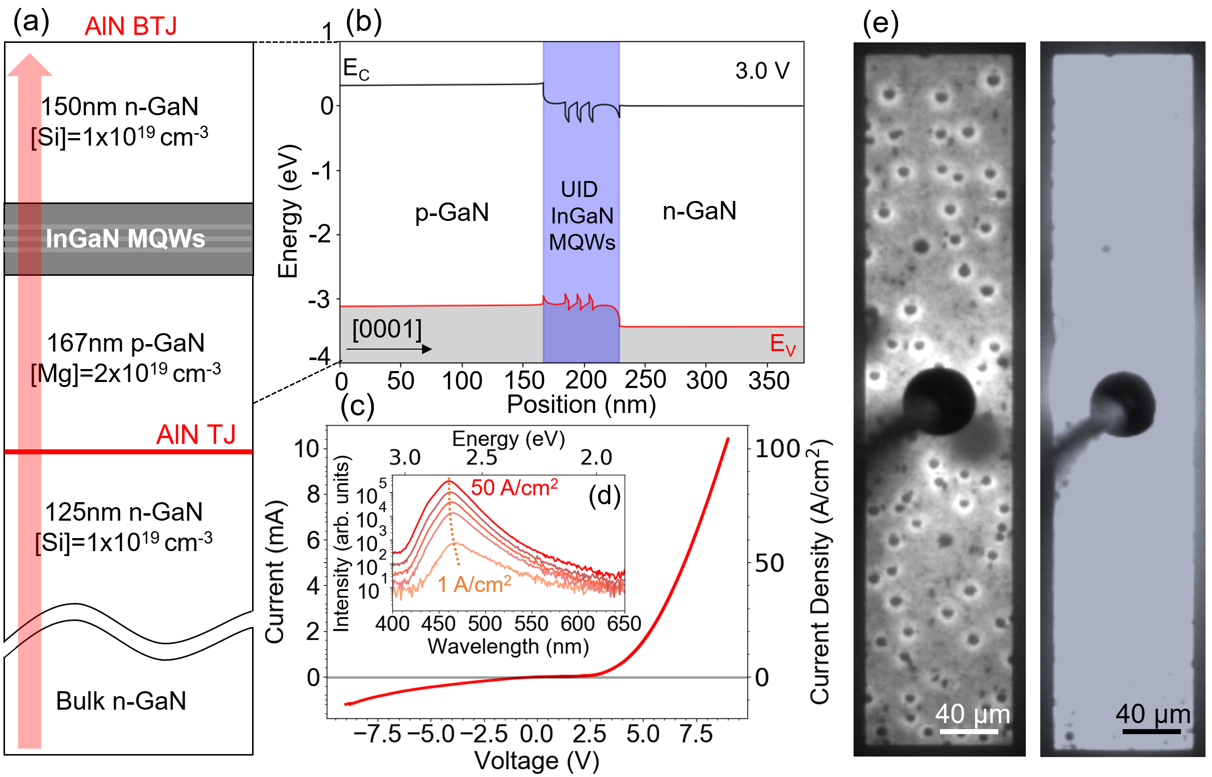
The measurements reported here are performed on blue InGaN LEDs grown by plasma-assisted molecular beam epitaxy (PA-MBE) on c-plane Ge-doped bulk GaN substrates with dislocation density cm-2. The specific growth details and characterization are described in Lee et al. (2020). The two LEDs are buried tunnel homojunction (n-p-i-n) and AlN-interlayered tunnel junction (n-i-p-i-n) structures which have identical active regions. For improved hole injection, LEDs using this design rely on interband Zener tunneling Grundmann and Mishra (2007). The latter also exploits polarization-induced band realignment at the tunnel heterojunctions to enhance the tunneling current Simon et al. (2009). Moreover, with low-resistance n-contacts both on the top and bottom electrodes, the design of these LEDs shows enhanced current spreading compared to a p-i-n LED, making it possible to do spatially resolved electroluminescence measurements. Both of the LEDs show similar inhomogeneity dimensions and density and most of the measurements reported here are done on the AlN-interlayered LED. Figure 1(a)-(b) shows the quantum heterostructure of the AlN-interlayered LED and the energy band diagram of the p-i-n segment at 3.0 V forward bias simulated by SiLENSe. All grown n-type GaN layers are Si-doped with a concentration of [Si]=1019 cm-3, where the p-GaN is Mg-doped with a concentration of [Mg]= cm-3. From bottom upwards, the unintentionally doped (UID) active region consists of a 22 nm In0.07Ga0.93N cladding layer, followed by three periods of 2.8 nm In0.15Ga85N quantum wells/7 nm In0.07Ga0,83N barriers, with an 18 nm In0.07Ga0.93N cladding layer on top. The diode current-voltage characteristics shown in figure 1(c) indicate a forward turn on above 2.5 V and successful implementation of the buried tunnel junction. The resulting MQW electroluminsecence peak emission is at nm or eV at room temperature as seen in Figure 1(d) for various injection currents. Figure 1(e) shows optical microscope images of a 500100 m2 device with a first type of inhomogeneity clearly visible at 20 A/cm2 as spots. The emission becomes increasingly uniform at higher current densities of 50 A/cm2, which is further evidenced by Figure 2(c) which shows that these inhomogeneities brighten with respect of the rest of the (homogeneous) region of the LED as a function of current.
Spatially resolved electroluminescence measurements were performed at room temperature with a silicon photodiode detector. The collection area diameter, , is limited by a optical magnification and silica optical fiber core diameter of 50 m, resulting in m. Monochromatic and spectrally-resolved cathodoluminescence maps were acquired with a Gatan MonoCL4 system using a high-sensitivity photomultiplier and a charge-coupled device as detectors. Using a 300 lines/mm grating and slits of 0.5 mm width, the spectral resolution can be estimated to be 5 nm. The system is mounted to a Zeiss Ultra55 scanning electron microscope operated at an acceleration voltage of 5–7 kV and equipped with a liquid-He cold-stage for measurements at cryogenic temperatures. The spectral maps were analyzed using the python package HyperSpy Peña et al. (2020). The spatial resolution is limited by the scattering of incident electrons and diffusion of excited carriers, which amounts to a few tens of nm.
We first analyse the largest inhomogeneity, which we call type I, as shown in the optical microscope image of the LED under electrical injection in Figure 2(b) and the monochromatic cathodoluminescence maps at the quantum well emission wavelength in Figure 2(d) and Table 1. They manifest as circular spots ranging from m in diameter at a density of cm-2. Local electroluminescence spectra taken at 300K are shown in Figure 2(a) with corresponding collection area in and off the defect indicated by the circles in 2(b), as well as the hyperspectral linescan by cathodoluminescence shown in 2(e) with representative spectra in and off the defect shown in 2(f). Clearly, The quantum well emission is blueshifted within the defect by meV ( nm to nm) relative to the spatially integrated peak at room temperature. We postulate that the blueshift is due to a perturbation of the active region that results from a decreased indium incorporation and reduced quantum well thickness in the region of the type I inhomogeneity. First, we discuss the perturbation due to a compositional variation. It is well known that the bandgap for the ternary InxGa1-xN can be accurately described by a modified Vegard’s law that exhibits a linear as well as quadratic dependence on the indium incorporation . Specifically, the bandgap energy for InxGa1-xN follows the equation:
| (1) |
where is the bandgap of InN (0.65 eV at room temperature) and is the bandgap of GaN (3.4 eV at room temperature), and is the bowing parameter for wurtzite InGaN. It has been shown that the value of b strongly depends on whether the InGaN grown on GaN is strained (b eV) or relaxed (b eV) Orsal et al. (2014). The perturbation to the quantum well transition energy in the inhomogeneous region with reduced indium incorporation compared to the rest of the (homogeneous) LED, is approximately equal to:
| (2) |
where the terms depending quadratically on the composition are neglected for low indium incorporated quantum wells. On the other hand, the conduction and valence band bound energy eigenvalues in the quantum well can be approximated by the solutions to finite potential wells. The exact solution to Schrödinger equation of the finite well ground state energy follows the relation:
| (3) |
where is the ground state energy of the conduction band or valence band electron, and are the barrier and well conduction band minimum or valence band maximum, is the electron or hole effective mass, and is the quantum well thickness. The energy band offset is larger for the conduction band than for the valence band and we make the approximation that the ratio between those offsets is 7:3. This implicit equation for can be separated by making an approximation in which the cosine term on the right side of Equation 3 is approximated by a polynomial de Alcantara Bonfim and Griffiths (2005):
| (4) |
Solving for the electron and hole ground state eigenvalues and then yields:
| (5) |
where are the electron and hole effective mass and is defined as with and for the conduction band and valence band, respectively.
The combined effect of both decreasing the indium incorporation as well as shrinking the quantum well thicknesses increases the emission energy within the type I defect compared to the rest of the LED, as seen in Figure 2(a). Given equations 2 and 5, we approximate the 120 meV energy shift due the effect of reduced indium incorporation or reduced quantum well thickness. The long emission wavelength of 460 nm for the quantum wells suggests the InGaN is relaxed. By equation 2 and using eV, the sole effect of a reduction of indium incorporation leads to , reducing the quantum well indium content from % to %. On the other hand, by equation 5, using and where is the free electron mass, the 120 meV blueshift by thinning of the quantum wells alone is calculated. This would result in a significant reduced well thickness of nm in the type I defect, resulting in nm. Hence, and nm.
This is in fair congruence with LED heterostructure simulations performed using SiLENSe, where the quantum confined Stark effect (QCSE) arising from polarization fields is taken into account as well. The energy-shift then corresponds to and nm. It must be noted that this type of inhomogeneity differs in nature from nanoscopic emission inhomogeneities which are in part responsible for spectral broadening, as well as microscopic emission inhomogeneities on the smaller order of meV. Both can also be explained by compositional fluctuations as well as quantum well monolayer thickness variations. The nanoscopic fluctuations have been held responsible for the high efficiency achieved in quantum well based InGaN blue LEDs, whereas the microscopic fluctuations are in general not desirable Yang et al. (2014); Sakaki et al. (2019).
The type I inhomogeneity is postulated to originate from altered InGaN growth conditions at the location of indium droplets. Such droplets are known to form during PA-MBE under metal (indium) rich growth conditions. Zheng et al. have identified the formation and movement of In droplets on the c-plane growth surface Zheng et al. (2018). The reported size of the droplets coincide with the size of the type I inhomogeneities discussed here. To confirm this observation, an independent MQW sample was grown with the same indium incorporation in its cladding, quantum well and barrier layers as the LED structure, but with no GaN layer on top, and where the indium droplets were deliberately not desorbed, as indicated in Figure 3(a). Indeed, Figure 3(b) shows that the density and size of the type I inhomogeneities are in congruence with the density and size of indium droplets observed on the surface of the sample in Figure 3 (a). Furthermore, AFM scans of the surface of the processed LED shown in Figure 1(a) in the region of the type I inhomogeneity show a circular depression. The surface morphology is often wavy leading towards and into the type I inhomogeneity, which is highlighted by the dashed circle in figure 3(c). This is likely indicative of the indium droplet migrating during growth of the InGaN layers. The wavy nature is due to the 150 nm n-GaN contact layer grown on top of the top InGaN cladding layer. The rough slanted line is a scratch caused by a probe during electroluminescence measurements, and it also serves as a marker to identify the relative position of the inhomogeneity. The observed morphology, along with the blueshift of the type I inhomogeneity then suggest that the incorporation of In and the growth rate are indeed decreased in the region of an indium droplet during the growth of the InGaN active region.

A model for the variation of the indium composition and growth rate is now discussed. It is well known that the indium incorporation x in PAMBE-grown InGaN follows the relation
| (6) |
where and are the incident gallium and incorporated nitrogen fluxes respectively Monroy et al. (2003); Siekacz et al. (2008). The nitrogen that actually incorporates into InGaN, , is approximately equal to the supplied nitrogen flux only for low indium compositions ( 10%). This is because the decomposition of InGaN depends exponentially on an activation barrier, which is larger for GaN (3.6 eV) than InN (1.92 eV) Averbeck and Riechert (1999); Grandjean et al. (1999); Gallinat et al. (2009). Furthermore, the gallium adlayer present during 2D growth does not desorb at the 660 ∘C temperature used for metal rich growth for the active region of the LEDs He et al. (2006). Hence, all of the incident Ga in Equation 6 is incorporated. For high / ( 0.9), corresponding to low indium composition InGaN growth, this then means that the incident nitrogen flux can be approximated to be completely incorporated into InGaN. However, this is not true for lower / where there will be a nitrogen excess.
Indeed, Turski et al. have shown that at low gallium fluxes, initially formed InN bonds are susceptible to decomposition. The released nitrogen can either become part of the incident nitrogen flux and form another InN or GaN bond with adjacent indium or gallium adatoms, or evaporate and be lost indefinitely Turski et al. (2013). Hence, there will be a nitrogen excess such that . Finally, it is important to note that for the metal rich growth condition () for a given growth temperature , the growth rate is determined by . We employ this as given knowledge to explain the growth of the InGaN MQWs underneath the indium droplet and the origin of the blueshift.
First, it should be a justifiable assumption that the gallium flux is not reduced underneath the indium droplet since the diffusion length of gallium adatoms is large in the 2D growth mode Skierbiszewski et al. (2004). The behavior of the measured cladding (Cl) peak by cathodoluminescence at nm or 3.2 eV, as indicated by middle the black arrow in the hyperspectral linescan in Figure 2(e), provides an important clue to understand the growth dynamics underneath the droplet. First and foremost, this peak is not visible in the electroluminescence spectrum at any measured injection current density because of the enhanced injection efficiency and negligible carrier overflow for the inverted LED structure Bharadwaj et al. (2020); van Deurzen et al. (2021). However, from the low temperature cathodoluminescence data, the nm peak from the In0.07Ga0.93N cladding layers are visible, but their emission energy is not blueshifted compared to the homogeneous region of the LED. The two InGaN peaks are labeled in Figure 2(c) by the grey arrows. This discrepancy in energy-shift between the two InGaN peaks suggests that the growth environment underneath the indium droplet is only changed for the MQW which have a higher indium composition In0.15Ga0.85 and not in the barriers and cladding layers. Specifically, this implies that the reincorporation of nitrogen atoms stemming from decomposed InN bonds is reduced underneath the droplet compared to the rest of the LED, resulting in a reduced and increased /, explaining the reduced growth rate and indium incorporation of the quantum wells underneath the droplet.
As a potential explanation, the surface underneath the droplets becomes increasingly nitrogen rich and enhances the formation of molecular , which, unlike the atomic or ionic Nitrogen, is not an active growth species. This reduces the reincorporation of N with In to form InN. The altered active region and growth conditions due to the indium droplets are illustrated in Figure 4.

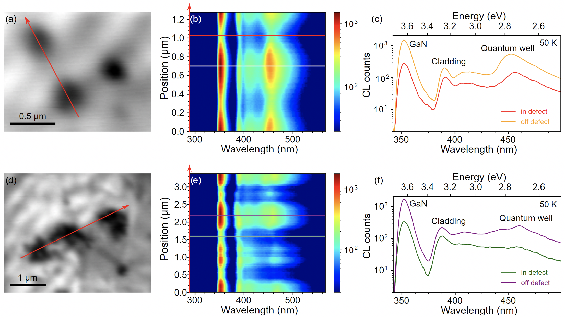
From the density and size of the type I inhomogeneities, they are calculated to cover % of the LED area. This is significant enough to undesirably broaden the spatially-integrated spectrum of the LED, especially at higher normalized current densities, as can be seen from the shoulder in the log-scale spatially-integrated emission spectrum in Figure 1(d). Furthermore, the type I region is transparent to the modes for stimulated emission in a Laser Diode, reducing its gain. The right inset of Figure 2(c), which shows the ratio of the emission intensity on and off the defect, suggests that the droop in the homogeneous region occurs earlier than the droop in the type I region as a function of the normalized current density. This is due to the fact that the current density in the type I region is lower for any given total current as it has a larger bandgap, essentially forming a ’quantum hill’. The density of droplet-related defects can be minimized by using an optimal indium flux during growth. On the other hand, due to growth temperature fluctuations or instability, complete removal of this defect for indium-rich growth is challenging. Another interesting observation about the type I inhomogeneities is the correlation of their location with dislocations that are revealed by hot potassium hydroxide (KOH) etching, as shown by the optical microscope image of the LED in its in Figure 5(a) and (b). The KOH etch was performed at 200 ∘C for 10 minutes Xu et al. (2002). Specifically, most of the type I inhomogeneities that correlate to chemical etch pits correspond to mixed type dislocations such as the one imaged by AFM in Figure 5(c). Zheng et al. have reported that the location of indium droplets are correlated with dislocation density for MBE growth, again suggesting that the type I defects are due to indium droplets Zheng et al. (2018). It is uncertain whether the droplets form at the location of the dislocation or form elsewhere and migrate along the growth surface to eventually be pinned at the dislocation due to strain fields, or both. The latter mechanism can explain the observed wavy morphology shown in Figure 3(c). The correlation suggests that the surface energy of the droplets is reduced at the location of the dislocation due to the strain fields of those dislocations. From another LED grown on a bulk GaN substrate with a lower specified dislocation density of cm-2, the type I density is reduced to = cm-2. This further corroborates that the indium droplet density positively correlates with the dislocation density of the substrate.


Next, we discuss another type of inhomogeneity, which we refer to as type II. They manifest as smaller (than type I) dark spots of diameter m under current injection. The discernable (larger) type II dark spots are indicated by green circles in Figure 5. From cathodoluminescence, the density of type II spots is measured to be cm-2. AFM scans in the region of the type II defects prior to KOH etching indicate that the surface morphology is that of a spiral with star-shaped extensions, as shown by the green square in 5(d). This morphology is known to correspond to screw dislocations for MBE-grown GaN Qian et al. (1995); Heying et al. (1999). However, after etching, merely a small fraction of the screw dislocations show up as V-pits in Figure 5(b), meaning that the KOH etch at 200 ∘C for 10 minutes is not optimized to reveal V-pits corresponding to screw dislocations. An interesting observation is that these screw dislocations are dark in the electroluminescence maps but not always in the cathodoluminescence maps at the quantum well emission energy. Figure 6(a)-(b) shows the quantum well spectrum in and off the defect under electrical injection at 50 A/cm2. The intensity is damped within and around the defect and the ratio of output intensity relative to the rest of the LED does not change as a function of current, as shown in Figure 6(c). This suggests that the center of the type II defect is truly dark in EL and the collected spectrum at these positions is background from the rest of the LED since the size of the collection area is similar to the size of the type I spot. On the other hand, the type II defects display a hexagonal star-like appearance in maps of the QW emission taken by cathodoluminescence, as shown in Figure 6(d) and Table 1. Figures 6(d)–(f) show an integrated intensity map, hyperspectral linescan and selected emission spectra of a dark type II inhomogeneity respectively, taken by cathodoluminescence. It is noticed that in general, the type II is not C6 symmetric and we can define its shape by two axes, which we call the short and long arm as indicated in Figure 6(d) by the white double arrows. The arms can clearly be attributed to the ridges of the hillocks as can be seen from the AFM scan in Figure 5(d), showing the surface morphology of two type II defects. From this figure, it is clear that the asymmetry is due to atomic steps and a local miscut of the sample surface. The measured short and long arms range from 0.56 m to 1.82 m and 0.96 m to 2.25 m, respectively. This ridge formation on the c-plane surface and its dependence of the miscut angle and relation to dislocations has been discussed in GaN grown by metal organic vapor phase epitaxy (MOVPE) Oehler et al. (2013). Figures 6(e) and (f) show that the intensity of the InGaN peaks within the arms are damped compared to off the arms. Another interesting observation is that the intensity of the GaN peak is not damped as strongly as the InGaN peaks and a that there is a slight energy-shift of the InGaN peaks at the center of the defect and within the arms. For the center and the arms, indium segregation could happen due to growth on the hillock facets. At the center, the energy shift of the InGaN peaks could also be explained by indium segregation due to the strain fields induced by the screw dislocation Lei et al. (2010); Horton et al. (2015). Some of the type II defects do not exhibit damped InGaN peaks at the arms and center, yet others exhibit only a dark center in the cathodoluminescent state. The dark center could indicate that they are in fact mixed type dislocations where the dark center is due to non-radiative recombination as described in the following paragraph. Other potential explanations for the dark center are that they are a result of different radiative properties depending on the core structure of the screw dislocation or the presence of voids.
The difference seen in the radiation properties from electroluminescence and cathodoluminesncence is a result of the distinct nature of the transport of electrons and holes in the two methods of excitation. In electroluminescence, the electrons and holes are injected by drift and diffusion into the quantum wells from the opposite ends of the active region through the doped cladding layers and generated by thermal excitation from dopants. In cathodoluminescence, the electron-hole pairs are generated locally by the inverse photoelectric effect and diffusion towards the active region occurs in the same direction, allowing for electrons and holes to be injected into the active region. Hence, the reason for suppressed emission in the electroluminescent state stems from an alteration of the electronic properties of the doped GaN cladding layers, limiting the transport of holes and/or electrons to the active region by electrical injection alone. Specifically, Usamie et al. and Nakano et al. have proven that Mg diffuses along threading screw dislocations (TSDs) and forms a Mg-TSD complex that turns p-type GaN into n-type Usami et al. (2019); Nakano et al. (2020). Depending on the diffusion length of magnesium along the threading screw dislocation into the unintentionally doped InGaN active region and the electronic properties of the Mg-screw complex in InGaN, the p-i-n LED will be converted to n-i-n or n-n-n in the vicinity of the threading screw dislocation, limiting the amount of holes in the active region for radiative recombination and (in the n-n-n case) forming leakage paths.
We next discuss the more prevalent type III inhomogeneity that manifests as small dark regions throughout the LED cladding layers and active region with a diameter m and a density of cm-2. The measurements in Figure 7(a)–(c) show an integrated intensity map, hyperspectral linescan and selected spectra for an area of the LED consisting of three isolated type III defects taken by cathodoluminescence. Within the type III region, all peaks in the spectrum of the LED are quenched. The type III inhomogeneities are too small to be resolved by the localized electroluminescence setup used in this work. Since the density is a factor of larger than the type II screw dislocation density , we attribute the type III to edge dislocations, because the elastic energy of edge dislocations is lower than for screw dislocations Elsner et al. (1997). The reason for the suppressed emission around the threading edge dislocation can then be explained by the formation of non-radiative recombination centers at the threading dislocation in both GaN and InGaN Yao et al. (2020); Bojarska-Cieślińska et al. (2021); Lähnemann et al. (2020). Regions in which multiple type III defects bunch together and form clusters are also observed. For these defects, similar quenching of the peaks is observed, yet in a larger radius around the center of the defect. This is evidenced by the cathodoluminescence measurements that are shown in Figure 7(d)–(f).
Finally, we discuss a fourth type of inhomogeneity, type IV. They come at a density of cm-2 and their diameters range from 10 m m. Panchromatic images of type IV defects under current injection are shown by the blue circle in 5(a) as well as in Table 1. Similar to type II, the intensity is damped in the electroluminescent state but not the cathodoluminescent state, suggesting that the InGaN active region is radiatively intact, but the electronic characteristics of the doped GaN cladding layers are altered in this region. Besides the much larger size, the differences between the type IV with respect to type II, are i) that, similar to type I, the electroluminescence intensity increases with injection current and ii) its etch pit profile. Shown with the blue arrow in Figure 5(b) is the KOH-etched surface of a type IV defect, corresponding to the blue circle in 5(a). Clearly, the etch rate is increased and a cluster of V-pits appear in the region of the type IV, indicating dislocation bunching. Possible explanations for the observed radiative behavior could include the altered doping characteristics of Mg due to the Mg-TSD complex, reduced Si or Mg incorporation in the doped layers in this region, tunnel junction inhomogeneities or reduced mobility of mobile carriers and hence reduced current densities due to scattering by the high density of threading dislocations. As an alternative explanation, the type IV might be due to surface damage resulting from processing the LED, resulting in the increased KOH etch rate.
In summary, as indicated in Table 1, we have identified four types of dislocation-correlated emission inhomogeneities that manifest in InGaN LEDs grown by MBE:
Type I are unique to MBE-grown LEDs and are indium droplet related alterations of the active region which result in a blueshift of the peak quantum well emission. Their location is correlated with mixed type dislocations. With a reduced indium incorporation and thinner quantum wells which results in a larger bandgap, the turn-on voltage is increased and current density is reduced in this region.
Type II are screw dislocations for which the quantum well emission is dark in electroluminescence, but only slightly damped in cathodoluminescence for some defects, and is due to the altered electronic properties of the p-GaN.
Type III are edge dislocations which are dark both in cathodoluminescence and electroluminescence, though with a much smaller radius, due to non-radiative recombination.
Type IV exhibits a large region of suppressed electroluminescence radiation and is revealed to be a region of a high density of dislocations.
An unresolved question in III-Nitride semiconductor heterostructures used in photonic devices is the discrepancy between the internal quantum efficiencies (IQE) of MBE-grown compared to MOCVD-grown spontaneous emitters such as LEDs. This work indicates that the effect of the inhomogeneities reported here, and in particular dislocations, have a merely a slight effect on the overall IQE of the blue InGaN LED. Specifically, type I broadens the J-IQE curve compared to a hypothetical LED without the inhomogeneity, where type II to IV are not unique to MBE-grown LEDs. From the measured intensity spectra and densities of the inhomogeneities, type II and III combined are calculated to reduce the IQE of the LED by 4 compared to a hypothetical LED with no dislocations. Hence, the discrepancy in IQE is likely related to point defects, impurities or an unidentified complex. Recent advancements in N-polar MBE growth have shown a substantial improvement in IQE of photonic structures by increasing the growth temperature and employing nitrogen-rich conditions Turski et al. (2019). This new, exotic approach re-enables the use of N-polar substrates for nitride emitters. Moreover, due to the lack of an indium wetting layer during growth, conducting such process is simpler and similar to MOVPE. Though the IQEs of MBE-grown nitride heterostructures have been low compared to those grown by MOCVD, certain advantages such as buried Mg-doped p-type GaN layers, and higher indium incorporation due to lower growth temperatures offer some unique capabilities in the future, if the low IQE problem can be overcome in a reproducible manner.
The authors acknowledge support from the Cornell Center for Materials Research with funding from the NSF MRSEC program (No. DMR-1719875) and AFOSR Hybrid Materials MURI under Award No. FA9550-18-1- 0480. The authors further acknowledge the Cornell NanoScale Facility for device fabrication, supported by the National Science Foundation with grant No. NNCI-1542081 and RAISE-TAQS 1839196, as well as MRI 1631282.
References
- Sun et al. (2017) M. Sun, Y. Zhang, X. Gao, and T. Palacios, IEEE Electron Device Letters 38, 509 (2017), ISSN 1558-0563, number: 4 Conference Name: IEEE Electron Device Letters.
- Kruszewski et al. (2014) P. Kruszewski, P. Prystawko, I. Kasalynas, A. Nowakowska-Siwinska, M. Krysko, J. Plesiewicz, J. Smalc-Koziorowska, R. Dwilinski, M. Zajac, R. Kucharski, et al., Semiconductor Science and Technology 29, 075004 (2014), ISSN 0268-1242, number: 7 Publisher: IOP Publishing.
- Cao and Arthur (2004) X. A. Cao and S. D. Arthur, Applied Physics Letters 85, 3971 (2004), ISSN 0003-6951, number: 18 Publisher: American Institute of Physics.
- Disney et al. (2013) D. Disney, H. Nie, A. Edwards, D. Bour, H. Shah, and I. C. Kizilyalli, in 2013 25th International Symposium on Power Semiconductor Devices IC’s (ISPSD) (2013), pp. 59–62, iSSN: 1946-0201.
- Skierbiszewski et al. (2005) C. Skierbiszewski, P. Perlin, I. Grzegory, Z. R. Wasilewski, M. Siekacz, A. Feduniewicz, P. Wisniewski, J. Borysiuk, P. Prystawko, G. Kamler, et al., Semiconductor Science and Technology 20, 809 (2005), ISSN 0268-1242, publisher: IOP Publishing.
- Cich et al. (2012) M. J. Cich, R. I. Aldaz, A. Chakraborty, A. David, M. J. Grundmann, A. Tyagi, M. Zhang, F. M. Steranka, and M. R. Krames, Applied Physics Letters 101, 223509 (2012), ISSN 0003-6951, publisher: American Institute of PhysicsAIP.
- Bharadwaj et al. (2020) S. Bharadwaj, S. Bharadwaj, J. Miller, K. Lee, J. Lederman, M. Siekacz, H. G. Xing, H. G. Xing, H. G. Xing, D. Jena, et al., Optics Express 28, 4489 (2020), ISSN 1094-4087, number: 4 Publisher: Optical Society of America.
- Lee et al. (2020) K. Lee, S. Bharadwaj, Y.-T. Shao, L. van Deurzen, V. Protasenko, D. A. Muller, H. G. Xing, and D. Jena, Applied Physics Letters 117, 061104 (2020), ISSN 0003-6951, number: 6 Publisher: American Institute of Physics.
- Mikawa et al. (2020) Y. Mikawa, T. Ishinabe, Y. Kagamitani, T. Mochizuki, H. Ikeda, K. Iso, T. Takahashi, K. Kubota, Y. Enatsu, Y. Tsukada, et al., in Gallium Nitride Materials and Devices XV (International Society for Optics and Photonics, 2020), vol. 11280, p. 1128002.
- Miyajima et al. (2001) T. Miyajima, T. Hino, S. Tomiya, K. Yanashima, H. Nakajima, Y. Nanishi, A. Satake, Y. Masumoto, K. Akimoto, T. Kobayashi, et al., physica status solidi (b) 228, 395 (2001), ISSN 1521-3951.
- Cherns et al. (2001) D. Cherns, S. J. Henley, and F. A. Ponce, Applied Physics Letters 78, 2691 (2001), number: 18 tex.publisher: AIP.
- Albrecht et al. (2008) M. Albrecht, J. L. Weyher, B. Lucznik, I. Grzegory, and S. Porowski, Applied Physics Letters 92, 231909 (2008), ISSN 0003-6951, 1077-3118, number: 23.
- Hino et al. (2000) T. Hino, S. Tomiya, T. Miyajima, K. Yanashima, S. Hashimoto, and M. Ikeda, Applied Physics Letters 76, 3421 (2000), ISSN 0003-6951, 1077-3118, number: 23.
- Liu et al. (2016) W. Liu, J.-F. Carlin, N. Grandjean, B. Deveaud, and G. Jacopin, Applied Physics Letters 109, 042101 (2016), number: 4 tex.publisher: AIP Publishing.
- Elsner et al. (1997) J. Elsner, R. Jones, P. K. Sitch, V. D. Porezag, M. Elstner, T. Frauenheim, M. I. Heggie, S. Öberg, and P. R. Briddon, Physical Review Letters 79, 3672 (1997), number: 19 Publisher: American Physical Society.
- Sugahara et al. (1998) T. Sugahara, H. Sato, M. Hao, Y. Naoi, S. Kurai, S. Tottori, K. Yamashita, K. Nishino, L. T. Romano, and S. Sakai, Japanese Journal of Applied Physics 37, L398 (1998), ISSN 1347-4065, number: 4A Publisher: IOP Publishing.
- Lähnemann et al. (2020) J. Lähnemann, V. M. Kaganer, K. K. Sabelfeld, A. E. Kireeva, U. Jahn, C. Chèze, R. Calarco, and O. Brandt, arXiv:2009.14634 [cond-mat, physics:physics] (2020), arXiv: 2009.14634.
- Chichibu et al. (2006) S. F. Chichibu, A. Uedono, T. Onuma, B. A. Haskell, A. Chakraborty, T. Koyama, P. T. Fini, S. Keller, S. P. DenBaars, J. S. Speck, et al., Nature Materials 5, 810 (2006), ISSN 1476-4660, number: 10 Publisher: Nature Publishing Group.
- Mishra et al. (2021) T. P. Mishra, G. J. Syaranamual, Z. Deng, J. Y. Chung, L. Zhang, S. A. Goodman, L. Jones, M. Bosman, S. Gradečak, S. J. Pennycook, et al., Physical Review Materials 5, 024605 (2021), publisher: American Physical Society.
- Usami et al. (2018) S. Usami, Y. Ando, A. Tanaka, K. Nagamatsu, M. Deki, M. Kushimoto, S. Nitta, Y. Honda, H. Amano, Y. Sugawara, et al., Applied Physics Letters 112, 182106 (2018), ISSN 0003-6951.
- Wang et al. (2020) J. Wang, H. You, H. Guo, J. Xue, G. Yang, D. Chen, B. Liu, H. Lu, R. Zhang, and Y. Zheng, Applied Physics Letters 116, 062104 (2020), ISSN 0003-6951, number: 6 Publisher: AIP Publishing LLC AIP Publishing.
- Li et al. (2004) D. S. Li, H. Chen, H. B. Yu, H. Q. Jia, Q. Huang, and J. M. Zhou, Journal of Applied Physics 96, 1111 (2004), ISSN 0021-8979, publisher: American Institute of Physics.
- Usami et al. (2019) S. Usami, N. Mayama, K. Toda, A. Tanaka, M. Deki, S. Nitta, Y. Honda, and H. Amano, Applied Physics Letters 114, 232105 (2019), ISSN 0003-6951, publisher: American Institute of Physics.
- Nakano et al. (2020) T. Nakano, Y. Harashima, K. Chokawa, K. Shiraishi, A. Oshiyama, Y. Kangawa, S. Usami, N. Mayama, K. Toda, A. Tanaka, et al., Applied Physics Letters 117, 012105 (2020), ISSN 0003-6951, publisher: American Institute of Physics.
- Grundmann and Mishra (2007) M. J. Grundmann and U. K. Mishra, physica status solidi c 4, 2830 (2007), ISSN 1610-1642.
- Simon et al. (2009) J. Simon, Z. Zhang, K. Goodman, H. Xing, T. Kosel, P. Fay, and D. Jena, Physical Review Letters 103, 026801 (2009), ISSN 0031-9007.
- Peña et al. (2020) F. d. l. Peña, E. Prestat, V. T. Fauske, P. Burdet, T. Furnival, P. Jokubauskas, M. Nord, T. Ostasevicius, K. E. MacArthur, D. N. Johnstone, et al., hyperspy/hyperspy: Release v1.6.1 (2020).
- Orsal et al. (2014) G. Orsal, Y. E. Gmili, N. Fressengeas, J. Streque, R. Djerboub, T. Moudakir, S. Sundaram, A. Ougazzaden, and J. P. Salvestrini, Optical Materials Express 4, 1030 (2014), ISSN 2159-3930, publisher: Optical Society of America.
- de Alcantara Bonfim and Griffiths (2005) O. F. de Alcantara Bonfim and D. J. Griffiths, American Journal of Physics 74, 43 (2005), ISSN 0002-9505, publisher: American Association of Physics Teachers.
- Yang et al. (2014) T.-J. Yang, R. Shivaraman, J. S. Speck, and Y.-R. Wu, Journal of Applied Physics 116, 113104 (2014), ISSN 0021-8979, publisher: American Institute of Physics.
- Sakaki et al. (2019) A. Sakaki, M. Funato, M. Miyano, T. Okazaki, and Y. Kawakami, Scientific Reports 9, 3733 (2019), ISSN 2045-2322.
- Zheng et al. (2018) X. Zheng, H. Liang, P. Wang, X. Sun, Z. Chen, T. Wang, B. Sheng, Y. Wang, L. Chen, D. Wang, et al., Superlattices and Microstructures 113, 650 (2018), ISSN 0749-6036.
- Monroy et al. (2003) E. Monroy, N. Gogneau, D. Jalabert, E. Bellet-Amalric, Y. Hori, F. Enjalbert, L. S. Dang, and B. Daudin, Applied Physics Letters 82, 2242 (2003), ISSN 0003-6951, publisher: American Institute of Physics.
- Siekacz et al. (2008) M. Siekacz, A. Feduniewicz-Żmuda, G. Cywiński, M. Kryśko, I. Grzegory, S. Krukowski, K. E. Waldrip, W. Jantsch, Z. R. Wasilewski, S. Porowski, et al., Journal of Crystal Growth 310, 3983 (2008), ISSN 0022-0248, number: 17.
- Averbeck and Riechert (1999) R. Averbeck and H. Riechert, physica status solidi (a) 176, 301 (1999), ISSN 1521-396X.
- Grandjean et al. (1999) N. Grandjean, J. Massies, F. Semond, S. Y. Karpov, and R. A. Talalaev, Applied Physics Letters 74, 1854 (1999), ISSN 0003-6951, publisher: American Institute of Physics.
- Gallinat et al. (2009) C. S. Gallinat, G. Koblmüller, and J. S. Speck, Applied Physics Letters 95, 022103 (2009), ISSN 0003-6951, publisher: American Institute of Physics.
- He et al. (2006) L. He, Y. T. Moon, J. Xie, M. Muñoz, D. Johnstone, and H. Morkoç, Applied Physics Letters 88, 071901 (2006), ISSN 0003-6951, publisher: American Institute of Physics.
- Turski et al. (2013) H. Turski, M. Siekacz, Z. R. Wasilewski, M. Sawicka, S. Porowski, and C. Skierbiszewski, Journal of Crystal Growth 367, 115 (2013), ISSN 0022-0248.
- Skierbiszewski et al. (2004) C. Skierbiszewski, Z. Wasilewski, M. Siekacz, A. Feduniewicz, B. Pastuszka, I. Grzegory, M. Leszczynski, and S. Porowski, physica status solidi (a) 201, 320 (2004), ISSN 1521-396X.
- van Deurzen et al. (2021) L. van Deurzen, S. Bharadwaj, K. Lee, V. Protasenko, H. Turski, H. G. Xing, and D. Jena, in Light-Emitting Devices, Materials, and Applications XXV (International Society for Optics and Photonics, 2021), vol. 11706, p. 117060F.
- Xu et al. (2002) X. Xu, R. P. Vaudo, J. Flynn, and G. R. Brandes, Journal of Electronic Materials 31, 402 (2002), ISSN 1543-186X.
- Qian et al. (1995) W. Qian, G. S. Rohrer, M. Skowronski, K. Doverspike, L. B. Rowland, and D. K. Gaskill, Applied Physics Letters 67, 2284 (1995), ISSN 0003-6951, publisher: American Institute of Physics.
- Heying et al. (1999) B. Heying, E. J. Tarsa, C. R. Elsass, P. Fini, S. P. DenBaars, and J. S. Speck, Journal of Applied Physics 85, 6470 (1999), ISSN 0021-8979, publisher: American Institute of Physics.
- Oehler et al. (2013) F. Oehler, T. Zhu, S. Rhode, M. J. Kappers, C. J. Humphreys, and R. A. Oliver, Journal of Crystal Growth 383, 12 (2013), ISSN 0022-0248.
- Lei et al. (2010) H. Lei, J. Chen, and P. Ruterana, Applied Physics Letters 96, 161901 (2010), ISSN 0003-6951, publisher: American Institute of Physics.
- Horton et al. (2015) M. K. Horton, S. Rhode, S.-L. Sahonta, M. J. Kappers, S. J. Haigh, T. J. Pennycook, C. J. Humphreys, R. O. Dusane, and M. A. Moram, Nano Letters 15, 923 (2015), ISSN 1530-6984, publisher: American Chemical Society.
- Yao et al. (2020) Y. Yao, Y. Sugawara, D. Yokoe, K. Sato, Y. Ishikawa, N. Okada, K. Tadatomo, M. Sudo, M. Kato, M. Miyoshi, et al., CrystEngComm 22, 8299 (2020), publisher: Royal Society of Chemistry.
- Bojarska-Cieślińska et al. (2021) A. Bojarska-Cieślińska, . Marona, J. Smalc-Koziorowska, S. Grzanka, J. Weyher, D. Schiavon, and P. Perlin, Scientific Reports 11, 21 (2021), ISSN 2045-2322, number: 1 Publisher: Nature Publishing Group.
- Turski et al. (2019) H. Turski, A. Feduniewicz-Żmuda, M. Sawicka, A. Reszka, B. Kowalski, M. Kryśko, P. Wolny, J. Smalc-Koziorowska, M. Siekacz, G. Muzioł, et al., Journal of Crystal Growth 512, 208 (2019), ISSN 0022-0248.