Direct thermal infrared vision via nanophotonic detector design
Abstract
Detection of infrared (IR) photons in a room-temperature IR camera is carried out by a two-dimensional array of microbolometer pixels which exhibit temperature-sensitive resistivity. When IR light coming from the far-field is focused onto this array, microbolometer pixels are heated up in proportion to the temperatures of the far-field objects. The resulting resistivity change of each pixel is measured via on-chip electronic readout circuit followed by analog to digital (A/D) conversion, image processing, and presentation of the final IR image on a separate information display screen. In this work, we introduce a new nanophotonic detector as a minimalist alternative to microbolometer such that the final IR image can be presented without using the components required for A/D conversion, image processing and display. In our design, the detector array is illuminated with visible laser light and the reflected light itself carries the IR image which can be directly viewed. We realize and numerically demonstrate this functionality using a resonant waveguide grating structure made of typical materials such as silicon carbide, silicon nitride, and silica for which lithography techniques are well-developed. We clarify the requirements to tackle the issues of fabrication nonuniformities and temperature drifts in the detector array. We envision a potential near-eye display device for IR vision based on timely use of diffractive optical waveguides in augmented reality headsets and tunable visible laser sources. Our work indicates a way to achieve direct thermal IR vision for suitable use cases with lower cost, smaller form factor, and reduced power consumption compared to the existing thermal IR cameras.
I Introduction
Thermal infrared cameras provide images at infrared wavelengths, typically in the long-wave infrared (LWIR) range of to , thus allowing us to transcend the visible-spectrum limitation of human eyes Gade and Moeslund (2014). The infrared cameras consist of an imaging system and infrared detectors of which there are two types, namely photon detectors Tan and Mohseni (2018); Zhuge et al. (2017); LaPierre et al. (2017) and thermal detectors Jayaweera et al. (2008); Kruse (1997). The former rely on the conversion of incident IR photons to electrons by using low-bandgap semiconductor detectors which typically require low cryogenic temperatures. The latter rely on the conversion of incident IR photons to heat using microbolometer detector pixels. The converted heat results into small temperature variations which can then be measured to form an image. Such thermal detectors can operate at or near room temperature. Based on operating temperatures, photon detectors and thermal detectors are also called as cooled and uncooled IR detectors respectively. The advantages of thermal detectors over photon detectors are lower cost, smaller size, lighter weight, lower maintenance, longer lifetime, immediate power-up capability and reduced power consumption, while the disadvantages are lower sensitivity and intrinsically slower response speed (typical time constant of few ). Despite some of these disadvantages, the thermal detectors and cameras are used for an increasing number of cost-sensitive applications that do not necessarily demand high performance and speeds of photon detectors Kimata (2018); Takasawa (2015). Microbolometers are now produced in larger volumes than all other IR detector array technologies together Rogalski (2017).
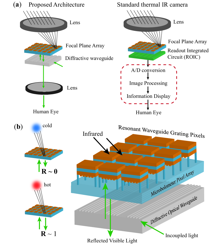
In this work, we introduce a new nanophotonic detector in place of microbolometer to considerably simplify the overall architecture of the thermal IR imaging system, where ‘thermal’ indicates the underlying thermal detector as well as our focus on the detection of LWIR radiation generated thermally in the far-field. Our proposed design is schematically illustrated in the left panel of Fig. 1(a) along with the schematic design of the standard thermal IR imaging system in the right panel (with dimensions not to scale). In both cases, LWIR radiation from the far field is focused by an infrared-transparent lens onto the focal plane array (FPA) which consists of micron-size detector pixels suspended on top of a substrate and designed to be good LWIR absorbers. In the standard design based on bolometers, such a pixel contains a phase change material (e.g. vanadium oxide) having temperature-sensitive electrical resistivity. A bias current is passed through the pixel and the voltage difference across it is measured using a readout integrated circuit (ROIC). The IR-absorption-induced temperature change of the bolometer causes its resistivity to change (typically few ). The resulting voltage change signals measured by ROIC are fed to A/D converters and after additional digital processing, final IR image is presented on a separate information display screen.
Our design is motivated by the idea of directly visualizing the pixel temperature changes relative to the substrate by measuring the reflection of visible light. This will eliminate the need for A/D conversion, image processing, and a separate display screen (red box). In this architecture, visible light is projected onto the array of detector pixels using a diffractive optical waveguide which is used in augmented reality eye-wearables that overlay digital content on top of the real-world scene Kress and Chatterjee (2021). As illustrated in Fig. 1(b), the detector pixel is designed such that large temperature changes relative to the supporting substrate corresponding to hot objects in the far field lead to high reflectivity () while small temperature changes corresponding to cold objects in the far field lead to low reflectivity (). The light reflected from the pixel array is spatially modulated by the map of the temperature changes of the detectors. The diffractive optical waveguide is usually designed with a small diffraction efficiency, such that the reflected light from the pixel array can transmit through the waveguide layer in the perpendicular direction. The resulting temperature map of spot size can be directly viewed through the magnifying lens as shown in Fig. 1(a). While many parts of this optical architecture currently exist, the detector pixel for performing the intended functionality needs to be specially designed, and that is the focus of this work.
We note that optical measurement of thermal IR detector pixels has been explored previously in Refs. Ostrower (2006); Pris et al. (2012); Shen et al. (2018); Watts et al. (2007); Exner et al. (2013); Zhao et al. (2018); Choi et al. (2003). Moreover, Refs. Pris et al. (2012) and Choi et al. (2003) also show the use of charge-coupled device (CCD) imagers to form an image based on light reflected from the detector pixels. In contrast to these works, here we envision that the temperature map on the detector pixel array to be directly viewed by human eyes through a magnifying lens, in order to further simplify the design of thermal imaging systems. For this purpose, we design the pixels to achieve low to high reflectivity change at visible illumination wavelength indicating high contrast between cold and hot objects in the far field as illustrated in Fig. 1(b). Our design utilizes resonant waveguide gratings Rosenblatt et al. (1997); Quaranta et al. (2018) which are different in terms of both geometry and material options from all above-mentioned works Ostrower (2006); Pris et al. (2012); Shen et al. (2018); Watts et al. (2007); Exner et al. (2013); Zhao et al. (2018); Choi et al. (2003) in the context of optical measurement of IR detectors.
The commercial thermal IR cameras, which have matured after many decades of research Rogalski (2017), primarily use bolometers with electronic ROIC measurements. Although comparable or better performance may be achieved, introducing optical measurement instead of electronic readout in this well-established technology is challenging unless there is a significant (order of magnitude) or a distinct technological advantage of doing so. Our work advances this line of research by bringing to attention the unique advantage of optical readout in enabling direct thermal IR vision with a carefully engineered system such that additional components for A/D conversion, image processing, and a separate information display are no longer required. Since electronic readout is not sufficient for presenting the final IR image and these additional components are necessarily required for standard thermal IR cameras, the capability to realize direct thermal IR vision is in principle a distinct advantage of optical readout over electronic readout. Our work can potentially help to further advance the thermal IR imaging technology by reducing the form factor (size, weight), cost, and power consumption. It can pave the way for developing small-size, light-weight eye-wearables that can potentially augment human vision with thermal infrared vision.
II Results
The proposed functionality illustrated in Fig. 1(b) requires each detector pixel to satisfy the following conditions. First, the pixel’s reflectivity at the visible illumination wavelength should change substantially with its temperature changes relative to the substrate. Moreover, it should change from low to high for increasing temperature differentials to indicate contrast between cold and hot objects in the far field. Second, the pixel should be a good absorber around the wavelength of m which corresponds to the peak wavelength of thermal radiation from near-room-temperature bodies. Third, the pixel should have good thermal isolation from its surroundings so that the absorbed thermal radiation can lead to a reasonable change in temperature, typically of the order of few Kelvins compared to the substrate. Fourth, the thermal time constant of the pixel should be small so that the response speed to the temporal variation of the incident thermal radiation is fast. Since the third requirement above limits the thermal conductance of the pixel to the surrounding environment, the thermal mass of the pixel should be sufficiently small. For standard thermal IR cameras, the third requirement is addressed by the suspension of microbolometer pixels on top of a substrate inside vacuum packaging such that the heat exchange occurs primarily via conduction between the detector and the substrate. Additionally, radiation shields are used to prevent any unwanted IR radiation from the packaging which is unrelated to the far-field scene García-Blanco et al. (2017). In the following, assuming the use of vacuum packaging and radiation shields, we describe our nanophotonic design that addresses the four pixel requirements. We also analyze the effects of any spurious temperature drifts and potential fabrication nonuniformity within or across detector pixels on the device performance, and clarify the related requirements and calibration methods to tackle them.
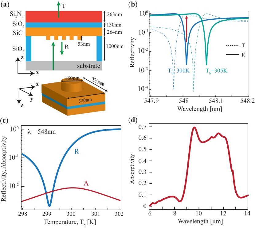
Figure 2(a) illustrates the pixel design (dimensions not to scale). It consists of a multi-layered patterned slab depicted in the top inset consisting of layers of silicon nitride (Si3N4), silicon dioxide (SiO2), silicon carbide (SiC) with patterning in the form of a two-dimensional lattice of cylinders as depicted in the bottom inset. This constitutes a detector pixel which is suspended on top of four insulating posts on a substrate. For calculations below, we assume substrate to be silica glass. The individual layer thicknesses and the lattice periods are mentioned in the schematic in Fig. 2(a). We assume that each pixel is in lateral directions and separated by from the neighboring pixel. Such pixel dimensions are common in photon IR and thermal IR detectors with the latest research reporting pixel sizes down to Rogalski et al. (2016). Since refractive indices of SiC and Si3N4 are larger than that of SiO2 at visible wavelengths, these layers support guided modes which can couple to normally incident light via periodic grating, resulting into sharp resonant features in reflection and transmission spectra Wang and Magnusson (1993); Tibuleac and Magnusson (1997); Fan and Joannopoulos (2002); Crozier et al. (2006). Because the materials are low-loss and transparent in this wavelength range, it is possible to realize high quality factor () resonances. Such guided mode resonance structures also identified as resonant waveguide gratings (RWG) Rosenblatt et al. (1997); Quaranta et al. (2018) and analogous high contrast gratings with slight geometric modifications Chang-Hasnain and Yang (2012) have been well-studied and also used for sensing small changes in refractive index Fang et al. (2006); Xu et al. (2019). However, their use for the optical readout of IR detectors was not previously considered.
Figure 2(b) demonstrates the reflection (solid lines) and transmission (dashed lines) spectra for normal incidence of light around nm and for two different detector temperatures K and K. The small temperature change induced by the absorbed thermal IR signals from the far-field causes a small change in the refractive index via thermo-optic effect. The thermo-optic coefficient of SiC given by is much larger than the coefficients of SiO2 and Si3N4 (of the order of ) Watanabe et al. (2011); Powell et al. (2020). As shown in Fig. 2(b), the high -factor resonant dip in the reflection spectrum shifts noticeably toward larger wavelength upon increasing the pixel temperature. When this structure is illuminated by a laser source close to nm (green light), a large change in the reflectivity is observed as indicated by the red arrow. at changes to at . The temperature dependence of the reflectivity is demonstrated in Fig. 2(c) assuming normal incidence of monochromatic laser light at nm. The plot indicates that the reflectivity increases monotonically as the temperature increases from up to . Thus, if the substrate temperature is fixed at , this specific example system with illumination at nm can be used to sense the differentials of induced by IR absorption. Although we fixed and illumination wavelength for explaining this underlying mechanism, we explain further below that the illumination wavelength can be readily tuned in real time by sensing the substrate temperature such that in the absence of any incident thermal IR signals. We also note that the laser illumination can cause the detector pixel to heat up depending on illumination intensity, pixel area and pixel absorptivity. The proposed structure exhibits low absorptivity () as shown by the red curve in Fig. 2(c). For our specific design, we show below that the heating induced by the laser for typical illumination intensity appropriate for human vision is much smaller than the typical absorbed thermal IR power because of this low absorptivity.
We now discuss the details of our design related to the problem of IR detection. The thicknesses and lattice periods in the proposed design are obtained using optimization informed by the physics of RWG structures as described in the methods section. The example system discussed above is by no means unique, and many solutions at various visible wavelengths can be readily obtained for different geometric parameters (thicknesses and lattice periods) using the same material layers. We also note that this optimization is performed with respect to the optical readout and not with respect to thermal IR absorption. Nonetheless, the proposed pixel structure is already a reasonably good absorber of thermal radiation as shown in Fig. 2(d) which is ensured by the specific choice of materials. In particular, the material choice in our design is governed by the fulfillment of two conditions, namely good infrared photon absorption in range for LWIR detection and low-loss transparent nature at visible wavelengths () for realizing high -resonance to detect small changes in pixel temperature. In microbolometers used in standard thermal IR detectors, Si3N4 is already used because of its broadband LWIR absorption. While SiC and SiO2 also lead to resonant absorption in m due to their optical phonon polaritons, the resulting absorption spectrum is rather narrowband. Therefore, addition of Si3N4 layer in the present design helps enhance and broaden the LWIR absorption. In standard microbolometers, phase-transition materials such as vanadium oxide (VOx) and amorphous silicon (aSi) which exhibit large thermal coefficient of resistance (TCR) of few are typically used. While the same materials also exhibit large thermo-optic effect, they are quite lossy at visible wavelengths. Therefore, these materials as well as metals and metal oxides cannot be used for the intended detector pixel design.
Below, we quantitatively describe the thermal aspects of our nanophotonic design. The temperature of the detector pixel follows the heat equation:
| (1) |
where is the thermal mass given by the product of the mass and the specific heat capacity of each material layer, is the thermal conductance between the pixel and the substrate via insulating posts, is the intensity of the laser illumination, is the absorptivity plotted in Fig. 2(c), is the pixel area, is the absorbed IR power. Using mass densities , , and specific heat capacities , , Adachi (2004), and taking into account volume fractions, we obtain . Assuming four insulating posts of length and cross section , each made of SiO2 of thermal conductivity , thermal conductance is calculated based on Fourier’s law of conduction. While we considered insulating posts for simplicity of this calculation, the bridge structure typically used in standard thermal IR detectors can also be employed without any changes to the detector pixel design. In fact, advances in microelectromechanical systems (MEMS) technology have now enabled using such bridge structures for thermal IR detectors Kimata (2018). The response speed is characterized by the time constant which is for our design. For typical microbolometers, the absorbed thermal power depends on the pixel area , pixel absorptivity plotted in Fig. 2(d), the transmissivity of the lens used for focusing the IR light, temperature and distance of the object emitting the IR light etcetera. Instead of introducing many new parameters here, we refer to the previous work and use the typical values of for typical microbolometers of similar pixel areas which are in the range of tens of nW Svatoš et al. (2018); Ryu et al. (2015).
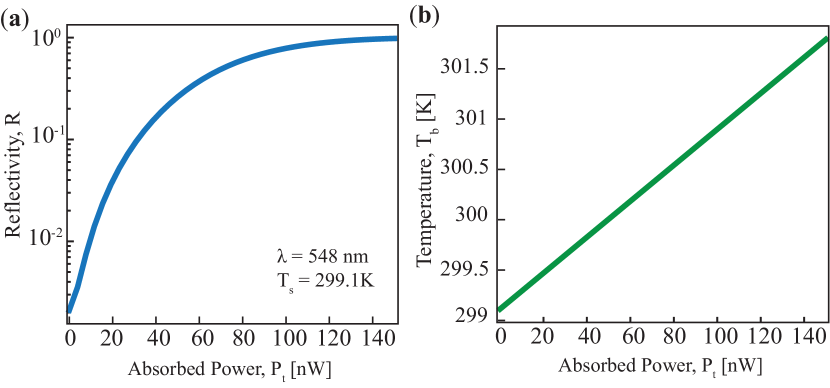
Figure 3(a) depicts the change in the reflectivity for the specific example system analyzed above as a function of absorbed thermal IR power. We assume that the intensity of incident visible light coming from the diffractive optical waveguide is around (approximately similar to the brightness levels of displays like computer monitors). Because of small absorptivity of the pixels of area , the absorbed optical power is which is much smaller than the typical values of absorbed thermal IR power. The heating due to thermal IR absorption leads to small changes in the detector temperature () which is demonstrated in Fig. 3(b). Accordingly, the reflectivity is changed leading to strong reflection corresponding to LWIR radiation coming from hot objects in the far field. We note that the reflectivity changes over wider temperature ranges of can also be engineered with different optimized nanophotonic design. The possible temperature swing of the detector pixel primarily depends on the thermal conductance and the maximum absorbed thermal IR power by the relation . These parameters can be estimated in separate experiments and the design can be iterated to realize optimized performance.
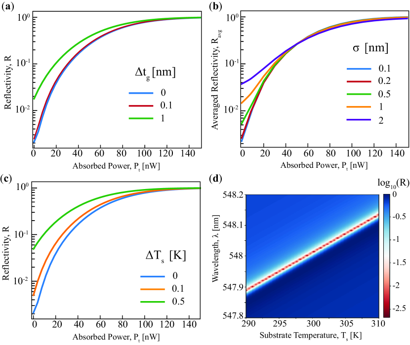
We note that the pixel uniformity across all pixels is important for recreating reliable final IR image of the far-field scene. The proposed design which uses high resonance for refractive index sensing, also responds sensitively to design perturbations. For example, Fig. 4(a) demonstrates the reflectivity dependence on by introducing small perturbation in the thickness of the grating. As evident from the figure, nanometric fabrication variations can cause reflectivity to deviate for small values of . While lattice periods are usually accurate, the grating structures may experience small perturbations even for a single pixel. To address these perturbations, we assume a zero-mean Gaussian-distributed error of standard deviation in the grating thickness for all detector pixels and plot the averaged reflectivity in Fig. 4(b). At small values of , the averaged reflectivity at deviates from the averaged reflectivity for the design with small values of . Although such deviations need to be analyzed for accurate quantitative estimations of temperatures of far-field objects, from the perspective of direct thermal IR vision which is the focus of this work, high contrast and monotonic increase exhibited by the averaged reflectivity of the detector pixels having nanometric fabrication nonuniformity can be considered acceptable. For the proposed design, the detector FPA of pixels will require fabrication precision of at most few standard deviation of surface roughness over area of the device. We note that advances in lithography techniques such as nanoimprint lithography have enabled low-cost fabrication of large-area patterned surfaces Sreenivasan (2017). In a separate work Fan et al. (2020), subnanometer precision in terms of surface roughness of approximately has been realized for SiC on insulator surfaces. Therefore, we believe that fabrication requirements for the proposed design can be ensured using state-of-the-art lithography techniques.
In the design of microbolometer IR detectors, significant importance is given to drifts or small changes in the substrate temperature (). The detector is designed to be highly sensitive to which depends on the absorbed IR power and the substrate temperature . Variation in causes an equal variation in , and this becomes a major source of unwanted signal which is unrelated to IR signals coming from the far field. Various calibration or compensation approaches are used in standard microbolometer IR detectors to tackle this important issue Lv et al. (2014); Nugent et al. (2013). The same holds true for the proposed design. For instance, Fig. 4(c) demonstrates the reflectivity dependence on for small variations in the substrate temperature () for fixed illumination wavelength. Evidently, the deviation in is quite large for small . This problem can be solved by tuning the illumination wavelength in real time based on prior measurements of reflectivity for different values of . The contour plot in Fig. 4(d) illustrates that the illumination wavelength which should coincide with the resonant dip () in the reflectivity spectrum increases linearly with . Such linear tunability can be achieved with on-chip microheaters with integrated tunable visible laser sources Franken et al. (2020); Boller et al. (2020); Malik et al. (2021). While our proposed architecture does not involve electronic readout and digital processing, it will require a thermocouple to measure and a controller system to tune the illumination wavelength in a predetermined manner in real time. An alternative to such a controller system can be temperature stabilization using small Peltier elements used in some versions of thermal IR cameras. On-chip device temperatures can be stabilized within few temperature variations Choi et al. (2003) and the operating wavelength can be fixed to coincide with the resonant dip in the reflectivity spectrum. We note that the fabrication nonuniformity and the temperature drifts can also be mitigated by using illumination light of bandwidth comparable or close to the bandwidth of the resonant dip in the reflection spectrum instead of using monochromatic light. Since the response is integrated (or averaged) over a bandwidth of wavelengths, the sensitivity to unwanted design perturbations is reduced. Aside from the specific detector pixel requirements and considerations related to fabrication and temperature drifts (discussed above), vacuum packaging and radiation shields are required for developing a proof-of-concept thermal IR imaging system. The same packaging solutions used for traditional microbolometer FPAs García-Blanco et al. (2017) can be translated and used for our design.
III Conclusion
We introduced a new nanophotonic detector in place of traditional microbolometer as a viable minimalist approach to thermal IR imaging. Our proposed design produces an IR image as spatially modulated wavefront of reflected visible light which can be directly viewed by the human eye. This design eliminates the need for additional components for electronic readout, A/D conversion, image processing and information display, otherwise necessary in standard thermal IR cameras. The proposed design can be useful for achieving the same functionality as IR cameras potentially at reduced cost, form factor and power consumption. We note that digital processing of electronic or optical measurement of the detector pixels is useful for additional error-compensation techniques and is necessary for providing quantitative estimates (in numbers) of temperatures of far-field objects. A figure of merit called as noise equivalent temperature difference (NETD) is used to compare the performance of IR cameras in their ability to quantify tiny temperature differences between two far-field objects Gade and Moeslund (2014); Rogalski (2017). Our design does not provide such quantitative temperature estimates since it is designed to directly provide an IR image to the human eye. Nonetheless, there can be use cases where the proposed minimalist approach can be potentially employed. For many practical applications of IR cameras such as inspection and detection in industrial, infrastructure, agriculture, healthcare settings, night vision or low-light vision for military, fire-fighters, camping enthusiasts, the objective of the device is to provide an IR image to the human eye. In some of these use cases, the final human evaluation is often based on the IR image and not the temperature numbers, thus requiring strong contrast and good quality of the IR image. Therefore, we believe that the proposed minimalist approach can be practically useful.
Apart from the actual proof-of-concept experimental demonstration,
there are many interesting aspects of this work that can be further
extended in the near future. All components used in the design are
transparent at visible wavelengths. If the optical lenses are
optimized simultaneously for visible and infrared wavelengths to
reduce chromatic aberration, it is conceivable that the final image
will contain IR image at the specific laser illumination wavelength
overlaid on top of the visible image. Such augmented thermal vision
functionality with frugal resources can be an interesting new
technology. One can also design multi-spectral IR imaging where
different IR wavelengths are mapped to different visible wavelengths
using multiple optimized pixels. For example, two types of detector
pixels can be designed to potentially map SWIR () light to
green light and LWIR () light to red light. Such a
functionality is quite challenging to develop even with traditional
microbolometer detectors. We believe that our work paves the way for
developing such novel IR imaging capabilities in the near future.
IV Methods
The permittivities of SiC, SiO2 and Si3N4 are obtained from various references Palik (1998); Luke et al. (2015). The simulation of reflection and transmission is performed using well-known rigorous coupled wave analysis (RCWA) technique Moharam et al. (1995); Jin et al. (2020). The open-source code is available at GRCWA under GPL license. For the calculation of the detector pixel absorptivity of the incident IR radiation plotted in Fig.2(d), we calculate the flux reflected from the pixel and the flux in the vacuum gap between the pixel and the substrate, assuming normal incidence of light. For our nanophotonic design of the pixel as a refractive index sensor, we use the Nelder-Mead method to find the geometric parameters (thickness of each material layer) which minimize the ratio of the reflectivities given by at a fixed wavelength. Because of physics-informed ordering of layers (intended to support guided modes inside SiC and Si3N4 layers), this optimization upon few trials and starting points yields optimized design with and . Additional inverse design constrained and informed by nanofabrication capabilities and costs can certainly be formulated to automate this design with the objective of achieving the reflectivity change from to over a specific temperature differential. This differential is given by where the conductance and the typical absorbed thermal IR power for the detector pixel can be estimated separately for the fabricated design.
V Acknowledgement
C.K. would like to acknowledge helpful discussion with Dr. Bo Zhao regarding the potential use of hexagonal boron nitride (hBN) in our nanophotonic design. This work is supported by a MURI project from the U.S. Air Force Office of Scientific Research (FA9550-21-1-0312).
References
- Gade and Moeslund (2014) R. Gade and T. B. Moeslund, Machine vision and applications 25, 245 (2014).
- Tan and Mohseni (2018) C. L. Tan and H. Mohseni, Nanophotonics 7, 169 (2018).
- Zhuge et al. (2017) F. Zhuge, Z. Zheng, P. Luo, L. Lv, Y. Huang, H. Li, and T. Zhai, Advanced Materials Technologies 2, 1700005 (2017).
- LaPierre et al. (2017) R. LaPierre, M. Robson, K. Azizur-Rahman, and P. Kuyanov, Journal of Physics D: Applied Physics 50, 123001 (2017).
- Jayaweera et al. (2008) P. Jayaweera, S. Matsik, A. Perera, H. Liu, M. Buchanan, and Z. Wasilewski, Applied Physics Letters 93, 021105 (2008).
- Kruse (1997) P. W. Kruse, in Semiconductors and semimetals, Vol. 47 (Elsevier, 1997) pp. 17–42.
- Kimata (2018) M. Kimata, IEEJ Transactions on Electrical and Electronic Engineering 13, 4 (2018).
- Takasawa (2015) S. Takasawa, in Image Sensing Technologies: Materials, Devices, Systems, and Applications II, Vol. 9481 (International Society for Optics and Photonics, 2015) p. 94810H.
- Rogalski (2017) A. Rogalski, in Electro-Optical and Infrared Systems: Technology and Applications XIV, Vol. 10433 (International Society for Optics and Photonics, 2017) p. 104330L.
- Kress and Chatterjee (2021) B. C. Kress and I. Chatterjee, Nanophotonics 10, 41 (2021).
- Ostrower (2006) D. Ostrower, III-Vs Review 19, 24 (2006).
- Pris et al. (2012) A. D. Pris, Y. Utturkar, C. Surman, W. G. Morris, A. Vert, S. Zalyubovskiy, T. Deng, H. T. Ghiradella, and R. A. Potyrailo, Nature Photonics 6, 195 (2012).
- Shen et al. (2018) Q. Shen, Z. Luo, S. Ma, P. Tao, C. Song, J. Wu, W. Shang, and T. Deng, Advanced Materials 30, 1707632 (2018).
- Watts et al. (2007) M. R. Watts, M. J. Shaw, and G. N. Nielson, Nature Photonics 1, 632 (2007).
- Exner et al. (2013) A. T. Exner, I. Pavlichenko, B. V. Lotsch, G. Scarpa, and P. Lugli, ACS applied materials & interfaces 5, 1575 (2013).
- Zhao et al. (2018) Q. Zhao, M. W. Khan, S. Farzinazar, J. Lee, and O. Boyraz, Optics express 26, 29638 (2018).
- Choi et al. (2003) J. Choi, J. Yamaguchi, S. Morales, R. Horowitz, Y. Zhao, and A. Majumdar, Sensors and Actuators A: Physical 104, 132 (2003).
- Rosenblatt et al. (1997) D. Rosenblatt, A. Sharon, and A. A. Friesem, IEEE Journal of Quantum electronics 33, 2038 (1997).
- Quaranta et al. (2018) G. Quaranta, G. Basset, O. J. Martin, and B. Gallinet, Laser & Photonics Reviews 12, 1800017 (2018).
- García-Blanco et al. (2017) S. García-Blanco, T. Pope, P. Côté, M. Leclerc, L. N. Phong, and F. Châteauneuf, in International Conference on Space Optics—ICSO 2008, Vol. 10566 (International Society for Optics and Photonics, 2017) p. 105662V.
- Rogalski et al. (2016) A. Rogalski, P. Martyniuk, and M. Kopytko, Reports on Progress in Physics 79, 046501 (2016).
- Wang and Magnusson (1993) S. Wang and R. Magnusson, Applied optics 32, 2606 (1993).
- Tibuleac and Magnusson (1997) S. Tibuleac and R. Magnusson, JOSA A 14, 1617 (1997).
- Fan and Joannopoulos (2002) S. Fan and J. D. Joannopoulos, Physical Review B 65, 235112 (2002).
- Crozier et al. (2006) K. B. Crozier, V. Lousse, O. Kilic, S. Kim, S. Fan, and O. Solgaard, Phys. Rev. B 73, 115126 (2006).
- Chang-Hasnain and Yang (2012) C. J. Chang-Hasnain and W. Yang, Advances in Optics and Photonics 4, 379 (2012).
- Fang et al. (2006) Y. Fang, A. M. Ferrie, N. H. Fontaine, J. Mauro, and J. Balakrishnan, Biophysical journal 91, 1925 (2006).
- Xu et al. (2019) Y. Xu, P. Bai, X. Zhou, Y. Akimov, C. E. Png, L.-K. Ang, W. Knoll, and L. Wu, Advanced Optical Materials 7, 1801433 (2019).
- Watanabe et al. (2011) N. Watanabe, T. Kimoto, and J. Suda, in Micromachining and Microfabrication Process Technology XVI, Vol. 7926 (International Society for Optics and Photonics, 2011) p. 792604.
- Powell et al. (2020) K. Powell, A. Shams-Ansari, S. Desai, M. Austin, J. Deng, N. Sinclair, M. Lončar, and X. Yi, Optics express 28, 4938 (2020).
- Adachi (2004) S. Adachi, Handbook on physical properties of semiconductors, Vol. 2 (Springer Science & Business Media, 2004).
- Svatoš et al. (2018) V. Svatoš, I. Gablech, J. Pekárek, J. Klempa, and P. Neužil, Infrared Physics & Technology 93, 286 (2018).
- Ryu et al. (2015) S. Y. Ryu, H. Y. Choi, D. U. Kim, G. H. Kim, T. Kim, H. Y. Kim, and K. S. Chang, JSTS: Journal of Semiconductor Technology and Science 15, 533 (2015).
- Sreenivasan (2017) S. Sreenivasan, Microsystems & nanoengineering 3, 1 (2017).
- Fan et al. (2020) T. Fan, X. Wu, A. A. Eftekhar, M. Bosi, H. Moradinejad, E. V. Woods, and A. Adibi, Optics Letters 45, 153 (2020).
- Lv et al. (2014) J. Lv, L. Que, L. Wei, Y. Zhou, B. Liao, and Y. Jiang, IEEE Sensors Journal 14, 1533 (2014).
- Nugent et al. (2013) P. W. Nugent, J. A. Shaw, and N. J. Pust, Optical Engineering 52, 061304 (2013).
- Franken et al. (2020) C. A. Franken, A. van Rees, Y. Fan, D. Geskus, R. Dekker, D. H. Geuzebroek, C. Fallnich, P. J. van der Slot, and K.-J. Boller, arXiv preprint arXiv:2012.04563 (2020).
- Boller et al. (2020) K.-J. Boller, A. van Rees, Y. Fan, J. Mak, R. E. Lammerink, C. A. Franken, P. J. van der Slot, D. A. Marpaung, C. Fallnich, J. P. Epping, et al., in Photonics, Vol. 7 (Multidisciplinary Digital Publishing Institute, 2020) p. 4.
- Malik et al. (2021) A. Malik, C. Xiang, L. Chang, W. Jin, J. Guo, M. Tran, and J. Bowers, Applied Physics Reviews 8, 031306 (2021).
- Palik (1998) E. D. Palik, Handbook of optical constants of solids, Vol. 3 (Academic press, 1998).
- Luke et al. (2015) K. Luke, Y. Okawachi, M. R. Lamont, A. L. Gaeta, and M. Lipson, Optics letters 40, 4823 (2015).
- Moharam et al. (1995) M. Moharam, E. B. Grann, D. A. Pommet, and T. Gaylord, JOSA a 12, 1068 (1995).
- Jin et al. (2020) W. Jin, W. Li, M. Orenstein, and S. Fan, ACS Photonics 7, 2350 (2020).