Design of the Compact Processing Module for the ATLAS Tile Calorimeter
Abstract
The LHC will undergo a major upgrade starting in 2025 towards the High Luminosity LHC (HL-LHC) to increase the instantaneous luminosity by a factor of 5 to 7 compared to the nominal value.
The Phase-II Upgrade (2025–2027) will require the trigger and readout electronics of the ATLAS experiment to operate with the stringent conditions imposed by the HL-LHC. During this upgrade, both on- and off-detector readout electronics of TileCal will be completely replaced with a new data acquisition which will provide full-granularity information to the ATLAS trigger system.
The Compact Processing Modules are responsible for the LHC bunch-crossing clock distribution towards the detector, configuration of the on-detector electronics, data acquisition, cell energy reconstruction, and data transmission to the TDAQ interface (TDAQi).
The CPM has been designed as an AMC form-factor board equipped with 8 Samtec FireFly modules for communication with the detector, a Xilinx Kintex UltraScale FPGA for data acquisition and processing, a Xilinx Artix 7 FPGA for slow control and monitoring, and other subsystems to generate high-quality clocks for the FPGAs and communications.
The high-speed communication with the on-detector electronics is implemented via 32 GigaBit Transceiver links receiving detector data at 9.6 Gbps and transmitting commands and the LHC clock at 4.8 Gbps, while the reconstructed cell energies are transmitted to TDAQi via 4 FULL-mode links. Triggered data is transmitted through a FULL-mode link to the ATLAS TDAQ system via the FELIX network.
This paper introduces the design of the Compact Processing Modules for the ATLAS Tile Calorimeter Phase-II Upgrade and the results and experiences with the first prototypes.
Index Terms:
ATLAS Tile Calorimeter(Tilecal), Data Acquisition (DAQ) systems, Field-Programmable Gate Array (FPGA), High Energy Physics, High-speed electronics.I Introduction
The ATLAS experiment [1] is one of the two general purpose particle detectors at the Large Hadron Collider (LHC) at CERN.
The Tile Calorimeter (TileCal) [2] is the hadronic calorimeter of ATLAS covering the central region of the detector up to a pseudorapidity of . TileCal is a sampling detector made of steel plates as absorber and scintillating tiles as active medium which provides precise measurement of hadrons, taus, jets and missing transverse energy ().
TileCal is divided in three longitudinal segments along the beam axis: one central Long Barrel (Long Barrel A and Long Barrel C) and two Extended Barrels (Extended Barrel A and Extended Barrel C). Each barrel is subdivided in 64 wedge-shaped modules for full azimuthal coverage.
The scintillating tiles are grouped into three radial layers (A,BC and D) for a total of 4672 cells in TileCal. A- and BC-cells have a dimensions of , and D-cells . The light generated in each cell is collected by wavelength shifting fibers at two opposite edges, and routed to two photomultiplier tubes (PMT) in the outermost part of the modules. The PMTs and the on-detector electronics are contained in extractable super-drawers, where each module hosts two drawers forming one super-drawer. Figure 1 presents a drawing of a TileCal module, showing the wavelength shifting fiber routed between the scintillating tiles and the PMTs.

The PMT signals are shaped and digitized at the LHC frequency (40 MHz) in the on-detector electronics with 10-bit Analog-to-Digital Converters (ADCs) and stored in pipeline memories until the reception of a Level-1 trigger acceptance signal. The triggered data is extracted from the pipeline memories, sent to derandomizer buffers and then transferred to off-detector via the Interface Card.
The Read-Out Drivers (ROD)[3] in the off-detector electronics receive the triggered data from 8 TileCal modules and transmit the reconstructed energy and time for each PMT channel to the High-Level Trigger system at a maximum average trigger rate of 100 kHz. The first stage of the off-detector electronics is composed of 32 RODs for the complete readout of the 256 TileCal modules.
In addition, copies of the analog PMT signals are grouped in towers and transmitted from the on-detector electronics to the Level-1 trigger system for particle identification and trigger decision.
II ATLAS Phase-II Upgrade
The High Luminosity LHC (HL-LHC) will exploit the potential of the LHC with a series of upgrades of the accelerator magnets and cavities. The HL-LHC will provide an instantaneous luminosity of increasing the total pile-up collisions in ATLAS up to 200 simultaneous events. The HL-LHC is expected to deliver a total integrated luminosity of 4000 in 10 years of operation.
During the ATLAS Phase-II Upgrade (2025–2027) the complete readout electronics system of TileCal will be replaced by an upgrade version using a new data acquisition architecture and trigger interfaces [4]. The new readout electronics is designed to fulfill the radiation levels constraint under HL-LHC conditions, as well as, the demanding processing capabilities and data throughputs required by the full-digital ATLAS Trigger and Data AcQuisition (TDAQ) system.
As for the current Tile data acquisition architecture, the on-detector electronics will transmit detector data to the off-detector electronics for every bunch crossing (25 ns). However, in the new system the data acquisition is done through 3584 optical fibers running at 9.6 Gbps requiring a total bandwidth of about 35 Tbps. Therefore, no data buffering or processing will be done in the on-detector electronics. Figure 2 presents a diagram of the trigger and readout architecture of TileCal at the HL-LHC.

In the off-detector electronics, 32 Tile PreProcessor [5] (TilePPr) modules will collect and process in real-time the data from 256 TileCal modules, keeping the current ratio between the number of PMT channels and RODs. The detector data will be buffered in pipeline memories capable of storing up to 10 s of consecutive data samples, as specified in the L0-TDAQ architecture [6]. In parallel, the energy of each cell will be reconstructed, calibrated and transmitted in real time to the Trigger and DAQ interface module (TDAQi) which provides trigger objects to the ATLAS trigger for performing the Level-0 trigger decision with a maximum trigger rate of 1 MHz. Upon the reception of a Level-0 trigger acceptance signal the selected data is then formatted and propagated to the Front End LInk eXchange (FELIX) system [7] in the ATLAS TDAQ system.
II-A On-detector electronics
The upgraded TileCal modules will be segmented into identical sub-modules, called mini-drawers, to boost the availability of the readout electronics by the suppression of single-points of failure and the use of redundant power supplies. The Long Barrel modules will consist of four mini-drawers with 45 PMTs, while the Extended Barrel modules will be composed of three mini-drawers with 32 PMTs.
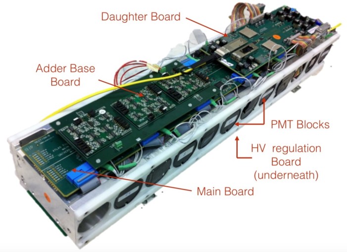
Each mini-drawer forms an independent readout subsystem capable to operate up to 12 PMT channels. A mini-drawer is composed of a mechanical aluminum structure which supports one Mainboard, one Daughterboard, and one high voltage regulation board to read out and operate up to 12 PMT blocks equipped with FENICS front-end boards. The PMT signals are shaped and amplified in two gains by the FENICS, and digitized in the Mainboard by 12-bit dual ADCs. The digitized pulses are transferred to the Daughterboard FPGAs which create and transmit a data packet with the samples to the off-detector electronics through high-speed optical modules.
Figure 3 presents one fully-assembled prototype of a mini-drawer populated with the upgraded on-detector readout electronics and the mechanical aluminum substructure for supporting the PMTs and the electronics.
II-B Off-detector electronics
The off-detector electronics of TileCal for the HL-LHC will be formed by 32 TilePPr modules and 32 TDAQi boards.
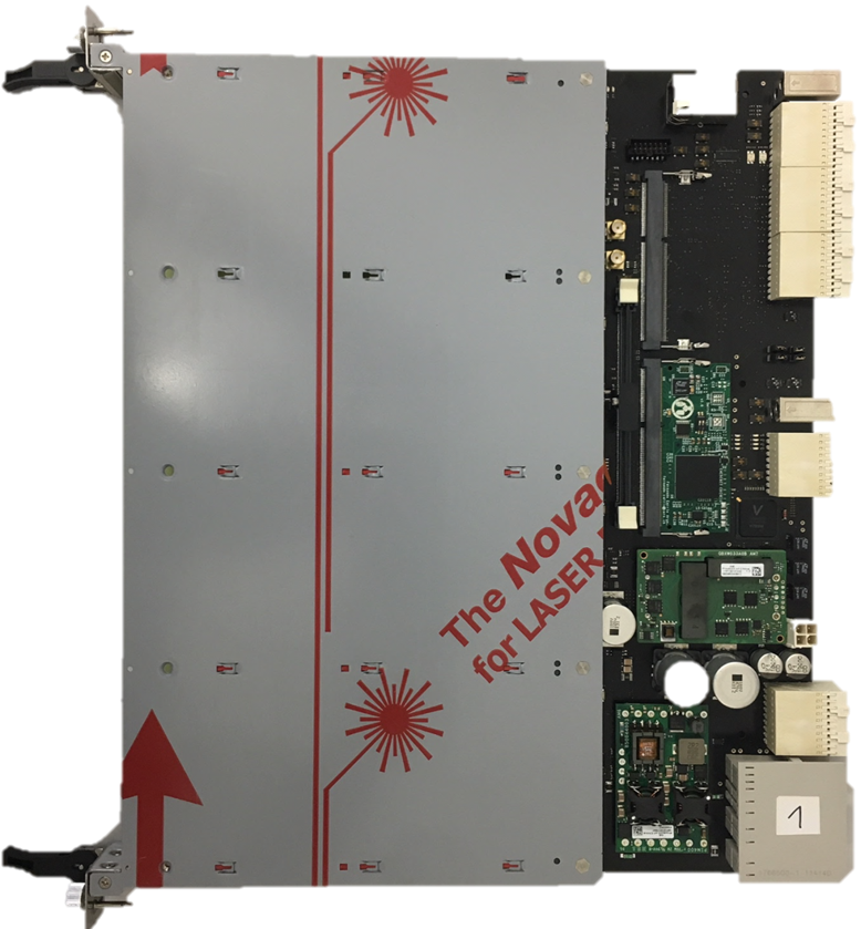
The TilePPr module is composed of an Advanced Telecommunications Computing Architecture (ATCA) [8] Carrier Blade Board (ACBB) and four FPGA-based Compact Processing Modules (CPM).
Figure 4 presents a picture of the ACBB. This board has been designed as an ATCA cutaway carrier board to allow the integration of large heat sinks for the CPMs. The ACBB interconnects the CPMs with the TDAQi system through the Zone 3 connector and provides slow control capabilities through the ATCA infrastructure. The ACBB can deliver up to 400 W at 12 V through the Zone 1 connector.
In order to enhance the maintainability and upgradability of the ACBB during the entire HL-LHC lifetime, the functionalities of the ACBB are implemented into three mezzanine boards:
-
•
The Tile Computer on Module (TileCoM): This board is a System-on-Chip-based board which permits remote configuration and monitoring of the on-detector and off-detector readout systems and interfaces with the Detector Control System (DCS).
-
•
The GbE Switch: This mezzanine provides GbE communication between the CPM, TDAQi and TileCoM boards, and the ATLAS TDAQ system.
-
•
The Intelligent Platform Management Controller (IPMC): The CERN IMPC [9] implements the IPMI (I for Interface) functionalities required for controlling and monitoring the cooling and power system of the ACBB.
III Compact Processing Modules
The Compact Processing Modules are the core processing and high-speed interface of the off-detector electronics of TileCal. The CPMs provide high-speed communication between the on-detector electronics and the ATLAS TDAQ system, where a total of 128 CPMs and 32 ATCA carriers will be required to read out the entire calorimeter in the HL-LHC era.
Each CPM will operate two TileCal modules: one Long Barrel with 45 PMT channels distributed in 4 mini-drawers, and one Extended Barrel with 32 PMTs distributed in 3 mini-drawers.
The optical high-speed interface with the on-detector electronics is implemented via four uplinks (9.6 Gbps) and two downlinks (4.8 Gbps) per mini-drawer using the GigaBit Transceiver (GBT) protocol [10]. The uplinks will transmit 12-bit digitized PMT signals and monitoring data to the CPMs, while the downlinks will provide Detector Control System (DCS) commands and configuration to the on-detector electronics, as well as the bunch-crossing clock for the sampling of the PMT signals.
The energy deposited in each cell is reconstructed and calibrated in real-time from the digitized detector data. The CPM transmits the reconstructed cell energy to the TDAQi per every bunch crossing via four FULL-mode links operating at 9.6 Gbps and using 8b10b encoding [7]. A maximum latency of 1.7 s from the collision time to the reception of the computed trigger objects in the ATLAS trigger system is required to provide enough time to the trigger system for the execution of particle identification and trigger decision algorithms.
Parallel to the trigger path, the Main FPGA of the CPM stores the detector data received from the on-detector electronics and the reconstructed cell energy in RAM block-based pipeline memories, until the reception of a Level-0 trigger acceptance signal. Then, the triggered event data is transmitted to the FELIX system through high-speed links using the FULL-mode protocol for a maximum trigger rate of 1 MHz. In the opposite direction, FELIX provides to the CPMs the Trigger, Timing and Control (TTC) information and bunch-crossing clock via a GBT link at 4.8 Gbps. All high-speed interfaces operate with fixed and deterministic latency.
III-A Hardware design and connectivity
The CPM has been designed as single full-size Advanced Mezzanine Card (AMC) hosting one Xilinx UltraScale FPGA (Main FPGA), one Xilinx Artix FPGA (Control FPGA) and eight Samtec FireFly optical modules. The prototypes of the CPM assembled with the 8 Samtec FireFly modules is presented in Figure 5.
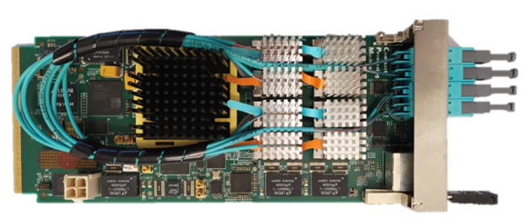
Figure 6 shows a complete block diagram of the CPM and its interconnections. The core processing of the CPM is a Kintex UltraScale FPGA, called Main FPGA. The first CPM prototypes mount a Kintex KU085-1A1517C FPGAs with 48 GTH MultiGigabit Transceivers (MGT) capable of operating up to 12.5 Gbps data rates. The final version of the CPM to be installed in ATLAS will be equipped with a Kintex KU115-1A1517C FPGAs in order to provide a large margin of resources for the implementation of more complex energy reconstruction algorithms.
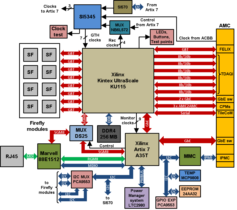
The Main FPGA provides a bidirectional optical communication path with the on-detector electronics via 32 MGTs connected to 8 FireFly modules, while 5 MGTs interface with the TDAQi and FELIX systems through the AMC connector. The remaining MGTs are used for the communication with the GbE Switch and to the other AMCs in the ACBB.
The Modular Management Controller (MMC) of the CPM also communicates through the AMC connector with the IPMC in the carrier to manage the hot swap power sequence and for transmitting health monitoring data.
The slow control and monitoring of the peripherals and power modules relies on a Xilinx XC7A35T-1CSG325C, called Control FPGA. The Control FPGA receives the detector monitoring data from the Main FPGA and transmit it to the ATLAS DCS system through the TileCoM board. Furthermore, the Control FPGA is intended to implement a phase monitoring circuit based on the Digital Dual Mixer Time Difference phase detector [11] for the monitoring of phase variations in the distributed clock with a precision of 30 .
III-B Clocking circuitry
The CPM is responsible for the distribution to the on-detector electronics of the recovered bunch-crossing clock from the FELIX input stream. The designed clock architecture in the CPM permits to extract the recovered clock directly from the MGTs using the dedicated output clock buffers OBUFDS_GTE3 and to clean it with a Si5345 jitter cleaner before routing it back onto the Main FPGA through the transceiver reference clock pins. This clock routing introduces lower levels of jitter than buffering the clock through regular general purpose input/ouput (GPIO) pins to the jitter cleaner [12].
The jitter cleaner outputs six copies of the clean version of the bunch-crossing clock to the MGT banks of the Main FPGA, so that all MGTs can operate using the same reference clock. Additional copies of the bunch-crossing clock are transmitted to the Control FPGA for phase monitoring purposes, and to MMCX connectors to measure the quality of the clock.
The clocking circuitry can be configured to provide three possible clock inputs to the Si5345 jitter cleaner:
-
•
Local programmable oscillator Si570: Used for the initialization of the transceivers and lab tests.
-
•
Recovered clock from FELIX: This clock is buffered through an On Semiconductor NB6LQ572 multiplexer clock. The clock multiplexer permits to choose between different copies of the clock recovered with the MGTs.
-
•
Clock from the ACBB: This clock is intended for lab tests and qualification purposes during the final production of the CPMs.
III-C PCB design
The PCB comprises 14 layers, where 6 are devoted to power distribution and 8 layers are dedicated for high-speed and control signals. The total PCB thickness is 1.6 mm 10%, compliant with the AMC standard. Isola FR408HR was selected as dielectric material due its cost-effective, low dielectric constant ( 3.68) and low loss tangent ( 0.01) compared with other standard FR4 materials.
During the PCB design, signal and power simulations were performed with ANSYS Electromagnetics Suite to verify the signal integrity of the high-speed lines and power planes. Several studies were carried to minimize the insertion loss and impedance discontinuities along the high-speed paths introduced by differential vias and DC-blocking capacitors.
Figure 7 presents the simulation results of the differential insertion loss (SDD21) for the interconnects of the Samtec FireFly module farthest from the Main FPGA. The simulated high-speed interconnects have a maximum length of 7.65 cm.
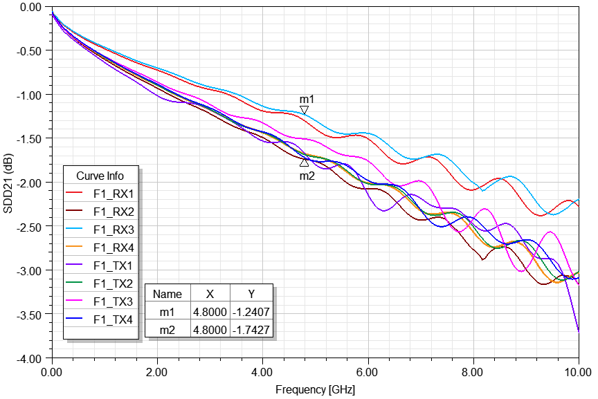
As can be observed in the results, the insertion loss at the Nyquist frequency (4.8 GHz) is between dB and dB, ensuring signal integrity on the high-speed interconnects between the FireFly modules and the Main FPGA.
IV Test and Verification
This section presents the test results obtained during the verification of the first CPM prototypes. These tests included the qualification of the high-speed links to the on-detector electronics and the clock distribution capabilities of the CPM.
IV-A Link qualification tests
The 32 optical links connected to the Main FPGA have been qualified with the Xilinx IBERT IP core [13] through Bit Error Rate (BER) tests running the links at 9.6 Gbps.
The setup consisted in two separated CPMs transmitting and receiving Pseudo-Random Bit Sequence (PRBS31) data patterns during seven days. No errors were found in any link providing a BER better than per link with a Confidence Level (CL) of 95 %, and a total combined BER better than with a CL of 95 %.
Furthermore, the power consumption during the test was about 32 W. The CPM consumption during operation is expected to increase by 12 W due to additional firmware. This estimation was obtained from the Xilinx Power Estimator tool and the expected resource use for the final firmware. These preliminary estimations predict that the power consumption of the CPM will be within the power consumption budget of 60 W per AMC specified by the ATCA standard [8].
IV-B Signal integrity validation
As part of the validation tests of the CPMs, the eye diagrams were measured at the output of the Samtec FireFly modules using a DCA-X 86100D sampling oscilloscope from Keysight. The measurements were done transmitting a PRBS31 data pattern at data rates of 4.8 Gbps and 9.6 Gbps.
Figure 8 shows the results of the eye diagram measurements for 4.8 Gbps (a) and for 9.6 Gbps (b). In both cases, the eye diagrams are widely opened without signs of excessive jitter, presenting satisfactory noise margins.
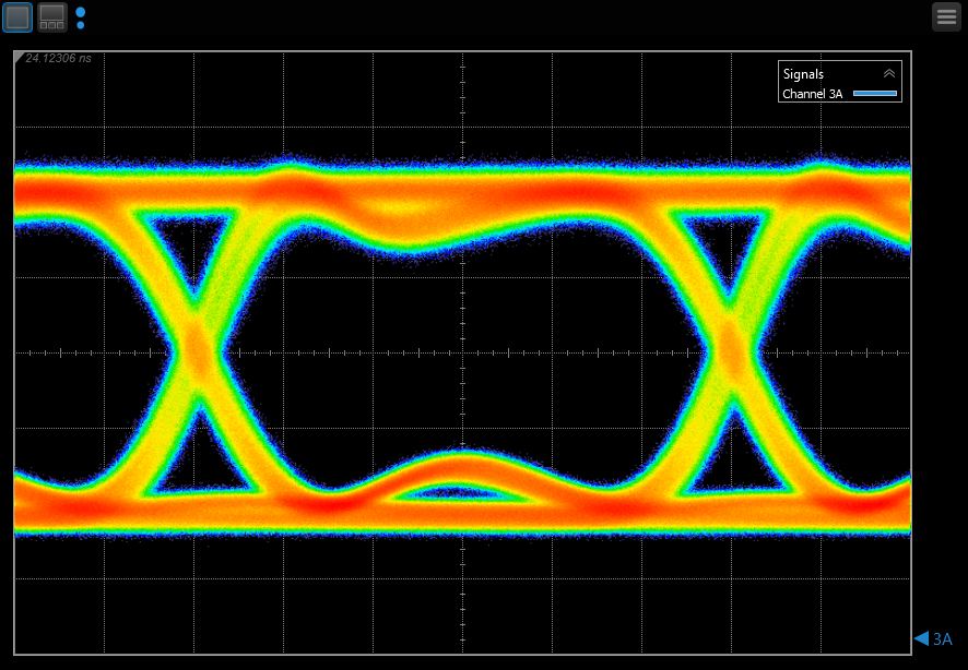
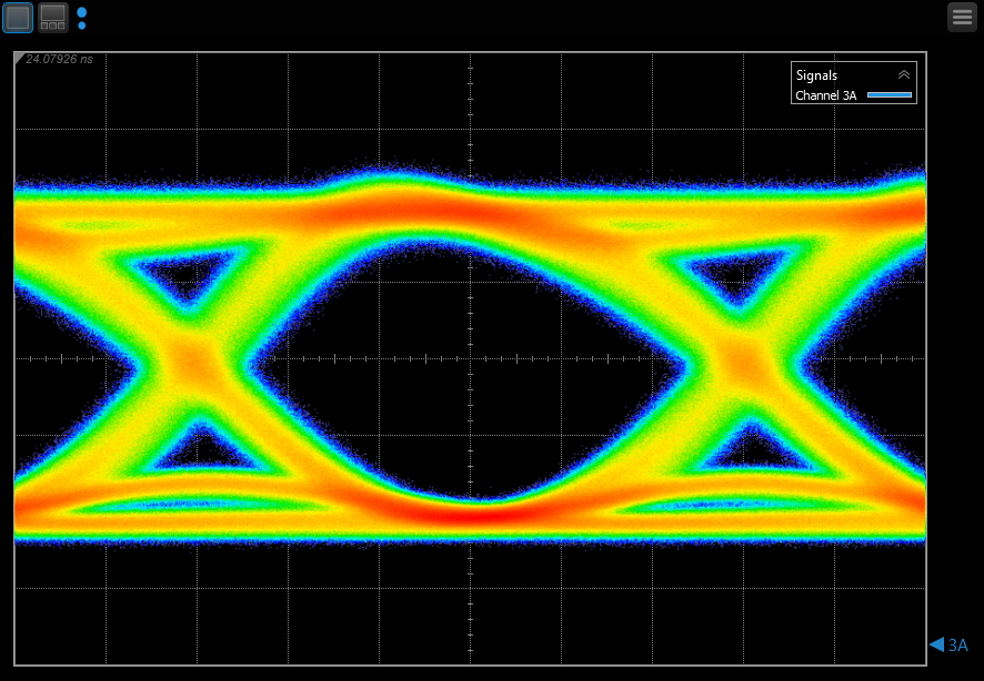
Signal quality parameters were extracted from the eye diagram data as part of the validation tests. Table I summarizes the extracted jitter values, eye height and width.
| Parameter | 4.8 Gbps | 9.6 Gbps |
|---|---|---|
| Eye Width | 191.84 ps | 85.92 ps |
| Eye Height | 73.15% | 87.10% |
| RJ (rms) | 1.94 ps | 1.84 ps |
| DJ (-) | 2.40 ps | 5.85 ps |
| TJ () | 28.84 ps | 30.96 ps |
| TJ () | 30.09 ps | 32.15 ps |
| TJ () | 31.30 ps | 33.28 ps |
| TJ () | 32.45 ps | 34.38 ps |
| TJ () | 33.56 ps | 34.43 ps |
The signal quality at the input of the CPM was also studied using the built-in capabilities of the Xilinx transceivers. For these measurements, the same setup presented in section IV-A is used. The receiver of the MGTs includes a second independent sampler after the equalizer which runs in parallel with the Clock and Data Recovery (CDR) data sampler. The results from both samplers are compared to perform the BER tests and to compose eye diagrams.
Figure 9 presents the eye diagram at the input of the FPGA for a BER better than per sampling point and a data rate of 9.6 Gbps. The eye diagram is scanned across vertically and horizontally by controlling the clock phase of the sampler and the offset voltage.
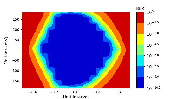
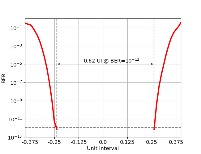
An horizontal BER test scan was performed by shifting the phase clock of the second sampler horizontally across the eye, and setting the voltage offset to the center of the eye.
The resulting BER curve is a bathtub curve, so-called because of its characteristic shape, shown in Figure 10. The BER is below at the center of the eye and increases when getting closer to the eye crossings.
The distance between the left and the right curves defines a noise margin of 0.62 Unit Interval (64.58 ps) at the specified BER level of . All channels were verified and validated showing similar quantities.
IV-C Clock qualification tests
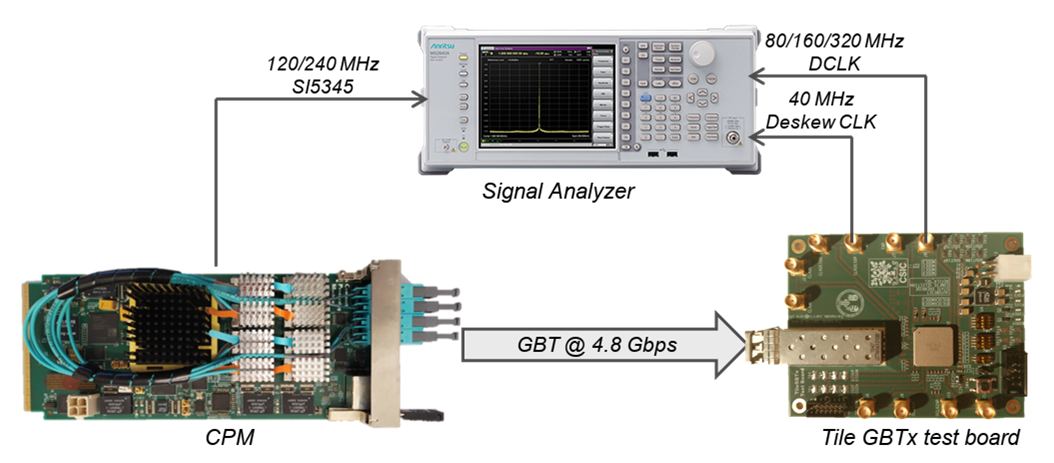
In order to study the performance of the clock distribution system, phase noise measurements were carried with a MS2840A signal analyzer from Anritsu at room temperature. Figure 11 presents a block diagram of the setup for the clock qualification tests. The setup consisted in a CPM with a GBT link transmitting at 4.8 Gbps to a GBTx chip [14] in a test board via a SFP module.
The GBTx chip is a 130 nm CMOS rad-hard device intended for high-speed communications and slow control in High Energy Physics experiments. This chip is able to recover the bunch-crossing clock from the input serial link providing up to 8 independent output clocks with programmable phase and up to 40 clocks with a fixed phase. Both types of clocks can be configured to buffer 40, 80, 160 and 320 MHz clocks.
However, the phase-programmable clocks present higher levels of random jitter than the e-link clocks, showing a phase noise peak around 1 MHz introduced by the internal delay lines used for shifting the phase. For this reason, the e-link clock is preferred over the Phase-Shift clock (PS clock) as reference clock for driving the MGTs of the Daughterboard FPGAs. Despite its higher jitter, the PS clock is used as input clock to the Mainboard ADCs since the phase-tuning capability is desirable to minimize the error of the real time energy reconstruction algorithms and for pulse characterization purposes and calibration.
Figure 12 presents the measured phase noise plot of the e-link and PS clocks for different frequencies, as well as the corresponding phase noise mask provided by the FPGA manufacturer to ensure minimal jitter in the MGT outputs [15]. In this test, the clock source was the on-board Si5345 jitter cleaner driven by the on-board Si570 oscillator.
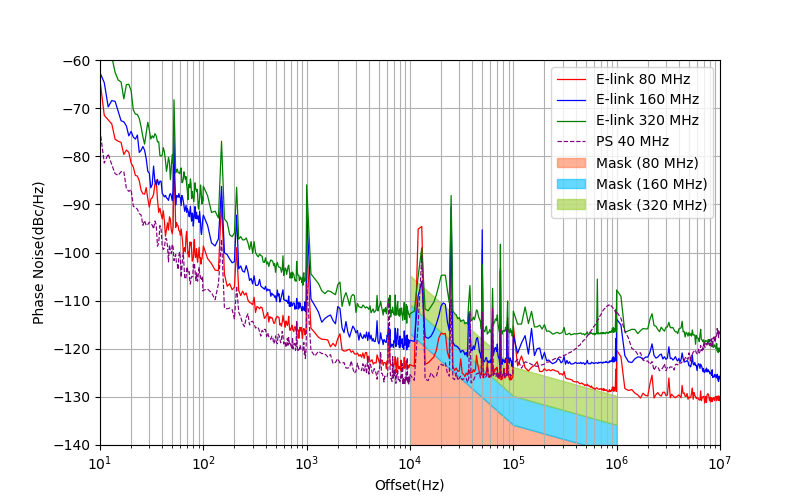
The e-links were configured to provide recovered clocks with frequencies of 80 MHz, 160 MHz and 320 MHz. The phase noise of the 40 MHz e-link clock is not shown for simplicity, since 40 MHz is outside the frequency range for the reference clock of the MGTs. Similarly, only the phase noise of the 40 MHz PS clock is presented because it is the only possible input clock frequency for the 12-bit ADCs on the Mainboard.
As observed in Figure 12, the phase noise values of all the e-link clocks exceeds the phase noise limits for the reference clocks addressed by the FPGA manufacturer. However, stable communication between the CPM and the Daughterboard v5 [16] is achieved using the GBT protocol at 4.8 Gbps for the downlink and 9.6 Gbps for the uplink.
Table II shows the integrated RMS jitter extracted from the phase noise measurements of the two types GBTx output clocks and for all frequencies. The RMS jitter was obtained integrating the phase noise response over the entire bandwidth (from 10 Hz to 10 MHz) and over the sensitive bandwidth of the MGT (from 10 kHz to 1 MHz).
| Reference | 10 Hz–10 MHz | 10 kHz–1 MHz |
|---|---|---|
| E-link 40 MHz | 6.43 ps | 3.60 ps |
| E-link 80 MHz | 4.57 ps | 2.91 ps |
| E-link 160 MHz | 3.96 ps | 1.75 ps |
| E-link 320 MHz | 4.02 ps | 1.43 ps |
| PS 40 MHz | 20.10 ps | 9.88 ps |
| PS 80 MHz | 12.81 ps | 9.78 ps |
| PS 160 MHz | 12.21 ps | 9.57 ps |
| PS 320 MHz | 12.23 ps | 9.66 ps |
The RMS jitter of the 80/160/320 MHz PS clocks for the entire bandwidth is about three times higher than in the e-link clocks. In the frequency range specified by the manufacturer, the RMS jitter is up to seven times higher in the PS clocks.
Finally, the phase noise at the outputs of the Si5345 jitter cleaner of the CPM was measured. Two different clock frequencies of 120 MHz and 240 MHz were considered as reference clocks for the implementation of the GBT protocol.
Figure 13 shows the phase noise measurements for the two reference clocks in the CPM and the corresponding phase noise masks.
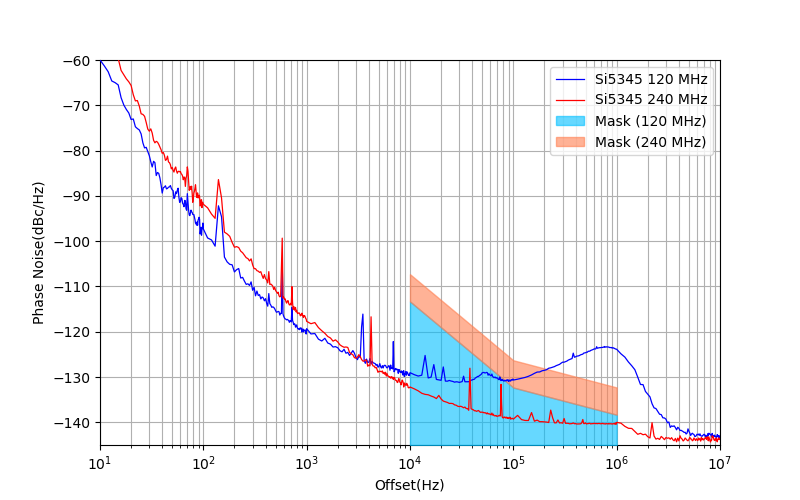
As observed in Figure 13 and Table III, the phase noise for the 120 MHz clock is higher than for the 240 MHz clock in the range of frequencies from 10 kHz to 1 MHz, exceeding the manufacturer specifications. However, the tests reveled that the configuration of the Si5345 chip did not cause any relevant effect on the phase noise of the recovered clock indicating that the main jitter contribution is dominated by the CDR of the GBTx.
| Reference | 10 Hz–10 MHz | 10 kHz–1 MHz |
|---|---|---|
| Si5345 120 MHz | 3.75 ps | 1.04 ps |
| Si5345 240 MHz | 3.57 ps | 0.10 ps |
V Conclusions and Future Plans
The new conditions of the HL-LHC implies a complete replacement of the on- and off- detector electronics of the Tile Calorimeter. In addition, a new readout and clocking architecture is needed to fulfill the requirements of the fully digital trigger for the ATLAS Phase-II Upgrade.
The Compact Processing Modules will be the core processing unit of the Tile off-detector electronics at the HL-LHC. The CPMs will interface between the on-detector electronics and the ATLAS TDAQ system, reading out and controlling the on-detector electronics and providing reconstructed cell energy to the ATLAS trigger system in real time.
The first prototypes of the Compact Processing Module for the HL-LHC have been produced and validated. All interfaces have been validated and qualified with BER tests and measuring the optical eye diagrams. Phase noise measurements of the bunch-crossing clock at the CPM present low noise levels which comply with the FPGA manufacturer specifications. The distributed bunch-crossing clock at the test board shows larger phase noise values dominated by the CDR of the GBTx.
Following the ATLAS installation plans for 2025, the production of the CPMs will be divided in two stages: a pre-production of 14 CPMs scheduled for the third quarter of 2021, and a final production of 114 CPM planned by the last quarter of 2023. The complete readout system will be installed in the ATLAS counting rooms in September 2025.
References
- [1] ATLAS Collaboration. The ATLAS Experiment at the CERN Large Hadron Collider. Journal of Instrumentation, 3:S08003, 2008.
- [2] ATLAS Collaboration. Readiness of the ATLAS Tile Calorimeter for LHC collisions. Eur. Phys. J., C70:1193–1236, 2010.
- [3] A. Valero et al. ATLAS TileCal Read Out Driver production. Journal of Instrumentation, 2:P05003, 2007.
- [4] ATLAS Collaboration. Technical Design Report for the Phase-II Upgrade of the ATLAS Tile Calorimeter. Technical Report CERN-LHCC-2017-019. ATLAS-TDR-028, CERN, 2017.
- [5] F. Carrió and A. Valero. The PreProcessor module for the ATLAS Tile Calorimeter at the HL-LHC. Nucl. Instrum. Methods Phys. Res., A, 958:162487, 2020.
- [6] ATLAS Collaboration. Technical Design Report for the Phase-II Upgrade of the ATLAS TDAQ System. Technical Report CERN-LHCC-2017-020. ATLAS-TDR-029, CERN, 2017.
- [7] J. Anderson et al. FELIX: a High-Throughput Network Approach for Interfacing to Front End Electronics for ATLAS Upgrades. J. Phys. Conf. Ser., 664(8):082050, 2015.
- [8] PICMG. AdvancedTCA Short Form Specification, technical report, January 2003.
- [9] J.M. Mendez, V. Bobillier, S.L. Haas, M. Joos, S. Mico, and F. Vasey. CERN-IPMC solution for AdvancedTCA blades. PoS, TWEPP-17:053, 2018.
- [10] M. Barros Marin, S. Baron, S.S. Feger, P. Leitao, E.S. Lupu, C. Soos, P. Vichoudis, and K. Wyllie. The GBT-FPGA core: features and challenges. Journal of Instrumentation, 10(03):C03021–C03021, mar 2015.
- [11] F. Carrió and A. Valero. Clock Distribution and Readout Architecture for the ATLAS Tile Calorimeter at the HL-LHC. IEEE Transactions on Nuclear Science, 66(7):1014–1020, 2019.
- [12] E. Mendes, S. Baron, C. Soos, J. Troska, and P. Novellini. Achieving Picosecond-Level Phase Stability in Timing Distribution Systems With Xilinx Ultrascale Transceivers. IEEE Transactions on Nuclear Science, 67(3):473–481, 2020.
- [13] Xilinx Inc. IBERT for UltraScale GTH Transceivers v1.4 - PG173, June 2018.
- [14] P. Leitao, S. Feger, D. Porret, S. Baron, K. Wyllie, M. Barros Marin, D. Figueiredo, R. Francisco, J.C. Da Silva, T. Grassi, and P. Moreira. Test bench development for the radiation hard GBTX ASIC. Journal of Instrumentation, 10(01):C01038–C01038, jan 2015.
- [15] Xilinx Inc. Kintex UltraScale FPGAs Data Sheet:DC and AC Switching Characteristics - DS892 (v.1.19), September 2020.
- [16] E. Valdes Santurio, S. Silverstein, and C. Bohm. Readiness of the ATLAS Tile Calorimeter link daughterboard for the High Luminosity LHC era. PoS, TWEPP2019:087, 2020.