Creation and annihilation of mobile fractional solitons in atomic chains
Abstract
Localized modes in one dimensional topological systems, such as Majonara modes in topological superconductors, are promising platforms for robust information processing. In one dimensional topological insulators, mobile topological solitons are expected but have not been fully realized yet. We discover fractionalized phase defects moving along trimer silicon atomic chains formed along step edges of a vicinal silicon surface. Tunneling microscopy identifies local defects with phase shifts of 2/3 and 4/3 with their electronic states within the band gap and with their motions activated above 100 K. Theoretical calculations reveal the topological soliton origin of the phase defects with fractional charges of 2/3 and 4/3. An individual soliton can be created and annihilated at a desired location by current pulse from the probe tip. Mobile and manipulatable topological solitons discovered here provide a new platform of robustly-protected informatics with extraordinary functionalities.
INTRODUCTION
Localized topological modes, such as Majorana edge modes in topological superconductors dego13 ; lin17 and skyrmion excitations in magnetic materials fert17 ; chac18 , are attracting great interest as promising platforms for robust information processing hasa10 ; qi11 . For one dimensional (1D) topological insulators, another kind of topological local modes, solitons su79 ; su80 ; heeg88 ; hern20 , has been known for a long time. Topological solitons, which have both edge-mode and excitation characteristics, have been identified not only in spontaneous 1D insulators such as polyacetylene chains heeg88 and surface atomic chains cheo15 but also in ultracold atoms atal13 ; he18 ; lchen18 , photonic crystals krau12 ; verb13 ; posh15 , and acoustic lattices xiao15 ; yang16 . In contrast to a Majonara edge mode, solitons can move fast with topologically protected information as in the case of an unpinned skyrmion. The technology of using solitons as the robust media of delivering information was well established in classical wave systems based on optical solitons zyss98 ; ouzo03 . In quantum mechanical systems, solitons can provide even more exciting opportunities such as the multilevel information processing hata97 ; akhm00 , quantum entanglements szum15 ; pend20 , and the utilization of fractional quanta su81 ; schr81 ; rice82 . Among these exciting possibilities, only the multilevel information processing has been demonstrated recently by the solitons in indium atomic chains kim17 . However, the soliton motion is largely prohibited by pinning defects or the interchain interaction in most 1D electronic systems kim17 ; lee19 , making the realization of a mobile soliton with fractionalized quanta and quantum information a long-standing challenge. Beyond observing the existence and the interaction of solitons, the generation and manipulation of individual solitons in electronic systems has to be demonstrated for many possible applications.
Among various proposals in these challenges su81 ; schr81 ; rice82 , the trimer chains have been the most widely discussed with a particular focus on fractional charges. In 1D electronic systems of trimers, solitons are endowed with fractional charges of 2/3 and 4/3 in contrast to integer charges of solitons in conventional dimer chains due to the spin degree of freedom su79 ; su80 . That is, trimer solitons are the simplest form of fractionalized solitons in an electronic system. Contrary to the simplicity, theoretical works reveal various exotic properties of solitons in trimer systems dros17 ; jin17 ; liu17 ; mart19 ; conz20 . Moreover, considering the well established ternary computing architecture conn08 and the current interest in the ternary system for low power and/or neuromorphic computing systems jeon19 , the utilization of topologically protected trimer solitons is expected to expedite exciting development in information technology. However, no electronic system with trimer solitons has been identified yet.
In this respect, the silicon atomic chains on a vicinally-cut silicon crystal [Si(553)] has attracted our attention. By adsorption of a proper amount of gold atoms, a regular array of step-edge silicon chains is stabilized with unsaturated dangling bonds. This system was found to transit into a trimer structure below about 200 K ahn05 ; snij06 ; brau18 and the existence of the phase defects were noticed with their mobility and topological nature unknown snij06 ; shin12 ; hafk20 . In the present work, we directly identify individual mobile solitons along these trimer atomic chains by scanning tunneling microscopy and spectroscopy (STM/S). Two different types of solitons with fractionalized (2/3 and 4/3) phase shifts, respectively, are observed, which are immobile at low temperature but their motion turns on above 100 K. Their solitonic property is unambiguously confirmed by their in-gap electronic states and their immunity for scattering. Density functional theory (DFT) and tight-binding calculations reveal further the topological properties of these solitons and their fractionalized charges. This is the first direct microscopic observation of a mobile soliton and a trimer soliton in an electronic system. We also succeed to generate and annihilate a soliton on a desired location by the tunneling electron pulse from the probe tip, making the first step toward the manipulation of individual solitons. An avenue toward exploiting mobile and robust carriers of fractional quanta is thus widely opened.
RESULTS
Direct observation of mobile phase defects
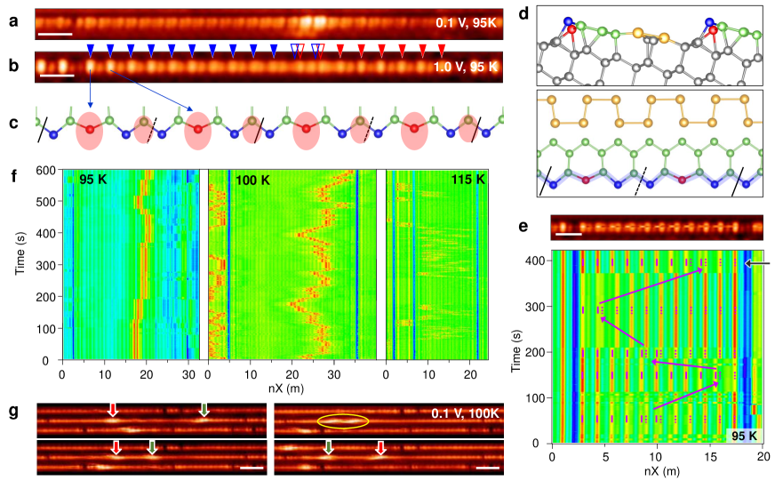
The surface of a vicinal Si(553) crystal with an optimized coverage of Au adatoms form a well ordered array of Si and Au atomic chains with very narrow (1.3 nm in width) terraces (Fig. 1g) erwi10 ; aulb13 ; brau18 . Each terrace consists basically of double Au chains and a Si honeycomb chain on its topmost layer (Fig. 1d) erwi10 ; aulb13 ; brau18 (more detailed atomic structure in Supplementary Fig. 6). What concern the present work are step-edge Si atoms with dangling bonds, which correspond to one side of the Si honeycomb chain (blue and red balls in Fig. 1c) and to the rows of bright protrusions in the STM topographs (Fig. 1b). Its low-temperature atomic structure has long been intrigued with contradictory suggestions of a CDW insulator with a periodic lattice distortion ahn05 ; snij06 and an antiferromagnetic insulator with a spin ordering erwi10 . Very recent DFT calculations successfully found a distorted CDW structure explaining most of the experimental data brau18 . Below the transition temperature of 200 K, the STM images exhibit a structural distortion in a high empty-state bias, namely, the alternation of bright and dim protrusions in a 3a0 (a0, silicon surface unit cell of 0.384 nm) periodicity (Fig. 1b), which represent a monomer and a dimer in each trimer unit cell, respectively. As detailed below, this distorted structure is a 1D CDW state as driven by the quasi 1D metallic band of unsaturated dangling bonds of step-edge Si atoms (Fig. 2a).
The silicon trimer chains are well known to contain extrinsic defects, which appear as missing bright protrusions in high bias STM images snij06 ; shin12 . However, extra local features appear with bright contrast when we lower the bias closer to the Fermi energy where the 3a0 periodic modulation in STM becomes weak (Fig. 1a). A careful inspection of this extra feature back in the high bias image reveals the presence of a phase mismatch of the 3a0 periodicity such as a 4 (4a0) or a 5 (5a0) (2 (2a0)) unit with gradually decreasing amplitude of the 3a0 protrusions (Fig. 1b and Supplementary Fig. 2). Moreover, the hopping of the phase defect is frequently noticed by the sudden a0 shift of the 3a0 modulations (Figs. 1e and 1f) and its motion is even directly imaged in sequential STM images (Fig. 1g and Supplementary Movie 1). The enhanced contrast of the phase defects in the low bias suggests the existence of a localized in-gap state. These observations indicate that the trimer Si chains have mobile topological solitons emerging from its 1D CDW states as revealed unambiguously below. Note that the previous observations of the phase defects snij06 ; shin12 ; hafk20 had no means to reveal their intrinsic soliton nature.
Electronic structure of Si atomic chains
The undistorted Si step-edge chain has a strongly-1D and partially-filled electronic band due to its dangling bond electrons (Supplementary Fig. 8a). In the present structure model, fully relaxed within the DFT calculations (Fig. 1d) brau18 , every third Si atom along the step edge is distorted downward to split the band with an energy gap of 0.6 eV at the Fermi level (Fig. 2a). The band gap is due to the rehybridization of dangling bonds into and orbitals; the unoccupied bands around 0.2 eV from distorted Si atoms (red balls in Fig. 1d) and the occupied bands around -0.4 and -0.7 eV from undistorted Si atoms (blue balls). This electronic structure is consistent with the spectroscopy observation shown in Fig. 3d.
This band structure can be described well with a much simpler 1D tight-binding model considering only the single Si zigzag chain at the step edge (yellow lines in Fig. 2a). The neighboring Au chains (the bands of dashed lines) affect only the fine structures of the valence bands around -0.4 -0.7 eV, which do not affect the following discussion (Supplementary Fig. 11). This 1D tight binding model is straightforwardly transformed into a trimer Su-Schrieffer-Heeger (SSH) Hamiltonian as described by three hopping amplitudes (Fig. 2b); t1 of 0.57 eV, as enhanced by the shorter Si-Si bond length due to the trimer distortion, and the t2 and t3 of 0.47 and 0.43 eV, respectively.
Atomic and electronic structures of mobile phase defects
Breaking translational symmetry by the trimer structure immediately leads to three degenerated ground states with fractionalized phase shifts of 0, 2/3, and 4/3 (Fig. 2b). These ground states can be connected with a few different types of phase defects (or domain walls) as shown in Fig. 2c and Supplementary Fig. 7. Only four of them are distinct, which we label with the distance between the neighboring Si atoms distorted. Namely, a defect with a phase shift of 2/3 (4/3) corresponds to the 2 (2a0) or 5 (1 or 4) defects. In order to identify detailed atomic and electronic structures of them, we performed DFT calculations with huge supercells (Supplementary Fig. 3). The results reveal that the 4 structure is most stable in energetics [the formation energy of 0.092 (4), 0.124 (5), and 0.177 (2) eV/unit cell] (Supplementary Table I). The simulated STM image for the 4 structure reproduces fairly well the experimental ones discussed above, that is, the enhanced contrast at 0.1 V and the shifted protrusions at 1.0 V (Fig. 3a). We also examined the other structure model proposed for the present system, the antiferromagnetic chain model erwi10 , but the phase defects could not be reproduced consistently (Supplementary Fig. 5).
The DFT (and also the tight-binding) calculations predict that the 4 phase defect has its own electronic states within the band gap of the trimer chain as shown in Fig 3c. The empty and filled states of the pristine 3a0 Si chain are located at about +0.3 and -0.5 eV but the phase defect has its localized electronic state at around -0.2 eV. The localized in-gap state is clearly visualized in the STS map on a 4 phase defect (Fig. 3c). The phase shifts, atomic structures, and the in-gap electronic states detailed above converge convincingly to the topological soliton picture of the phase defects observed.
Among four different types of phase defects (Fig. 2c), the 4 defect was found to be most popular (Supplementary Fig. 1) in accord to the energetics calculated. The 1 defect is unstable to relax spontaneously into the 4 defect. The 2 defect can also easily relax into the 5 defect by simply recovering one distorted Si atom as shown in Fig. 2c. The energy barrier of this process is as small as 0.01 eV (Supplementary Fig. 15). Even the 5 defect can transform into a more energetically favorable structure of two 4 defects combined (called as 44) as shown in Fig. 2d. The energy barrier is 0.06 eV being smaller than the hopping barrier of about 0.1 eV (Supplementary Fig. 15).
Indeed, we find quite a few 44 defect but rarely a 5 defect (Supplementary Fig. 1). Note that the phase shifts themselves are preserved in these relaxation processes of the phase defects. The simulated STM image (Fig. 2f) of a 44 defect or a two soliton bound state is in good agreement with the experiment. Its electronic structure is similar to the isolated 4 defect in both experiments and calculations (Supplementary Fig. 4) except for a small bonding-antibonding splitting (Supplementary Fig. 3). The merging and splitting of two 4 defects are hinted in the real time imaging (Fig. 1g and the supplementary movie1).
Topological nature and fractional charges
As any other topological system, the topological nature of the present system is revealed by analyzing its band structure and edge states. The topological invariant of a trimer chain can be related to an effective higher dimensional (2D) bulk system theoretically krau12 . We construct such a 2D model by putting an adiabatic dimension and obtain the Chern numbers of (-1, 2, -1) for the three lowest energy bands (Supplementary Fig. 10) as predicted in previous theoretical studies mart19 ; ke16 . The band gaps of the system contain five different edge states dictated by the topology (Fig. 2e), which match well the DFT calculations (Supplementary Fig. 9). The major edge state of the C phase around 0.2 eV corresponds to the in-gap state observed in the experiment. A 2/3 or 4/3 fractional phase shift for an 1D electronic system guarantees fractionalized charges on corresponding solitons, while measuring the charge itself is a tremendous technical challenge - the tunneling occurs through not solitons themselves but electrons. In theoretical aspects, we found that the 4/3 phase-shift soliton has the fractionalized charges of +2e/3 (occupied) and -e/3 (empty) per spin and the 2/3 phase-shift soliton has +e/3 (occupied) and -2e/3 (empty) per spin (Supplementary Fig. 12 and 13) conz20 . The fractional charge is insensitive to detailed domain wall structures but depends only on the phase shift due to its topological origin. For example, the fractional charge on a 5 and a 44 defects is consistent (Supplementary Fig. 13).
Soliton motions
We observe that the phase defects propagate at a higher temperature. At a 90 K, one seldom see the hopping of solitons, but, at 95 K, they exhibit several hoppings (by one 3a0 unit cell of 1.16 nm) within a time window of 600 sec (Fig. 1e and 1f). The hopping becomes more and more frequent with only a small change of the temperature as shown in Fig. 1f (Supplementary Movie1) and solitons become highly mobile already at 115 K. The drift velocity of the soliton at 100 K is measured as 0.10 nm/sec, which increase to 0.65 nm/sec at 115 K (Supplementary Fig. 14). An estimation of Arrhenius-type diffusion velocity, D=D0exp(-Eb/T), gives the expectation of the velocity enhancement of 4.28 from 100 to 115 K (Supplementary Fig. 15a), which is roughly consistent with the observation. The turn-on of the soliton motion at around 100 K, related to the hopping barrier of a soliton 0.1 eV (Supplementary Fig. 15), seems consistent with the thermally induced disordering of the 3a0 lattice, which was attributed to the generation of phase defects hafk20 . The real time images also clearly indicate that the soliton is immune to the defect scattering (it bounces back or jumps over the extrinsic defects, Fig. 1f) and the soliton-soliton scattering (they are reflected but prohibited to pass through, Fig. 1g, and Supplementary Movie1, and Supplementary Fig. 16). Of course, when the ground state structure of the Si chain is destroyed, for example, by impurity adsorption and increase of temperature, its edge modes, solitons, cannot be sustained.
Generation of a single soliton
A soliton is found to be reproducibly generated under the probe tip by the tunneling bias application at very low temperature. Figure 4a shows an atomically resolved atomic force microscopy (AFM) image of the surface at 4.4 K. In the AFM image, two undistorted Si atoms (blue atoms in the model of Fig. 2) of a trimer appear as dark contrast due to their closer distance to the tip. After the application of a single tunneling pulse at the location of the distorted Si atom (yellow circled in Fig. 4a), one can observe one trimer destroyed (Fig. 4b). This transiently forms a 6 chain in our structure model (Fig. 2) and relaxes into a 5 soliton (Fig. 4c) and the phase shift of the neighboring trimers. This indicates the pair creation of 1 and 5 solitons with the former quickly moving out of the view frame to induce the phase shift. The soliton can also be erased by applying the same bias in a nearby site as shown in Figs. 4d-4f. That is, the second soliton generated annihilates the first one. This switches back-and-forth the topological phase shift of a given trimer chain as shown in Figs. 4d-4f. That is, one can manipulate a single soliton and decode the topological phase information on each chain.
Discussion
A material realization of a fractionalized soliton has been elusive in an electronic system. Note that the popular dimer solitons has no electronic fractionalization due to the spin degeneracy. A close electronic example available is the phase defects in finite size artificial lattices based on a 2D surface state and adsorbates huda20 . However, this system only provides the static modulation of hopping amplitudes for an electronic orbital well away from the Fermi level to preclude the motion and the charge fractionalization. That is, these phase defects do not feature the dynamic nature, which is essential to a soliton.
The high mobility of the soliton observed directly here is notable since most of the solitons in previous works on solid surfaces are strongly pinned by defects or the strong interchain interaction lee19 . Mobile fractional solitons are contrasted with Majorana edge modes, for which an isolated mobile form has not been identified yet. The present solitons are further contrasted with Majorana modes and skyrmions by the fractionalized quanta associated. The soliton-soliton interaction glimpsed here as the formation of a soliton pair has an important implication in quantum information processing to secure an entangled state of solitons cold10 ; krup17 ; szum15 ; pend20 . The demonstration of the reproducible creation of an individual soliton here would open the door toward the manipulation of such information. Most of the essential ingredients for the exploitation of technological potentials of solitons in electronic systems are secured, such as the high mobility, the artificial generation/annihilation, the switchability kim17 , and the mutual interaction.
METHODS
Sample preparations. The Si(553)-Au surface with a regular array of alternating Au chains and Si step-edge chains was fabricated by depositing Au of about 0.5 monolayer using a thermal evaporator onto a well cleaned Si(553) substrate at a temperature of 920 K in ultra high vacuum. The Si(553) substrate was cleaned by repeated flash heatings at 1500 K. The well ordered array was confirmed by low-energy-electron diffraction and STM images.
STM measurements. The STM measurements were performed using a commercial low temperature STM apparatus in a ultra high vacuum chamber. The system was cooled down by liquid nitrogen while the temperature was carefully controlled by a built-in resistive heater. The measurement was done at various different temperatures between 78 and 125 K at various different biases. The tunneling current was typically fixed at 30 pA. The STS (dI/dV) measurement was performed using the standard lock-in technique with a lock-in modulation of 20 mV at 910 Hz and a tunneling current of 200 pA. For time-dependent topographic measurements for a short segment of a wire, the time resolution between successive scans is about a few sec.
AFM measurements. The imaging of the surface structure manipulation was performed by high-resolution noncontact atomic force microscopy (nc-AFM) and scanning tunneling microscopy (STM) under ultra high vacuum at 4.3 K using a commercial low temperature microscope (SPECS GmbH) with the simultaneous force-current detection capability. This combined system can effectively decouple the excitation source (tunneling current) and the local structural probe (AFM) so that the surface structure was investigated precisely by frequency shift () images while the tunneling current was limited to generate transient structures. The images were recorded at constant height. In the noncontact regime, increases in negative direction as the tip-sample distance gets closer, which means a more protruding structure appears darker.
Structure manipulation. Step-edge Si trimer chains can be shifted reproducibly by exciting a local transient structure with the tunneling current injected. The local transient structure was generated using a bias pulse of +0.15 V on top of the trimer center at 4.3 K. After the sufficient time elapsed, the equilibrium state was achieved by the propagation of the soliton structure along the chain, which led to the phase shift in the trimer structure. We found that the initial excitation site, a trimer center, is prohibited from returning back to the sane trimer center, which forces a 1 lateral shift of the original trimer structure. At a higher temperature than 4.3 K, a higher voltage is expected to induce the locally excited structure or solitons.
DFT calculations. DFT calculations were performed by using the Vienna simulation package kres96 within the generalized-gradient approximation (GGA) using the revised Perdew-Burke-Ernzerhof (PBEsol) functional perd08 . The Si(553)-Au surface is modeled within periodic supercells with at least four bulklike Si layers and a vacuum spacing of about 12.8 Å. The bottom of the slab is passivated by H atom. We used a plane-wave basis with a kinetic energy cutoff of 312 eV and a 521 -point mesh for the clean Si(553)-Au surface. All atoms but the bottom two Si layers held fixed at the bulk positions are relaxed until the residual force components were within 0.03 eV/Å. We employed large supercells for the defects (14 17a0) and their energetics is summarized in Supplementary Table I. It shows that its relative stability is sound, even though it is difficult to obtain the well-converged isolated energy of solitons due to huge and different sized supercells. For the tight-binding model calculations, we used the PythTb package by Coh and Vanderbilt pythTB .
References
- (1) W. DeGottardi, D. Sen, and S. Vishveshwara, Majorana fermions in superconducting 1D systems having periodic, quasiperiodic, and disordered potentials, Phys. Rev. Lett. 110, 146404 (2013).
- (2) Y. Lin, W. Hao, M. Wang, J. Qian, H. Guo, Topological superconductors from one-dimensional periodically modulated Majorana chains, Sci. Rep. 7, 9210 (2017).
- (3) A. Fert, N. Reyren, and V. Cros, Magnetic skyrmions: advanceds in physics and potential applications, Nat. Rev. Mater. 2, 17031 (2017).
- (4) A. Chacon, L. Heinen, M. Halder, A. Bauer, W. Simeth, S. Mühlbauer, H. Berger, M. Garst, A. Rosch, and C. Pfleiderer, Observation of two independent skyrmion phases in a chiral magnetic material, Nat. Phys. 14, 936 (2018).
- (5) M. Z. Hasan and C. L. Kane, Colloquium: Topological insulators, Rev. Mod. Phys. 82, 3045 (2010).
- (6) X.-L. Qi and S.-C. Zhang, Topological insulators and superconductors, Rev. Mod. Phys. 83, 1057 (2011).
- (7) W. P. Su, J. R. Schrieffer, and A. J. Heeger, Solitons in polyacetylene, Phys. Rev. Lett. 42, 1698 (1979).
- (8) W. P. Su, J. R. Schrieffer, and A. J. Heeger, Soliton excitations in polyacetylene, Phys. Rev. B 22, 2099 (1980).
- (9) A. J. Heeger, S. Kivelson, J. R. Schrieffer, and W.-P. Su, Soliton in conducting polymers, Rev. Mod. Phys. 60, 781 (1988).
- (10) D. Hernangómez-Ṕerez, S. Gunasekaran, L. Venkataraman, and F. Evers, Solitonics with polyacetylens, Nano Lett. 20, 2615 (2020).
- (11) S. Cheon, T.-H. Kim, S.-H. Lee, and H. W. Yeom, Chiral solitons in a coupled double Peierls chain, Science 350, 182 (2015).
- (12) M. Atala, M. Aidelsburger, J. T. Barreiro, D. Abanin, T. Kitagawa, E. Demler, and I. Bloch, Direct measurment of the Zak phase in topological Bloch bands, Nat. Phys. 9, 795 (2013).
- (13) Y. He, K. Wright, S. Kouachi, and C.-C. Chien, Topology, edge states, and zero-energy states of ultracold atoms in one-dimensional optical superlattices with alternating on-site potentials or hopping coefficients, Phys. Rev. A 97, 023618 (2018).
- (14) L. Chen, P. Wang, Z. Meng, L. Huang, H. Cai, D.-W. Wang, S.-Y. Zhu, and J. Zhang, Experimental observation of one-dimensional superradiance lattices in ultracold atoms, Phys. Rev. Lett. 120, 193601 (2018).
- (15) Y. E. Kraus, Y. Lahini, Z. Ringel, M. Verbin, and O. Zilberberg, Topological states and adiabatic pumping in qusicrystals, Phys. Rev. Lett. 109, 106402 (2012).
- (16) M. Verbin, O. Zilberberg, Y. E. Kraus, Y. Lahini, and Y. Silberberg, Observation of topological phase transitions in photonic quasicrystals, Phys. Rev. Lett. 110, 076403 (2013).
- (17) A. V. Poshakinskiy, A. N. Poddubny, and M. Hafezi, Phase spectroscopy of topological invariants in photonic crystals, Phys. Rev. A 91, 043830 (2015).
- (18) M. Xiao, G. Ma, Z. Yang, P. Sheng, Z. Q. Zhang, and C. T. Chan, Geometric phase and band inversion in periodic acoustic systems, Nat. Phys. 11, 240 (2015).
- (19) Z. Yang and B. Zhang, Acoustic Type-II Weyl Nodes from Stacking Dimerized Chains, Phys. Rev. Lett. 117, 24301 (2016).
- (20) B. Zysset, P. Beaud, and W. Hodel, Generation of optical solitons in the wavelength region 1.37–1.49 m, Appl. Phys. Lett. 50, 1027 (1987).
- (21) D. G. Ouzounov, F. R. Ahmad, D. Müller, N. Venkataraman, M. T. Gallagher, M. G. Thomas, J. Silcox, K. W. Koch, A. L. Gaeta, Generation of megawatt optical solitons in hollow-core photonic band-gap fibers, Science 301, 1702 (2003).
- (22) H. Hatami-Hanza, A. Mostofi, and P. L. Chu, A multilevel soliton communication system, J. Lightwave Technol. 15, 6, (1997).
- (23) N. Akhmediev and A. Ankiewicz, Multi-soliton complexes, Chaos 10, 600 (2000).
- (24) P. Szumniak, J. Pawłowski, S. Bednarek, and D. Loss, Long-distance entanglement of soliton spin qubits in gated nanowires, Phys. Rev. B 92, 035403 (2015).
- (25) A. Pendse, S. Shirol, S. Tiwari, and S. Wüster, Generation and decoherence of soliton spatial superposition states, Phys. Rev. A 102, 053322 (2020).
- (26) W. P. Su and J. R. Schrieffer, Fractionally charged excitations in charge-density-wave systems with commensurablility 3, Phys. Rev. Lett. 46, 738 (1981).
- (27) J. R. Schrieffeer, Fractionally charged excitatioins in quasi-one-dimensional systems, Mol. Cryst. Liq. Cryst. 77, 209 (1981).
- (28) M. J. Rice and E. J. Mele, Elementary excitations of a linearly conjugated diatomic polymer, Phys. Rev. Lett. 49, 1455 (1982).
- (29) T.-H. Kim, S. Cheon, and H. W. Yeom, Switching chiral solitons for algebraic operation of topological quaternary digits, Nat. Phys. 13, 444 (2017).
- (30) G. Lee, H. Shim, J.-M. Hyun, and H. Kim, Intertwined solitons and impurities in a quasi-one-dimensional charge-density-wave system: In/Si(111), Phys. Rev. Lett. 122, 016102 (2019).
- (31) R. Drost, T. Ojanen, A. Harju, and P. Liljeroth, Topological states in engineered atomic lattices, Nat. Phys. 13, 668 (2017).
- (32) L. Jin, Topological phases and edge states in a non-Hermitian trimerized optical lattice, Phys. Rev. A 96, 032103 (2017).
- (33) X. Liu and G. S. Agarwal, The new phases due to symmetry protected piecewise Berry phases; Enhanced pumping and non-reciprocity in trimer lattices, Sci. Rep. 7, 45015 (2017).
- (34) V. M. Martinez Alvarez and M. D. Coutinho-Filho, Edge states in trimer lattices, Phys. Rev. A 99, 013833 (2019).
- (35) D. González-Cuadra, A. Dauphin, P. R. Grzybowski, M. Lewenstein, and A. Bermudez, Zn solitons in intertwined topological phases, Phys. Rev. B 102, 245137 (2020).
- (36) J. Connelly, Ternary computing testbed, 3-trit computer architecture, Computer Engineering Department. California Polytechnic State University of San Luis Obispo (2008).
- (37) J. W. Jeong, Y.-E. Choi, W.-S. Kim, J.-H. Park, S. Kim, S. Shin, K. Lee, J. Chang, S.-J. Kim and K. R. Kim, Tunnelling-based ternary metal–oxide– semiconductor technology, Nat. Electron. 2, 307 (2019).
- (38) J. R. Ahn, P. G. Kang, K. D. Ryang, and H. W. Yeom, Coexistence of two different Peierls distortions within an atomic scale wire: Si(553)-Au, Phys. Rev. Lett. 95, 196402 (2005).
- (39) P. C. Snijders, S. Rogge, and H. H. Weitering, Competing periodicities in fractionally filled one-dimensional bands, Phys. Rev. Lett. 96, 076801 (2006).
- (40) C. Braun, U. Gerstmann, and W. G. Schmidt, Spin pairing versus spin chains at Si(553)-Au surfaces, Phys. Rev. B 98, 121402(R) (2018).
- (41) S. C. Erwin and F. J. Himpsel, Intrinsic magnetism at silicon surfaces, Nat. Commun. 1, 58 (2010).
- (42) J. Aulbach, J. Schäfer, S. C. Erwin, S. Meyer, C. Loho, J. Settelein, and R. Claessen, Evidence for long-range spin order instead of a Peierls transition in Si(553)-Au chains, Phys. Rev. Lett. 111, 137203 (2013).
- (43) J. S. Shin, K.-D. Ryang, and H. W. Yeom, Finite-length charge-density waves on terminated atomic wires, Phys. Rev. B 85, 073401 (2012).
- (44) Y. Ke, X. Qin, F. Mei, H. Zhong, Y. S. Kivshar, and C. Lee, Topological phase transitions and Thouless pumping of light in photonic waveguide arrays, Laser Photonics Rev. 10, 995 (2016).
- (45) B. Hafke, C. Brand, T. Witte, B. Sothmann, M. Horn-von Hoegen, and S. C. Erwin, Thermally induced crossover from 2D to 1D behavior in an array of atomic wires: silicon dangling-bond solitons in Si(553)-Au, Phys. Rev. Lett. 124, 016102 (2020).
- (46) M. N. Huda, S. Kezilebieke, T. Ojanen, R. Drost, and P. Liljeroth, Tuneable topological domain wall states in engineered atomic chains, npj Quantum Materials 5, 17 (2020).
- (47) R. Coldea, D. A. Tennant, E. M. Wheeler, E. Wawrzynska, D. Prabhakaran, M. Telling, K. Habicht, P. Smeibidl, K. Kiefer, Quantum criticality in an Ising chain: Experimental evidence for emergent E8 symmetry, Science 327, 177 (2010).
- (48) K. Krupa, K. Nithyanandan, Ugo Andral, P. Tchofo-Dinda, and P. Grelu, Real-time observation of internal motion within ultrafast dissipative optical soliton molecules, Phys. Rev. Lett. 118, 243901 (2017).
- (49) S. Barja, S. Wickenburg, Z.-F. Liu, Y. Zhang, H. Ryu, M. M. Ugeda, Z. Hussain, Z.-X. Shen, S.-K. Mo, E. Wong, M. B. Salmeron, F. Wang, M. F. Crommie, D. F. Ogletree, J. B. Neaton, and A. Weber-Bargioni, Charge density wave order in 1D mirror twin boundaries of single-layer MoSe2, Nature Physics 12, pages751–756(2016)
- (50) G. Kresse and J. Furthmüller, Efficient iterative schemes for total-energy calculations using a plane-wave basis set, Phys. Rev. B 54, 11169 (1996).
- (51) J. P. Perdew, A. Ruzsinszky, G. I. Csonka, O. A. Vydrov, G. E. Scuseria, L. A. Constantin, X. Zhou, and K. Burke, Restoring the density-gradient expansion for exchange in solids and surfaces, Phys. Rev. Lett. 100, 136406 (2008).
- (52) pythTB, S. Coh and D. Vanderbilt, available at http://www.physics.rutgers.edu/pythtb.